

Page 1

Digital Signal Driver/Timing Generator
Description
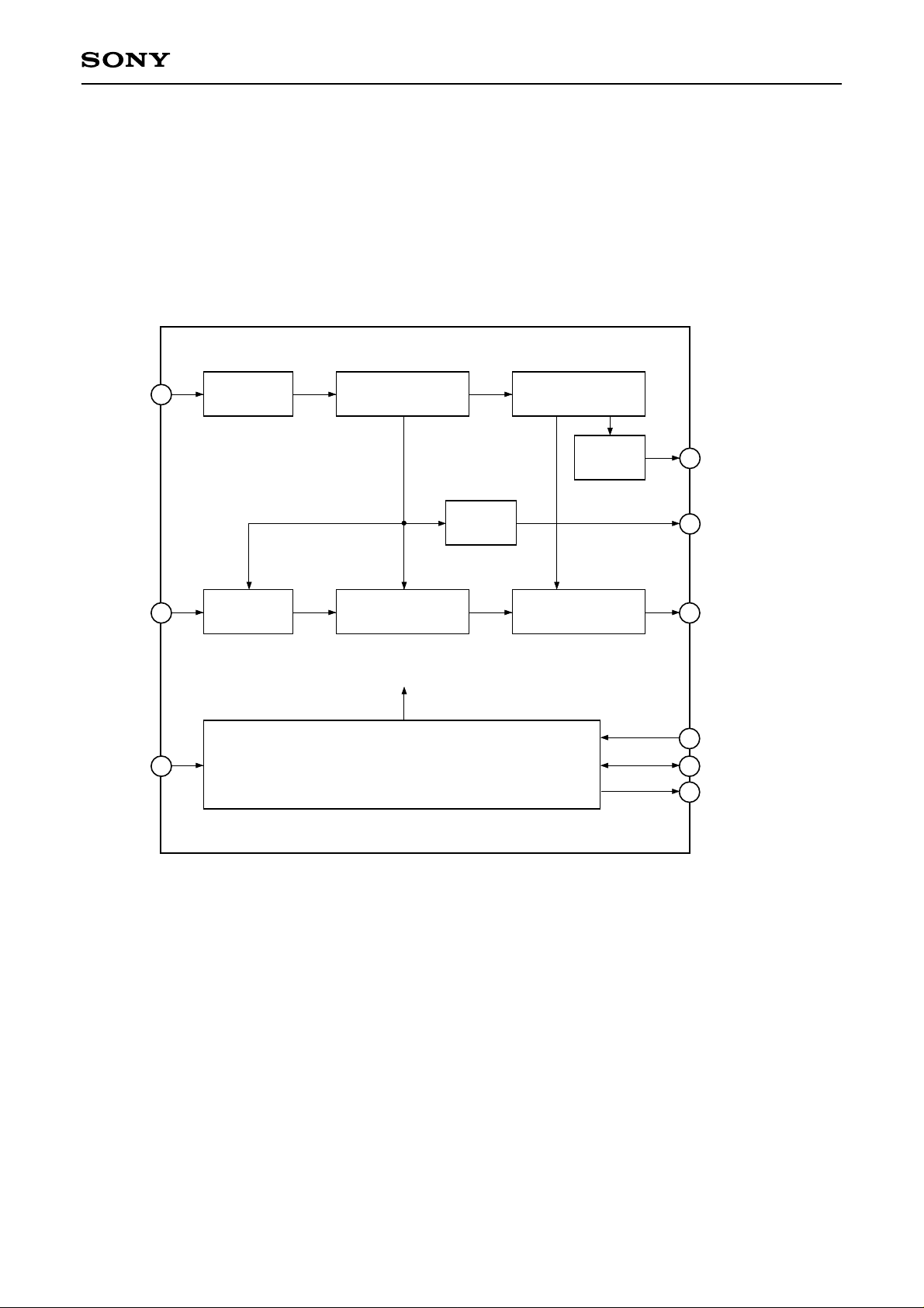
The CXD3511Q incorporates digital signal
processor type RGB driver, color shading correction,
selectable delay line and timing generator functions
onto a single IC. Operation is possible with a system
clock up to 200 [MHz] (max.). This IC can process
video signals in bands up to UXGA standard, and
can output the timing signals for driving various Sony
LCD panels such as SXGA and XGA.
CXD3511Q
240 pin QFP (Plastic)
Features
• Various picture quality adjustment functions such
as user adjustment, white balance adjustment and
gamma correction
• OSD MIX, black frame processing, mute and
limiter functions
• LCD panel color shading correction function
• Selectable delay line
• Drives various Sony data projector LCD panels
such as SXGA and XGA
• Controls the CXA3512R and CXA3562R sample-
and-hold drivers
• Line inversion and field inversion signal generation
• Supports AC drive of LCD panels during no signal
Applications
LCD projectors and other video equipment
Structure
Silicon gate CMOS IC
Absolute Maximum Ratings (VSS = 0V)
• Supply voltage VDD1 VSS – 0.5 to +3.0 V
VDD2 VSS – 0.5 to +4.0 V
• Input voltage VI VSS – 0.5 to VDD1 + 0.5 V
• Output voltage VO VSS – 0.5 to VDD1 + 0.5 V
• Storage temperature
Tstg –55 to +125 °C
• Junction temperature
Tj 125 °C
Recommended Operating Conditions
• Supply voltage VDD1 2.3 to 2.7 V
VDD2 3.0 to 3.6 V
• Operating temperature
Topr –20 to +75 °C
Sony reserves the right to change products and specifications without prior notice. This information does not convey any license by
any implication or otherwise under any patents or other right. Application circuits shown, if any, are typical examples illustrating the
operation of the devices. Sony cannot assume responsibility for any problems arising out of the use of these circuits.
– 1 –
E00Y06-PS
Page 2

Block Diagram
CXD3511Q
R, G, B IN
R, G, B OSD
YM
YS
PCTL
PCLK
PDAT
CLKC
CLKP
CLKN
CLKSEL1
CLKSEL2
PLLDIV
HDIN
VDIN
8 × 2 × 3
2 × 2 × 3
2
2
10
PARALLEL I/F
PLL
DQ
Q
DSD
10 × 2 × 3
TG
Direct Clear
R, G, B OUT
CLKOUT
CTRL
RGT, DWN
PCG, BLK, HST,
ENBR, ENBL, VSTR,
VSTL, VCKR, VCKL,
HCK1, DCK1, DCK2,
HCK2, DCK1X, DCK2X,
XRGT, FRP, XFRP,
PRG, DENB, CLP,
PO1, PO2, PO3, PO4,
PO5, PST, HD1, HD2
XCLR1
XCLR2
XCLR3
– 2 –
Page 3

Pin Configuration
CXD3511Q
R1IN2
R1IN1
R1IN0
R2IN7
R2IN6
V
R2IN5
R2IN4
R2IN3
R2IN2
R2IN1
R2IN0
G1IN7
G1IN6
G1IN5
V
G1IN4
G1IN3
G1IN2
G1IN1
G1IN0
G2IN7
G2IN6
G2IN5
G2IN4
G2IN3
V
G2IN2
G2IN1
G2IN0
B1IN7
B1IN6
B1IN5
B1IN4
B1IN3
B1IN2
B1IN1
V
B1IN0
B2IN7
B2IN6
B2IN5
B2IN4
B2IN3
B2IN2
B2IN1
B2IN0
R1OSD1
R1OSD0
V
G1OSD1
G1OSD0
B1OSD1
B1OSD0
YM1
R1IN5
R1IN6
R1IN7
VSSV
DD2
TEST6
TEST5
TEST4
TEST3
TEST2
TEST1
HD1
166167168169170171172173174175176177178179180
R1IN3
R1IN4
181
182
183
184
185
186
DD2
187
V
SS
188
189
190
191
192
193
194
195
196
197
DD1
198
SS
V
199
200
201
202
203
204
205
206
207
208
DD1
209
V
SS
210
211
212
213
214
215
216
217
218
219
220
DD1
221
V
SS
222
223
224
225
226
227
228
229
230
231
232
233
DD2
234
SS
V
235
236
237
238
239
240
DD1
PO5
CLP
PO4
VSSV
PRG
163
165
164
DENB
SHST
XFRP
DD1
FRP
V
HD2
PO1
PO2
PO3
PST
1 2 3 4 5 6 7 8 9 10 11 12 13 14 15 16 17 18 19 20 21 22 23 24 25 26 27 28 29 30 31 32 33 34 35 36 37 38 39 40
YS1
R2OSD1
R2OSD0
G2OSD1
G2OSD0
SS
DD2
V
YS2
YM2
V
B2OSD1
B2OSD0
PCTL
PCLK
PDAT9
SS
DD2
V
V
PDAT8
PDAT7
PDAT6
PDAT5
DD1
V
PDAT4
PDAT3
PDAT2
PDAT1
SS
V
PDAT0
XCLR1
XCLR2
XCLR3
VSSPCG
VDIN
HDIN
CTRL
SSVSS
V
DD1VDD2
DWN
VSTL
V
VCKL
DD1VDD1
V
CLKP
CLKC
DD2
ENBL
BLK
HST
VSSV
141142143144145146147148149150151152153154155156157158159160161162
41 42 43 44 53 54 55 56 57 58 59 60
SS
DD1
DD2
V
V
V
CLKN
CLKSEL1
SS
XRGT
RGT
HCK2
HCK1
V
DCK1
135136137138139140
DCK1X
134
133
132
131
45 46 47 48 49 50 51 52
SS
SS
V
V
PLLDIV
B2OUT0
B2OUT1
CLKOUT
CLKSEL2
130
SS
V
DCK2X
129
B2OUT2
B2OUT3
SS
DCK2
V
127128
DD2
V
B2OUT4
DD2
V
ENBR
126
125
SS
V
B2OUT5
124
VCKR
VSTR
123
B2OUT6
B2OUT7
122
R2OUT9
R1OUT8
121
B2OUT8
B2OUT9
120
119
118
117
116
115
114
113
112
111
110
109
108
107
106
105
104
103
102
101
100
99
98
97
96
95
94
93
92
91
90
89
88
87
86
85
84
83
82
81
80
79
78
77
76
75
74
73
72
71
70
69
68
67
66
65
64
63
62
61
R1OUT7
R1OUT6
R1OUT5
R1OUT4
R1OUT3
V
SS
DD2
V
R1OUT2
R1OUT1
R1OUT0
R2OUT9
R2OUT8
R2OUT7
R2OUT6
R2OUT5
R2OUT4
R2OUT3
R2OUT2
V
SS
V
DD1
V
DD2
R2OUT1
R2OUT0
G1OUT9
G1OUT8
G1OUT7
G1OUT6
G1OUT5
G1OUT4
G1OUT3
V
SS
V
DD1
G1OUT2
G1OUT1
G1OUT0
G2OUT9
V
DD2
G2OUT8
G2OUT7
G2OUT6
G2OUT5
G2OUT4
V
SS
V
DD1
G2OUT3
G2OUT2
G2OUT1
G2OUT0
B1OUT9
B1OUT8
B1OUT7
B1OUT6
B1OUT5
V
SS
DD2
V
B1OUT4
B1OUT3
B1OUT2
B1OUT1
B1OUT0
– 3 –
Page 4

Pin Description
Pin
No.
1
2
3
4
5
6
7
8
9
10
11
12
Symbol
YS1
R2OSD1
R2OSD0
G2OSD1
G2OSD0
VDD2
VSS
B2OSD1
B2OSD0
YM2
YS2
PCTL
I/O
I
OSD YS input (port 1)
I
OSD Red data input (port 2)
I
OSD Red data input (port 2)
I
OSD Green data input (port 2)
I
OSD Green data input (port 2)
—
I/O power supply
—
GND
I
OSD Blue data input (port 2)
I
OSD Blue data input (port 2)
I
OSD YM input (port 2)
I
OSD YS input (port 2)
I
Parallel I/F control signal input
Description
CXD3511Q
Input pin
processing for
open status
L
—
—
—
—
—
—
—
—
L
L
H
13
14
15
16
17
18
19
20
21
22
23
24
25
26
27
28
29
PCLK
PDAT9
PDAT8
PDAT7
PDAT6
VDD2
VSS
PDAT5
PDAT4
PDAT3
PDAT2
PDAT1
VDD1
PDAT0
XCLR1
XCLR2
XCLR3
I
Parallel I/F clock input
I
Parallel I/F data input
I
Parallel I/F data input
I
Parallel I/F data input
I
Parallel I/F data input
—
I/O power supply
—
GND
I
Parallel I/F data input
I
Parallel I/F data input
I
Parallel I/F data input
I
Parallel I/F data input
I
Parallel I/F data input
—
Internal operation power supply
I
Parallel I/F data input
I
External clear (Low: reset)
I
External clear (Low: reset)
I
External clear (Low: reset)
—
—
—
—
—
—
—
—
—
—
—
—
—
H
H
H
30
31
32
33
34
35
36
37
VSS
HDIN
VDIN
VSS
VSS
CLKC
VDD1
VDD1
—
GND
I
Horizontal sync signal input
I
Vertical sync signal input
—
GND
—
GND
I
Clock input (CMOS input)
—
Internal operation power supply
—
Internal operation power supply
—
—
—
—
—
—
—
—
– 4 –
Page 5

CXD3511Q
Pin
No.
38
39
40
41
42
43
44
45
46
47
48
49
50
51
52
Symbol
CLKP
CLKN
VDD2
CLKSEL1
VDD1
VSS
CLKSEL2
PLLDIV
VSS
CLKOUT
VSS
B2OUT0
B2OUT1
B2OUT2
B2OUT3
I/O
I
Clock input (small-amplitude differential input, positive polarity)
I
Clock input (small-amplitude differential input, negative polarity)
—
I/O power supply
I
Input clock selection. (High: CLKC, Low: CLKP, CLKN)
—
Internal operation power supply
—
GND
Internal clock path selection.
I
(High: no frequency division, Low: frequency division)
I
Internal PLL setting. (High: 55MHz or less, Low: 55MHz or more)
—
GND
O
Internal clock output (inverted output)
—
GND
O
Blue data output (port 2)
O
Blue data output (port 2)
O
Blue data output (port 2)
O
Blue data output (port 2)
Description
Input pin
processing for
open status
—
—
—
L
—
—
L
L
—
—
—
—
—
—
—
53
54
55
56
57
58
59
60
61
62
63
64
65
66
67
68
69
B2OUT4
VDD2
VSS
B2OUT5
B2OUT6
B2OUT7
B2OUT8
B2OUT9
B1OUT0
B1OUT1
B1OUT2
B1OUT3
B1OUT4
VDD2
VSS
B1OUT5
B1OUT6
O
Blue data output (port 2)
—
I/O power supply
—
GND
O
Blue data output (port 2)
O
Blue data output (port 2)
O
Blue data output (port 2)
O
Blue data output (port 2)
O
Blue data output (port 2)
O
Blue data output (port 1)
O
Blue data output (port 1)
O
Blue data output (port 1)
O
Blue data output (port 1)
O
Blue data output (port 1)
—
I/O power supply
—
GND
O
Blue data output (port 1)
O
Blue data output (port 1)
—
—
—
—
—
—
—
—
—
—
—
—
—
—
—
—
—
70
71
72
73
74
B1OUT7
B1OUT8
B1OUT9
G2OUT0
G2OUT1
O
Blue data output (port 1)
O
Blue data output (port 1)
O
Blue data output (port 1)
O
Green data output (port 2)
O
Green data output (port 2)
—
—
—
—
—
– 5 –
Page 6

CXD3511Q
Pin
No.
75
76
77
78
79
80
81
82
83
84
85
86
87
88
89
90
Symbol
G2OUT2
G2OUT3
VDD1
VSS
G2OUT4
G2OUT5
G2OUT6
G2OUT7
G2OUT8
VDD2
G2OUT9
G1OUT0
G1OUT1
G1OUT2
VDD1
VSS
I/O
O
Green data output (port 2)
O
Green data output (port 2)
—
Internal operation power supply
—
GND
O
Green data output (port 2)
O
Green data output (port 2)
O
Green data output (port 2)
O
Green data output (port 2)
O
Green data output (port 2)
—
I/O power supply
O
Green data output (port 2)
O
Green data output (port 1)
O
Green data output (port 1)
O
Green data output (port 1)
—
Internal operation power supply
—
GND
Description
Input pin
processing for
open status
—
—
—
—
—
—
—
—
—
—
—
—
—
—
—
—
91
92
93
94
95
96
97
98
99
100
101
102
103
104
105
106
107
G1OUT3
G1OUT4
G1OUT5
G1OUT6
G1OUT7
G1OUT8
G1OUT9
R2OUT0
R2OUT1
VDD2
VDD1
VSS
R2OUT2
R2OUT3
R2OUT4
R2OUT5
R2OUT6
O
Green data output (port 1)
O
Green data output (port 1)
O
Green data output (port 1)
O
Green data output (port 1)
O
Green data output (port 1)
O
Green data output (port 1)
O
Green data output (port 1)
O
Red data output (port 2)
O
Red data output (port 2)
—
I/O power supply
—
Internal operation power supply
—
GND
O
Red data output (port 2)
O
Red data output (port 2)
O
Red data output (port 2)
O
Red data output (port 2)
O
Red data output (port 2)
—
—
—
—
—
—
—
—
—
—
—
—
—
—
—
—
—
108
109
110
111
R2OUT7
R2OUT8
R2OUT9
R1OUT0
O
Red data output (port 2)
O
Red data output (port 2)
O
Red data output (port 2)
O
Red data output (port 1)
—
—
—
—
– 6 –
Page 7

CXD3511Q
Pin
No.
112
113
114
115
116
117
118
119
120
121
122
123
124
125
126
127
Symbol
R1OUT1
R1OUT2
VDD2
VSS
R1OUT3
R1OUT4
R1OUT5
R1OUT6
R1OUT7
R1OUT8
R1OUT9
VSTR
VCKR
ENBR
VDD2
VSS
I/O
O
Red data output (port 1)
O
Red data output (port 1)
—
I/O power supply
—
GND
O
Red data output (port 1)
O
Red data output (port 1)
O
Red data output (port 1)
O
Red data output (port 1)
O
Red data output (port 1)
O
Red data output (port 1)
O
Red data output (port 1)
O
Vertical display start timing pulse output
O
Vertical display transfer clock output
O
Gate enable pulse output
—
I/O power supply
—
GND
Description
Input pin
processing for
open status
—
—
—
—
—
—
—
—
—
—
—
—
—
—
—
—
128
129
130
131
132
133
134
135
136
137
138
139
140
141
142
143
144
DCK2
DCK2X
VSS
DCK1X
DCK1
VSS
HCK1
HCK2
RGT
XRGT
VDD2
VSS
HST
BLK
ENBL
VCKL
VDD2
O
DCK2 pulse output
O
DCK2X pulse output
—
GND
O
DCK1X pulse output
O
DCK1 pulse output
—
GND
O
Horizontal display transfer clock output 1
O
Horizontal display transfer clock output 2
I/O
Horizontal scan direction switching signal I/O
Horizontal scan direction switching signal output (reversed
O
polarity of RGT)
—
I/O power supply
—
GND
O
Horizontal display start timing pulse output
O
BLK pulse output
O
Gate enable pulse output
O
Vertical display transfer clock output
—
I/O power supply
—
—
—
—
—
—
—
—
—
—
—
—
—
—
—
—
—
145
146
147
VDD1
VSTL
DWN
—
Internal operation power supply
O
Vertical display start timing pulse output
I/O
Vertical scan direction switching signal I/O
– 7 –
—
—
—
Page 8

CXD3511Q
Pin
No.
148
149
150
151
152
153
154
155
156
157
158
159
160
161
162
Symbol
CTRL
PCG
VSS
PST
PO3
PO2
PO1
HD2
VDD1
FRP
XFRP
SHST
DENB
PRG
VDD1
I/O
Scan direction control method switching
I
(Low: internal register, High: external)
O
Collective precharge timing pulse output
—
GND
O
Dot sequential precharge start timing pulse output
O
Parallel output 3
O
Parallel output 2
O
Parallel output 1
O
Horizontal auxiliary pulse output 2
—
Internal operation power supply
O
AC drive inversion timing pulse output
O
AC drive inversion timing pulse output (reversed polarity of FRP)
O
SHST pulse output
O
DENB pulse output
O
2-step precharge timing pulse output
—
Internal operation power supply
Description
Input pin
processing for
open status
L
—
—
—
—
—
—
—
—
—
—
—
—
—
—
163
164
165
166
167
168
169
170
171
172
173
174
175
176
177
178
179
VSS
PO4
CLP
PO5
HD1
TEST1
TEST2
TEST3
TEST4
TEST5
TEST6
VDD2
VSS
R1IN7
R1IN6
R1IN5
R1IN4
—
GND
O
Parallel output 4
O
CLP pulse output
O
Parallel output 5
O
Horizontal auxiliary pulse output 1
—
Test pin (Connect to GND.)
—
Test pin (Connect to GND.)
—
Test pin (Connect to VDD2.)
—
Test pin (Connect to VDD2.)
—
Test pin (Connect to VDD2.)
—
Test pin (Connect to VDD2.)
—
I/O power supply
—
GND
I
Red data input (port 1)
I
Red data input (port 1)
I
Red data input (port 1)
I
Red data input (port 1)
—
—
—
—
—
—
—
—
—
—
—
—
—
—
—
—
—
180
181
182
183
184
R1IN3
R1IN2
R1IN1
R1IN0
R2IN7
I
Red data input (port 1)
I
Red data input (port 1)
I
Red data input (port 1)
I
Red data input (port 1)
I
Red data input (port 2)
—
—
—
—
—
– 8 –
Page 9

CXD3511Q
Pin
No.
185
186
187
188
189
190
191
192
193
194
195
196
197
198
199
200
Symbol
R2IN6
VDD2
VSS
R2IN5
R2IN4
R2IN3
R2IN2
R2IN1
R2IN0
G1IN7
G1IN6
G1IN5
VDD1
VSS
G1IN4
G1IN3
I/O
I
Red data input (port 2)
—
I/O power supply
—
GND
I
Red data input (port 2)
I
Red data input (port 2)
I
Red data input (port 2)
I
Red data input (port 2)
I
Red data input (port 2)
I
Red data input (port 2)
I
Green data input (port 1)
I
Green data input (port 1)
I
Green data input (port 1)
—
Internal operation power supply
—
GND
I
Green data input (port 1)
I
Green data input (port 1)
Description
Input pin
processing for
open status
—
—
—
—
—
—
—
—
—
—
—
—
—
—
—
—
201
202
203
204
205
206
207
208
209
210
211
212
213
214
215
216
217
G1IN2
G1IN1
G1IN0
G2IN7
G2IN6
G2IN5
G2IN4
G2IN3
VDD1
VSS
G2IN2
G2IN1
G2IN0
B1IN7
B1IN6
B1IN5
B1IN4
I
Green data input (port 1)
I
Green data input (port 1)
I
Green data input (port 1)
I
Green data input (port 2)
I
Green data input (port 2)
I
Green data input (port 2)
I
Green data input (port 2)
I
Green data input (port 2)
—
Internal operation power supply
—
GND
I
Green data input (port 2)
I
Green data input (port 2)
I
Green data input (port 2)
I
Blue data input (port 1)
I
Blue data input (port 1)
I
Blue data input (port 1)
I
Blue data input (port 1)
—
—
—
—
—
—
—
—
—
—
—
—
—
—
—
—
—
218
219
220
221
B1IN3
B1IN2
B1IN1
VDD1
I
Blue data input (port 1)
I
Blue data input (port 1)
I
Blue data input (port 1)
—
Internal operation power supply
—
—
—
—
– 9 –
Page 10

CXD3511Q
Pin
No.
222
223
224
225
226
227
228
229
230
231
232
233
234
235
236
237
Symbol
SS
V
B1IN0
B2IN7
B2IN6
B2IN5
B2IN4
B2IN3
B2IN2
B2IN1
B2IN0
R1OSD1
R1OSD0
VDD2
VSS
G1OSD1
G1OSD0
I/O
—
GND
I
Blue data input (port 1)
I
Blue data input (port 2)
I
Blue data input (port 2)
I
Blue data input (port 2)
I
Blue data input (port 2)
I
Blue data input (port 2)
I
Blue data input (port 2)
I
Blue data input (port 2)
I
Blue data input (port 2)
I
OSD red data input (port 1)
I
OSD red data input (port 1)
—
I/O power supply
—
GND
I
OSD green data input (port 1)
I
OSD green data input (port 1)
Description
Input pin
processing for
open status
—
—
—
—
—
—
—
—
—
—
—
—
—
—
—
—
238
B1OSD1
239
B1OSD0
240
YM1
∗
H: Pull-up, L: Pull-down
I
OSD blue data input (port 1)
I
OSD blue data input (port 1)
I
OSD YM input (port 1)
—
—
L
– 10 –
Page 11

CXD3511Q
Electrical Characteristics
DC Characteristics (Topr = –20 to +75°C, VSS = 0V)
Item Symbol Applicable pins Conditions Min. Typ. Max.
Supply
voltage
Input
voltage 1
Input
voltage 2
Input
voltage 3
VDD1
VDD2
VIH1
VIL1
VIH2
VIL2
VC
VIH3
1
∗
HDIN, VDIN, PCTL,
PCLK, PDAT0 to PDAT9
2
∗
CLKP, CLKN
VIL3
Output
voltage
Current
consumption
1
∗
Input pins other than those indicated in items Input voltage 2 and Input voltage 3.
2
∗
VIH3 > VC (max.) and VIL3 < VC (min.).
3
∗
Tj [°C] ≥ Toprmax [°C] + θja [°C/W] × PD [W].
VOH
VOL
PD
All output pins
3
∗
—
—
—
—
CMOS input cell
CMOS Schmitt
trigger input cell
Small-amplitude
differential input
—
—
CLKP = 200MHz
2.3
3.0
2.0
–0.3
0.8VDD2
–0.3
1.718
1.868
VSS
VDD2 – 0.5
VSS
—
2.5
3.3
—
—
—
—
2.0
VC + 0.4
VC – 0.4
—
—
2600
(Tj = 125 [°C], Toprmax = 75 [°C], θja = 16 [°C/W], when mounted on a 4-layer substrate)
2.7
3.6
DD2 + 0.3
V
0.8
V
DD2 + 0.3
0.2VDD2
2.281
VDD2
2.131
VDD2
0.2
3120
Unit
V
mW
AC Characteristics (Topr = –20 to +75°C, VDD1 = 2.5 ± 0.2V, VDD2 = 3.3 ± 0.3V, VSS = 0V)
Item Symbol Applicable pins Conditions Min. Typ. Max. Unit
Clock input period
Input setup time
tis
—
CLKP, CLKN, CLKC
RGB input, OSD input,
—
—
5
2.5
—
—
—
—
HDIN, VDIN
Input hold time
Output rise/fall
delay time
Output rise/fall
delay time
Output rise/fall
delay time
Cross-point time
difference
HCK1 duty
tih
tor/tof
tor/tof
tor/tof
∆t
th/(th + tl)
4
∗
RGB output
CLKOUT
HCK1, HCK2, DCK1,
DCK1X, DCK2, DCK2X
HCK1
—
CL = 20pF
CL = 20pF
CL = 50pF
CL = 20pF
CL = 20pF
1.5
2
2
1.5
–5
48
—
5
4
4.5
—
50
—
10
ns
8
8.5
5
52
%
HCK2 duty
tl/(th + tl)
Phase compensation
PLL operating
—
frequency
4
∗
Output pins other than RGB output, CLKOUT, PO1 to PO5, RGT, XRGT and DWN.
HCK2
—
CL = 20pF
PLLDIV = L
PLLDIV = H
48
55
27.5
50
—
—
52
100
MHz
55
– 11 –
Page 12

Timing Definition
1/2 frequencydivided inputs
RGB input, OSD input,
HDIN, VDIN
1/2 frequencydivided inputs
Outputs other than CLKOUT
Outputs other than CLKOUT
CLKP, CLKC
CLKN
CLKP, CLKC
CLKN
CLKP, CLKC
CLKN
CLKP, CLKC
CLKN
CLKOUT
VC, 50%
VC
VC, 50%
VC
tof
tor
tis tih
VC, 50%
VC
VC, 50%
VC
50% 50%
tor
50%
50%
VC, 50%
VC
VC, 50%
50%
IH3
V
V
IL3
V
IH3
V
IL3
V
IH3
V
IL3
V
IH3
V
IL3
V
DD2
V
SS
IH3
V
V
IL3
V
IH3
V
IL3
V
IH3
V
IL3
V
IH3
V
IL3
V
DD2
V
SS
V
DD2
V
SS
V
DD2
V
SS
CXD3511Q
, V
DD2
, V
SS
, V
DD2
, V
SS
, V
DD2
, V
SS
, V
DD2
, V
SS
HCK1, DCK1, DCK2
HCK2, DCK1X, DCK2X
CHK1, HCK2
tof
50%
50%
50%
50%
∆t∆t
50% 50% 50%
th tl
– 12 –
V
DD2
V
SS
V
DD2
V
SS
V
DD2
V
SS
Page 13

CXD3511Q
Parallel I/F Block AC Characteristics (Topr = –20 to +75°C, VDD1 = 2.5 ± 0.2V, VDD2 = 3.3 ± 0.3V, VSS = 0V)
Item
PCTL setup time with respect to rise of PCLK
PCTL hold time with respect to rise of PCLK
PDAT[9:0] setup time with respect to rise of PCLK
PDAT[9:0] hold time with respect to rise of PCLK
PCLK pulse width
5
∗
T: Master clock (CLKP, CLKN, CLKC) period [ns]
Timing Definition
tcs
50%PCTL
tw tw
PCLK
PDAT[9:0]
50% 50%
tds tdh
50% 50%
Symbol
tcs
tch
tds
tdh
tw
tch
8T
50%
Min.
∗
8T
4T
4T
4T
Typ.
5
—
—
—
—
—
DD2
V
V
SS
V
DD2
V
SS
V
DD2
V
SS
Max.
—
—
—
—
—
Power-on and Initialization of Internal Circuit
As for this IC, two systems of supply voltage should be turned on simultaneously. The initialization of the
internal circuit should be also performed by maintaining the system clear pin at low during the specified time
after setting the supply voltage in the range of recommended operating conditions and stabilizing as shown in
the figure below. Keep in mind that the internal circuit may not be initialized correctly if system clear
cancellation is performed before the supply voltage is set in the range of the recommended operating
conditions.
V
DD1
, V
DD2
V
DD1
, V
DD2
XCLR1, XCLR2,
XCLR3
TR
TR > 200ns
V
SS
V
DD2
V
SS
– 13 –
Page 14

CXD3511Q
Description of Operation
1. Description of Input Pins
(a) System clear pins (XCLR1, XCLR2 and XCLR3)
All internal circuits are initialized by setting XCLR1 (Pin 27) low. In addition, the internal PLL is initialized by
setting XCLR2 (Pin 28) low, and RGB output is initialized (preset) by setting XCLR3 (Pin 29) low.
Initialization should be performed when power is turned on. There are no particular restrictions on the
initialization order.
(b) Sync signal input pins (HDIN and VDIN)
Horizontal and vertical separate sync signals are input to HDIN (Pin 31) and VDIN (Pin 32), respectively. The
CXD3511Q supports only non-inter lace sync signals with a dot clock of 200MHz or less.
(c) Master clock input pins (CLKP/CLKN and CLKC)
Phase comparison is performed by an external circuit and a clock synchronized to the sync signal is input. The
master clock input pins have two systems consisting of CLKP/CLKN (Pins 38 and 39) for small-amplitude
differential input (center level: 2.0V, amplitude: ±0.4V), and CLKC (Pin 35) for CMOS level input. In addition, be
sure to make the number of dot clocks in 1H as even number.
Note that if there is an odd number of dot clocks, the internal phase compensation PLL will not operate
properly.
(d) Clock selection pins (CLKSEL1 and CLKSEL2)
The master clock input pins can input either the system dot clock or the 1/2 frequency-divided clock. The
internal clock path is selected according to CLKSEL1 (Pin 41) and CLKSEL2 (Pin 44).
Setting
Symbol
CLKSEL1
CLKSEL2
Input clock selection
Clock input pin selection
Function
L
CLKP/CLKN input
Dot clock input
H
CLKC input
1/2 frequency-divided clock input
(e) PLL setting pin (PLLDIV)
PLLDIV (Pin 45) sets the divider setting of the internal phase compensation PLL circuit. Set PLLDIV low when
the internal clock frequency is 55 to 100MHz, or high when 27.5 to 55MHz. In addition, note that the frequency
of the clock input to the CXD3511Q must be within the phase compensation PLL operating range, even during
free running.
– 14 –
Page 15

CXD3511Q
(f) RGB signal input pins (R1IN, R2IN, G1IN, G2IN, B1IN and B2IN)
These pins input RGB signals that have been demultiplexed to 1:2. The Red signal is input to R1IN (Pins 176
to 183) and R2IN (Pins 184, 185 and 188 to 193), the Green signal to G1IN (Pins 194 to 196 and 199 to 203)
and G2IN (Pins 204 to 208 and 211 to 213), and the Blue signal to B1IN (Pins 214 to 220 and 223) and B2IN
(Pins 224 to 231).
(g) OSD signal input pins (R1OSD, R2OSD, G1OSD, G2OSD, B1OSD, B2OSD, YM1, YM2, YS1 and YS2)
These pins input OSD signals that have been demultiplexed to 1:2. The Red signal is input to R1OSD (Pins
232 and 233) and R2OSD (Pins 2 and 3), the Green signal to G1OSD (Pins 236 and 237) and G2OSD (Pins
4 and 5), and the Blue signal to B1OSD (Pins 238 and 239) and B2OSD (Pins 8 and 9). In addition, the YM
signal is input to YM1 (Pin 240) and YM2 (Pin 10), and the YS signal to YS1 (Pin 1) and YS2 (Pin 11).
– 15 –
Page 16

CXD3511Q
2. RGB Signal and OSD Signal Pipeline Delay
The RGB signal I/O pipeline delay is 54 dot clocks. In addition, the OSD, YM and YS signal pipeline delay is 34
dot clocks. Note that the phase relationship between each clock and the RGB signals is as shown in the
figures below. This relationship is the same for the OSD, YM and YS signals.
(1) CLKPOL = L
HDIN input (negative polarity)
Dot clock
1/2 frequency-divided clock
R1, G1, B1OUT
R2, G2, B2OUT
(2) CLKPOL = H
HDIN input (negative polarity)
1/2 frequency-divided clock
R1, G1, B1IN
R2, G2, B2IN
CLKOUT
Dot clock
R1, G1, B1IN
R2, G2, B2IN
N – 2
N – 1 N + 1 N + 3 N + 5 N + 7 N + 9 N + 11 N + 13 N + 15 N + 17 N + 19
N – 56 N – 54 N – 52 N – 50 N – 48 N – 46 N – 44 N – 42 N – 40 N – 38 N – 36
N – 55 N – 53 N – 51 N – 49 N – 47 N – 45 N – 43 N – 41 N – 39 N – 37 N – 35
N – 2 N N + 2 N + 4 N + 6 N + 8 N + 10 N + 12 N + 14 N + 16 N + 18
N – 1 N + 1 N + 3 N + 5 N + 7 N + 9 N + 11 N + 13 N + 15 N + 17 N + 19
N N + 2 N + 4 N + 6 N + 8 N + 10 N + 12 N + 14 N + 16 N + 18
CLKOUT
R1, G1, B1OUT
R2, G2, B2OUT
N – 56 N – 54 N – 52 N – 50 N – 48 N – 46 N – 44 N – 42 N – 40 N – 38 N – 36
N – 55 N – 53 N – 51 N – 49 N – 47 N – 45 N – 43 N – 41 N – 39 N – 37 N – 35
– 16 –
Page 17

3. Description of DSD Block Signal Processing Functions
The DSD block signal processing flow is shown below.
CXD3511Q
R, G, B IN
Sub bright Mute 1 OSD
Selectable
delay line
Data path
switch
Black
frame
Mute 2 Limiter Post bright
Pre gain Pre bright User gain User bright Sub gain
YS, YM, R, G, B OSD
Pattern
generator
Post gain
Gamma
correction
Cycle
offset
Color shading
correction
R, G, B OUT
The various signal processing functions are described below. Note that the coefficients used for each
arithmetic operation are set through the parallel I/F block. See the individual descriptions of each parallel I/F
block item for a detailed description of the parallel I/F block.
(a) Data path switch block
This block can switch the path of the data input to ports 1 and 2. The setting is as follows.
Select signal: 1 = Path switched, 0 = Path not switched (Set independently for R, G and B)
Select signal (R, G, B_DAT_SW)
Input (port 1)
Input (port 2)
8
8
Selector
Selector
8
8
Output (port 1)
Output (port 2)
– 17 –
Page 18

CXD3511Q
(b) Pre gain block
This block performs multiplication processing independently for ports 1 and 2. The settings are as follows.
Coefficient: 8 bits
Gain setting: 0 to 1.9921875 (= 255/128) times, variable in 256 steps
(Set independently for R, G and B ports 1 and 2)
Multiplication is performed using the 8-bit input and an 8-bit coefficient, and the upper 10 bits c[15:6] of the
operation results are output. Next, the c[6] value is checked and rounding is performed to 9 bits. The MSB of
the rounded 9 bits is checked, clipping is performed, and the lower 8 bits are output.
Coefficient
b[7:0]
Input
a[7:0]
8
a × b
108
c[15:6]
Rounding
and
clipping
8
Output
(c) Pre bright block
This block performs addition and subtraction processing independently for ports 1 and 2. The settings are as
follows.
Coefficient: 5 bits with code, MSB = code bit
Bright setting: –16 to +15 scales, variable with an accuracy of 1 bit
(Set independently for R, G and B ports 1 and 2)
Multiplication is performed using the 8-bit input and a 5-bit coefficient with code. The coefficient MSB is the
code bit. Addition is performed when b[4] = 0, and subtraction when b[4] = 1. However, when performing
subtraction, set the two's complement in the lower bits of the coefficient. When the operation results overflow
or underflow, clipping is performed.
Input
a[7:0]
Coefficient
b[4:0]
8
5
Addition/subtraction
and
clipping
8
Output
(d) User gain block
This block performs multiplication processing independently for ports 1 and 2. The settings are as follows.
Coefficient: 8 bits
Gain setting: 0 to 7.96875 (= 255/32) times, variable in 256 steps
(Settings shared by R, G and B)
Multiplication is performed using the 8-bit input and an 8-bit coefficient, and the upper 12 bits c[15:4] of the
operation results are output. Next, the c[4] value is checked and rounding is performed to 11 bits. The MSB of
the rounded 11 bits is checked, clipping is performed, and the lower 10 bits are output.
Coefficient
b[7:0]
Input
a[7:0]
8
a × b
128
c[15:4]
Rounding
and
clipping
10
Output
– 18 –
Page 19

CXD3511Q
(e) User bright block
This block performs addition and subtraction processing as the user control bright adjustment. The settings are
as follows.
Coefficient: 11 bits with code, MSB = code bit
Bright setting: –1024 to +1023 scales, variable with an accuracy of 1 bit
(Settings shared by R, G and B)
Multiplication is performed using the 10-bit input and an 11-bit coefficient with code. The coefficient MSB is the
code bit. Addition is performed when b[10] = 0, and subtraction when b[10] = 1. However, when performing
subtraction, set the two's complement in the lower bits of the coefficient. When the operation results overflow
or underflow, clipping is performed.
Input
a[9:0]
Coefficient
b[10:0]
10
11
Addition/subtraction
and
clipping
10
Output
(f) Sub gain block
This block performs multiplication processing as the white balance gain adjustment. The settings are as follows.
Coefficient: 8 bits
Gain setting: 0 to 3.984375 (255/64) times, variable in 256 steps
(Set independently for R, G and B)
Multiplication is performed using the 10-bit input and an 8-bit coefficient, and the upper 13 bits c[17:5] of the
operation results are output. Next, the c[5] value is checked and rounding is performed to 12 bits. The upper 2
bits of the rounded 12 bits is checked, clipping is performed, and the lower 10 bits are output.
Coefficient
b[7:0]
Input
a[9:0]
8
a × b
1310
c[17:5]
Rounding
and
clipping
10
Output
(g) Sub bright block
This block performs addition and subtraction processing as the white balance bright adjustment. The settings
are as follows.
Coefficient: 11 bits with code, MSB = code bit
Bright setting: –1024 to +1023 scales, variable with an accuracy of 1 bit
(Set independently for R, G and B)
Multiplication is performed using the 10-bit input and an 11-bit coefficient with code. The coefficient MSB is the
code bit. Addition is performed when b[10] = 0, and subtraction when b[10] = 1. However, when performing
subtraction, set the two's complement in the lower bits of the coefficient. When the operation results overflow
or underflow, clipping is performed.
Input
a[9:0]
Coefficient
b[10:0]
10
11
Addition/subtraction
and
clipping
10
Output
– 19 –
Page 20

CXD3511Q
(h) Black frame block
This block performs processing to fix the blanking period of the video signal to the desired level regardless of
the front-end signal processing results.
If the number of pixels calculated from the effective period of the video signal to be displayed is less than the
number of pixels of the LCD panel on which the signal is to be displayed, the blanking period of the video
signal is displayed in the excess pixels. At this time, the displayed blanking period can be fixed to the desired
level regardless of the gain and bright adjustment or other picture quality adjustment results by processing with
this block. The settings are as follows.
FRM_ON: 1 = Black frame processing ON, 0 = OFF
FRM_DAT: Black frame level setting
FRM_H1, FRM_H2: Set the black frame horizontal display range in 1-dot units
FRM_V1, FRM_V2: Set the black frame vertical display range in 1-line units
(All settings shared by R, G and B)
Here, the desired range of the video signal is replaced with 10-bit data (FRM_DAT) by switching the video
signal (port 1 and por t 2) and the coefficients using the pulse output from the pulse decoder.
Internal HD
Internal VD
Internal MCLK
Processing ON/OFF
(FRM_ON)
Input (port 1)
Coefficient (FRM_DAT)
Input (port 2)
Pulse decoder
10
10
10
12
12
11
11
Selector
Selector
Horizontal display range (FRM_H1)
Horizontal display range (FRM_H2)
Vertical display range (FRM_V1)
Vertical display range (FRM_V2)
Output (port 1)
10
Output (port 2)
10
(i) Mute 1 block
This block performs mute processing by replacing the video signal with data of the desired level. The settings
are as follows.
MUTE1_ON: 1 = Mute processing ON, 0 = OFF (Setting shared by R, G and B)
R, G, B_MUTE1: RGB mute data (Set independently for R, G and B)
Input
Coefficient
(R, G, B_MUTE1)
Select signal (MUTE1_ON)
10
10
Selector
– 20 –
10
Output
Page 21

CXD3511Q
(j) Pattern generator block
This block generates and outputs the set fixed pattern independently of the input signal. This function is valid
when PG_ON = 1. When PG_R (G, B)_ON is "0", the signal level goes to 000h respectively for R, G and B.
The raster display pattern is displayed in the effective area, and all other display patterns are displayed in the
window area. Here, the effective area is set by PG_HST, PG_HSTP, PG_VST and PG_VSTP, and the window
area is set by PG_HWST, PG_HWSTP, PG_VWST and PG_VWSTP.
The display pattern signal level is set independently for R, G and B by PG_SIG1R (G, B)[9:0] and PG_SIG2R
(G, B)[9:0]. Within the effective area, the pattern and non-pattern signal levels can be switched by PG_R (G,
B)_SEL. At this time, the signal level outside the effective area goes to 000h. During horizontal ramp, horizontal
stair, vertical ramp and vertical stair display, the PG_SIG1R (G, B)[9:0] and PG_SIG2R (G, B)[9:0] settings are
invalid.
The display patterns and signal levels are as follows.
(1) Raster display
When PG_PAT[2:0] = 0h, a raster is displayed.
PG_SIG2R (G, B)
PG_R (G, B)_SEL
PG_PAT[2:0]
PG_STRP_SW
PG_STAIR_SW
PG_R (G, B)_SEL
PG_PAT[2:0]
0
0h
x
x
1
0h
PG_SIG1R (G, B)
– 21 –
PG_STRP_SW
PG_STAIR_SW
x
x
x: Don't care
Page 22

(2) Window display
When PG_PAT[2:0] = 1h, a window is displayed.
CXD3511Q
PG_SIG2R (G, B)
PG_SIG1R (G, B)
PG_SIG1R (G, B)
PG_SIG2R (G, B)
PG_R (G, B)_SEL
PG_PAT[2:0]
PG_STRP_SW
PG_STAIR_SW
PG_R (G, B)_SEL
PG_PAT[2:0]
PG_STRP_SW
PG_STAIR_SW
0
1h
x
x
1
1h
x
x
– 22 –
x: Don't care
Page 23

CXD3511Q
(3) Vertical stripe display
When PG_PAT[2:0] = 2h and PG_STRP_SW = 0, vertical stripes are displayed.
The stripe period is set by PG_STEP in 2-dot units. The stripe width is set by PG_WIDTH in 1-dot units.
PG_SIG2R (G, B)
PG_SIG1R (G, B)
PG_SIG1R (G, B)
PG_R (G, B)_SEL
PG_PAT[2:0]
PG_STRP_SW
PG_STAIR_SW
PG_R (G, B)_SEL
PG_PAT[2:0]
PG_STRP_SW
PG_STAIR_SW
0
2h
0
x
1
2h
0
x
PG_SIG2R (G, B)
x: Don't care
– 23 –
Page 24

CXD3511Q
(4) Diagonal stripes
When PG_PAT[2:0] = 2h and PG_STRP_SW = 1, diagonal stripes are displayed.
The stripe period is set by PG_STEP in 2-dot units. The stripe width is set by PG_WIDTH in 1-dot units.
PG_SIG2R (G, B)
PG_SIG1R (G, B)
PG_SIG1R (G, B)
PG_R (G, B)_SEL
PG_PAT[2:0]
PG_STRP_SW
PG_STAIR_SW
PG_R (G, B)_SEL
PG_PAT[2:0]
PG_STRP_SW
PG_STAIR_SW
0
2h
1
x
1
2h
1
x
PG_SIG2R (G, B)
x: Don't care
– 24 –
Page 25
CXD3511Q
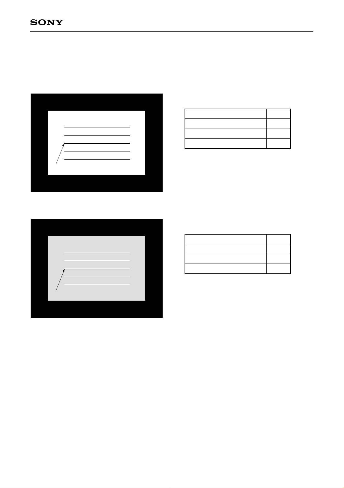
(5) Horizontal stripes
When PG_PAT[2:0] = 3h, horizontal stripes are displayed.
The stripe period is set by PG_STEP in 2-dot units. The stripe width is set by PG_WIDTH in 1-dot units.
PG_SIG2R (G, B)
PG_SIG1R (G, B)
PG_SIG1R (G, B)
PG_R (G, B)_SEL
PG_PAT[2:0]
PG_STRP_SW
PG_STAIR_SW
PG_R (G, B)_SEL
PG_PAT[2:0]
PG_STRP_SW
PG_STAIR_SW
0
3h
x
x
1
3h
x
x
PG_SIG2R (G, B)
x: Don't care
– 25 –
Page 26
CXD3511Q
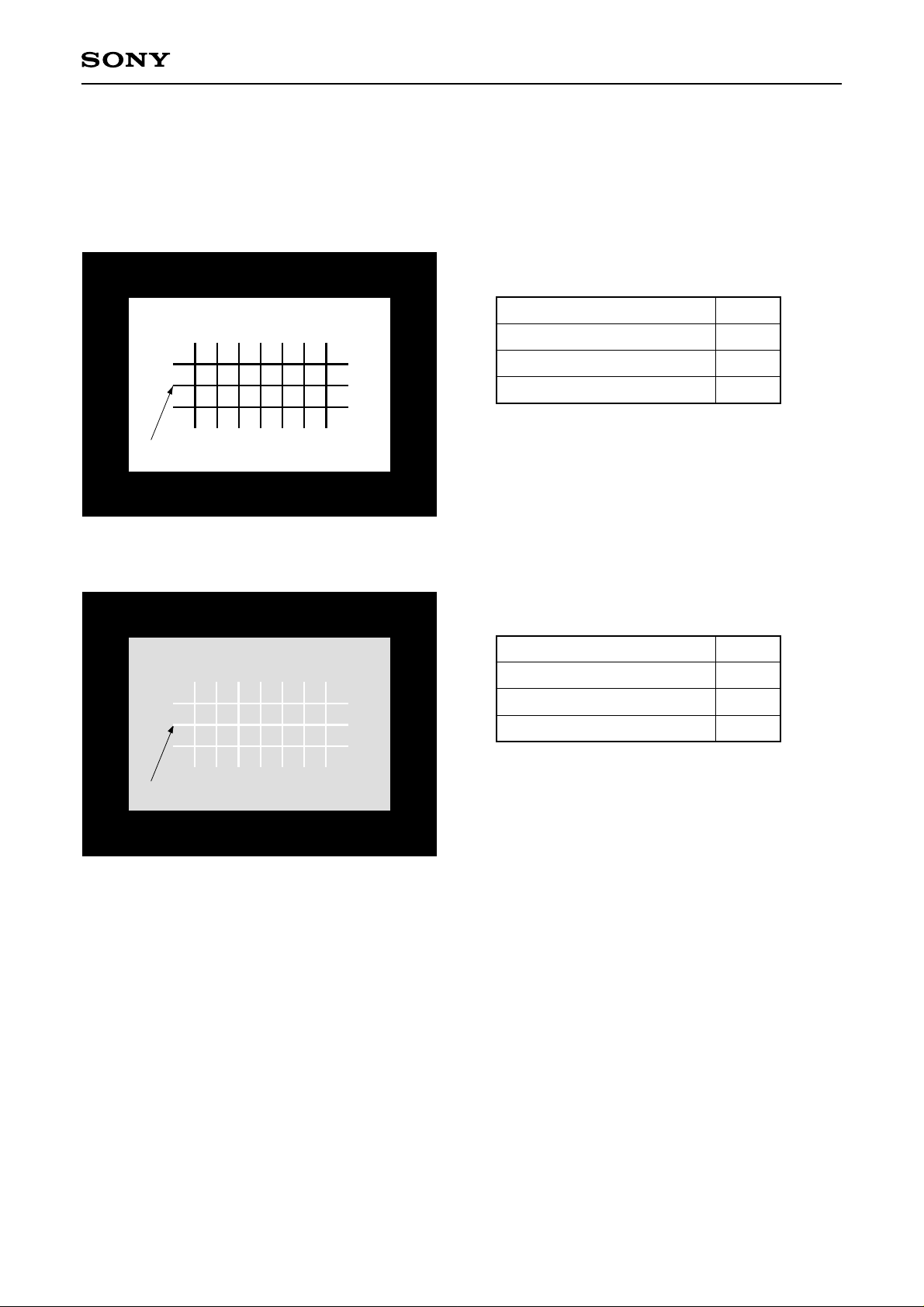
(6) Cross hatch
When PG_PAT[2:0] = 4h, a cross hatch is displayed.
The stripe period is set by PG_STEP in 2-dot units. The stripe width is set by PG_WIDTH in 1-dot units.
PG_SIG2R (G, B)
PG_SIG1R (G, B)
PG_SIG1R (G, B)
PG_R (G, B)_SEL
PG_PAT[2:0]
PG_STRP_SW
PG_STAIR_SW
PG_R (G, B)_SEL
PG_PAT[2:0]
PG_STRP_SW
PG_STAIR_SW
0
4h
x
x
1
4h
x
x
PG_SIG2R (G, B)
x: Don't care
– 26 –
Page 27
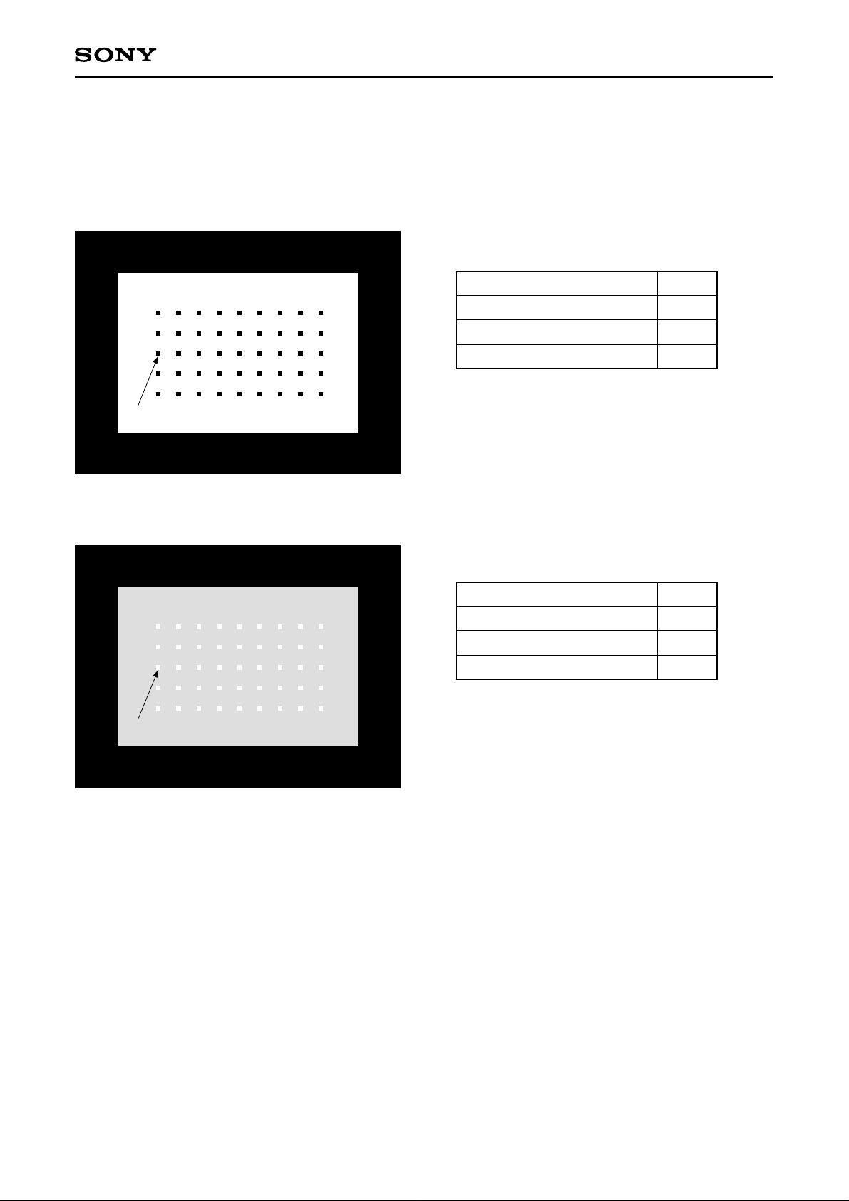
(7) Dots
When PG_PAT[2:0] = 5h, a dot pattern is displayed.
The dot period is set by PG_STEP in 2-dot units. The dot width is set by PG_WIDTH in 1-dot units.
CXD3511Q
PG_SIG2R (G, B)
PG_SIG1R (G, B)
PG_SIG1R (G, B)
PG_R (G, B)_SEL
PG_PAT[2:0]
PG_STRP_SW
PG_STAIR_SW
PG_R (G, B)_SEL
PG_PAT[2:0]
PG_STRP_SW
PG_STAIR_SW
0
5h
x
x
1
5h
x
x
PG_SIG2R (G, B)
x: Don't care
– 27 –
Page 28
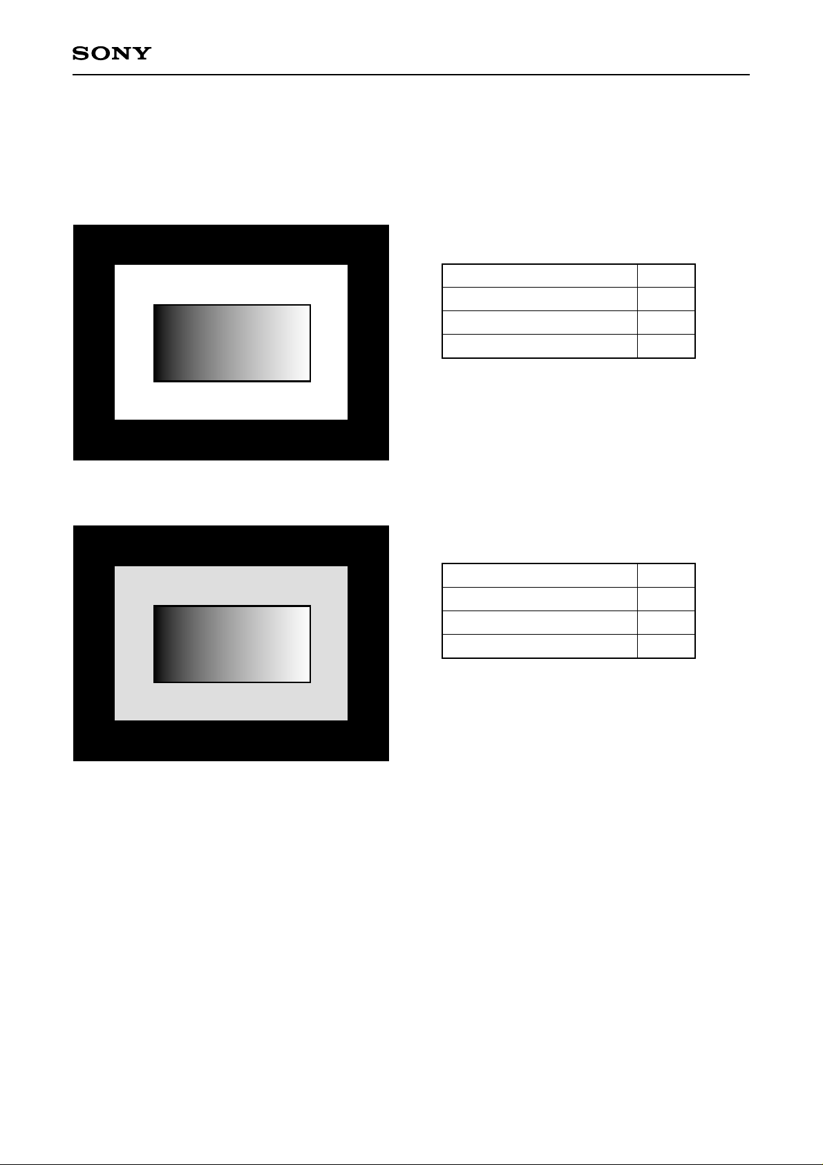
(8) Horizontal ramp
When PG_PAT[2:0] = 6h and PG_STAIR_SW = 0, a horizontal ramp is displayed.
The signal level is incremented from 000h by one bit for each dot.
CXD3511Q
PG_SIG2R (G, B)
PG_SIG1R (G, B)
PG_R (G, B)_SEL
PG_PAT[2:0]
PG_STRP_SW
PG_STAIR_SW
PG_R (G, B)_SEL
PG_PAT[2:0]
PG_STRP_SW
PG_STAIR_SW
0
6h
x
0
1
6h
x
0
– 28 –
x: Don't care
Page 29

(9) Horizontal stair
When PG_PAT[2:0] = 6h and PG_STAIR_SW = 1, a horizontal stair is displayed.
The signal level is incremented from 000h by 64 bits for each 64 dots.
CXD3511Q
PG_SIG2R (G, B)
PG_SIG1R (G, B)
PG_R (G, B)_SEL
PG_PAT[2:0]
PG_STRP_SW
PG_STAIR_SW
PG_R (G, B)_SEL
PG_PAT[2:0]
PG_STRP_SW
PG_STAIR_SW
0
6h
x
1
1
6h
x
1
– 29 –
x: Don't care
Page 30
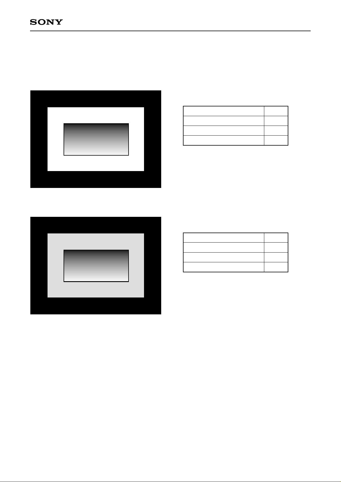
(10) Ve rtical ramp
When PG_PAT[2:0] = 7h and PG_STAIR_SW = 0, a vertical ramp is displayed.
The signal level is incremented from 000h by one bit for each line.
CXD3511Q
PG_SIG2R (G, B)
PG_SIG1R (G, B)
PG_R (G, B)_SEL
PG_PAT[2:0]
PG_STRP_SW
PG_STAIR_SW
PG_R (G, B)_SEL
PG_PAT[2:0]
PG_STRP_SW
PG_STAIR_SW
0
7h
x
0
1
7h
x
0
– 30 –
x: Don't care
Page 31
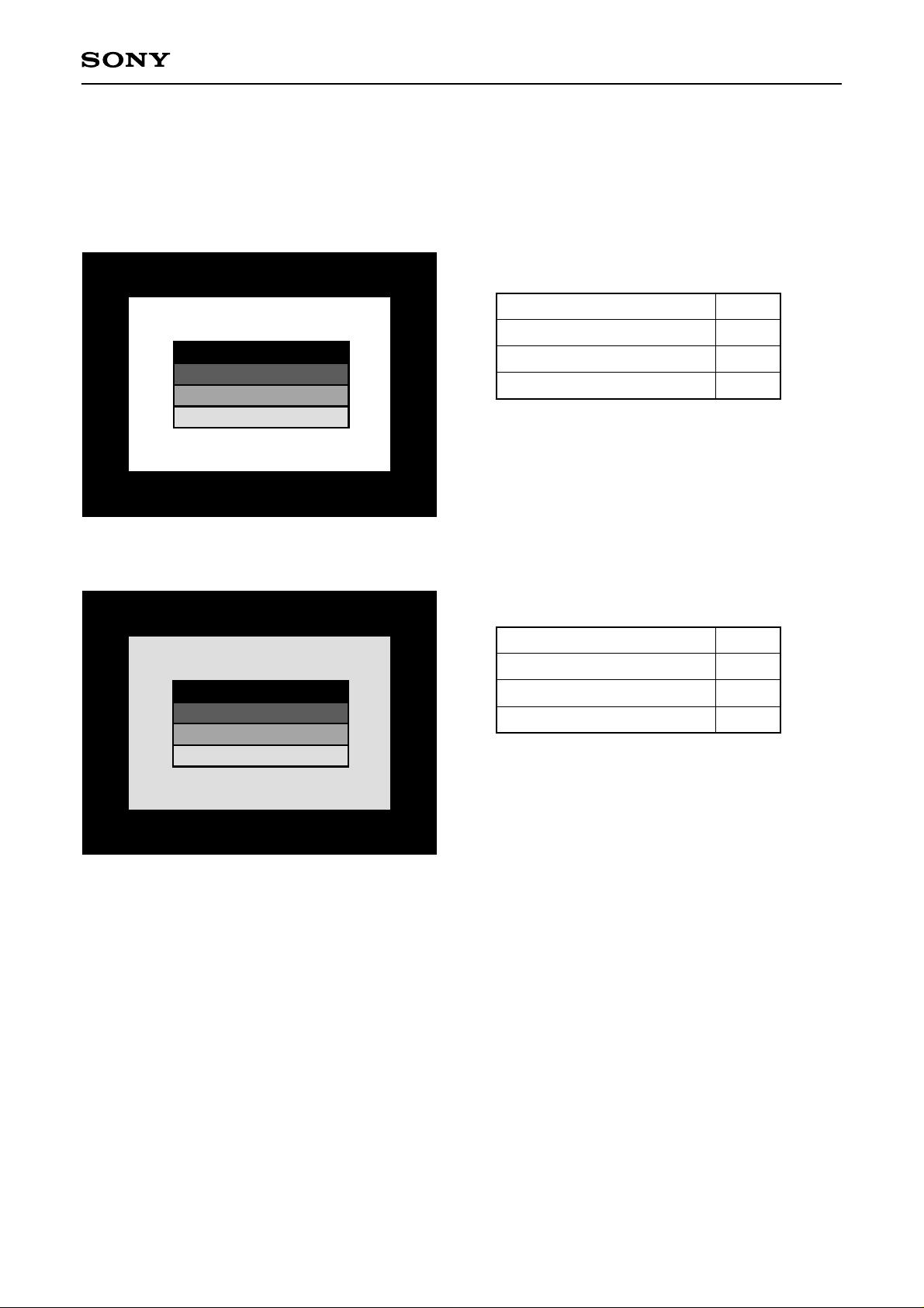
(11) V ertical stair
When PG_PAT[2:0] = 7h and PG_STAIR_SW = 1, a vertical stair is displayed.
The signal level is incremented from 000h by 64 bits for each 32 lines.
CXD3511Q
PG_SIG2R (G, B)
PG_SIG1R (G, B)
PG_R (G, B)_SEL
PG_PAT[2:0]
PG_STRP_SW
PG_STAIR_SW
PG_R (G, B)_SEL
PG_PAT[2:0]
PG_STRP_SW
PG_STAIR_SW
0
7h
x
1
1
7h
x
1
– 31 –
x: Don't care
Page 32
CXD3511Q
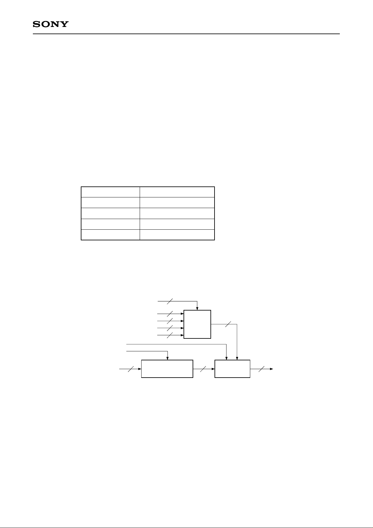
(k) OSD block
This block performs video signal half-tone processing and OSD-MIX processing by inputting the 2-bit OSD
signal for each color and the YS and YM signals. The half-tone processing setting is as follows.
YM signal input: 1 = Half tone processing ON, 0 = OFF
Here, the video signal level is halved by shifting the input data by one bit to the LSB side when YM = 1. For
example, when 0F0h is input, 078h is output.
The selector selects one of four types of data with respect to the OSD signal value as shown in the table
below. The selected data becomes the OSD signal scale data. The selected scale data can be set
independently in 10 bits for R, G and B, so 4 scales can be selected as desired from among 1024 scales for
each of R, G and B. Therefore, the desired 64 (= 2^6) colors can be selected from among the total 1.07374
billion (= 2^30) colors for R, G and B.
OSD signal input
0h
1h
2h
3h
Selected scale data
R, G, B_OSD_DAT1
R, G, B_OSD_DAT2
R, G, B_OSD_DAT3
R, G, B_OSD_DAT4
The OSD-MIX processing setting is as follows.
YS signal input: 1 = OSD-MIX processing ON, 0 = OFF
OSD signal
Scale data (R, G, B_OSD_DAT1)
Scale data (R, G, B_OSD_DAT2)
Scale data (R, G, B_OSD_DAT3)
Scale data (R, G, B_OSD_DAT4)
YS signal
YM signal
10 10 10
Input
2
10
10
10
10
Selector
10
OSD-MIXHalf tone processing
Output
– 32 –
Page 33
CXD3511Q
(l) Gamma block
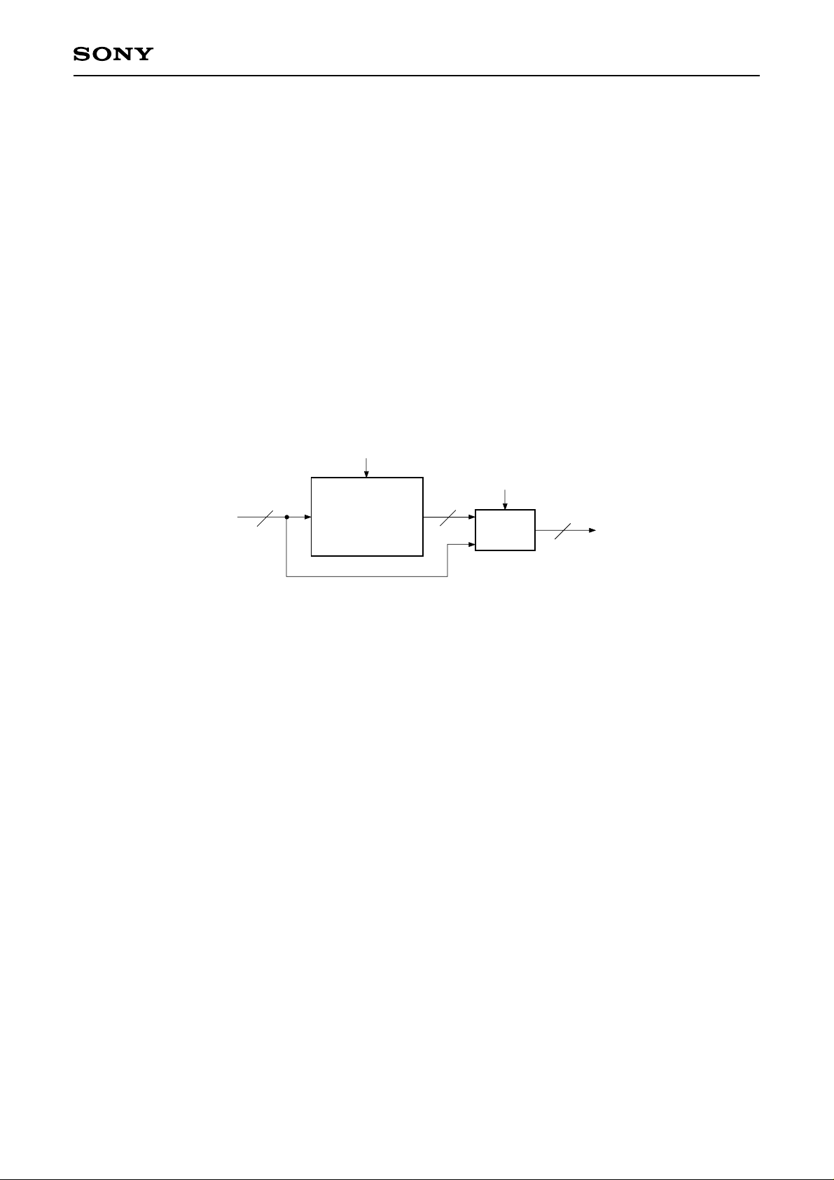
This block performs gamma correction for the user- and white balance-adjusted signal. Gamma correction
uses the LUT system, and the RAM size is 10 bits × 1024 words. The settings are as follows.
GAM_ON: 1 = Normal operation, 0 = Standby mode
GAM_SEL: 1 = Path passing through the RAM, 0 = Path not passing through the RAM
(All settings shared by R, G and B)
When operating the RAM, be sure to set GAM_ON = 1. Data cannot be written to or read from the RAM in
standby mode. The RAM data is set through the parallel I/F block.
Note that the RAM output is undetermined while data is being set in this RAM, and also during power-on.
RAM ON/OFF
(GAM_ON)
Select signal
(GAM_SEL)
Input
10
RAM
10 bits × 1024 words
10
10
OutputSelector
– 33 –
Page 34
CXD3511Q
(m) Color shading correction block
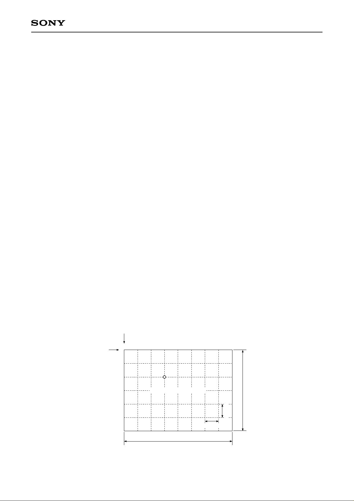
This block corrects color shading by adding a correction signal to the video signal. Correction points are set at
fixed intervals in the horizontal, vertical and scale directions of the video signal. The correction data for these
correction points is written in the RAM, and a smooth correction curve is created by reading this data and
performing interpolation operations. The settings are as follows.
CSC_ON: 1 = Color shading correction processing ON, 0 = processing OFF
CSC_H_MODE: Sets the horizontal correction interval to 32, 64 or 128 dots
CSC_V_MODE: Sets the vertical correction interval to 32, 64 or 128 lines
CSC_G_MODE: 1 = Scale correction processing ON, 0 = processing OFF
CSC_HNUM: Sets the number of horizontal correction points
CSC_VNUM: Sets the number of vertical correction points
CSC_HP: Sets the horizontal correction start position in 2-dot units
CSC_VP: Sets the vertical correction start position in 1-line units
CSC_R (G, B)_RGT: 1 = Reflects the TG block RGT setting,
0 = Reflects the inverse of the TG block RGT setting
CSC_DWN: 1 = Reflects the TG block DWN setting,
0 = Reflects the inverse of the TG block DWN setting
CSC_XH_ON: 1 = Cross hatch insertion ON, 0 = OFF
(All settings except CSC_R (G, B)_RGT shared by R, G and B)
The RAM size is 8 bits × 520 words, so up to 520 correction points can be set. The correction data is set as
8-bit data with code. Correction data can be set in the range of –128 to +127 scale. The example shown in the
figure below is for a 1024-dot × 768-line XGA video signal divided into 9 points at 128-dot intervals in the
horizontal direction and 7 points at 128-line intervals in the vertical direction. The relationship between the
correction point coordinates (m, n) and the RAM address is obtained as follows.
RAM address = (m – 1) + (n – 1) × (Number of horizontal correction points)
For the example in the figure below, this is as follows.
(9 – 1) + (7 – 1) × 9 = 62
Thus, the correction data must be set in the RAM from address 0 to address 62.
Up/down and/or right/left inversion of the LCD panel is supported by controlling the method of reading the
correction data set in the RAM. Up/down and/or right/left inversion are set from DWN and RGT of the TG block.
CSC_DWN and CSC_R (G, B)_RGT control the linking with the TG block settings.
Horizontal correction start position
Vertical correction start position
12
1
2
3
4
5
3456789
(m, n)
Color shading correction range
768 lines
6
128 dots
7
1024 dots
128 lines
– 34 –
Page 35
CXD3511Q
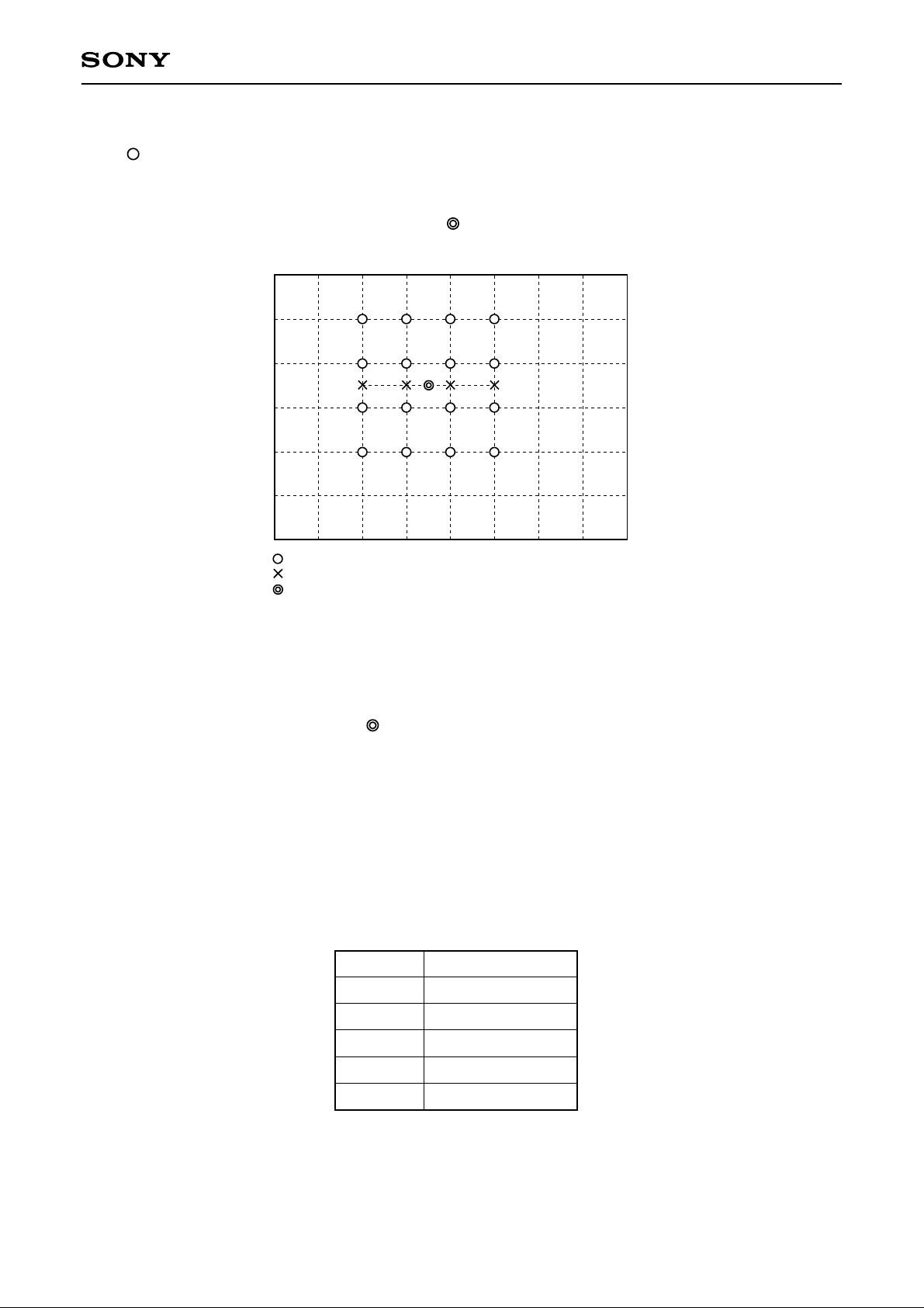
Interpolation operations in the horizontal and vertical directions are performed using the 16 points of correction
data ( marks in the figure below) around the pixel to be corrected. First, interpolation operations are
performed in the vertical direction using two upper and lower points of correction data at a time to obtain four
data (× marks in the figure below). Next, interpolation operations are performed in the horizontal direction
using these data to obtain the final correction data ( mark in the figure below).
12
1
2
3
4
5
6
7
: Correction data set in the RAM
: Vertical interpolation operation results
: Horizontal interpolation operation result
3456789
Interpolation operations in the scale direction are performed using the correction data in the five RAMs. When
CSC_G_MODE = 1, interpolation operations are performed in the scale direction. There are 5 correction points
in the scale direction. The data set in RAM1 to RAM5 is treated as each scale level correction data as shown
in the table below, and interpolation operations are performed in the horizontal and vertical directions for each
RAM. Then the four operation results ( mark in the figure above) for that same pixel (coordinates) are
selected according to the scale level of the video signal input to the color shading correction block, and
interpolation operations are performed in the scale direction. Thus, when interpolation operations are
performed in the scale direction, the correction data for each pixel is obtained from a total 64 points of
correction data.
When CSC_G_MODE = 0, correction operations are not performed in the scale direction, and the correction
data calculated using the data set in RAM1 is reflected to all scales.
The calculated correction data is added to the video signal. If these operation results overflow or underflow,
clipping is performed and 3FFh or 000h is output.
RAM name
RAM1
RAM2
RAM3
RAM4
RAM5
Corresponding scale
3FFh
300h
200h
100h
000h
– 35 –
Page 36
CXD3511Q
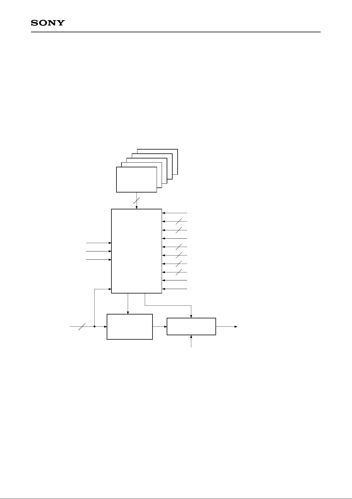
This block has a function for inserting the cross hatch that links the correction points into the video signal.
When CSC_XH_ON = 1, the cross hatch is inserted. The cross hatch level is 3FFh.
When CSC_XH_ON = 0, the cross hatch is not inserted.
The color shading correction block RAM output is undetermined during power-on. When performing color
shading correction, be sure to set data in these RAMs. When performing color shading correction in only the
horizontal and vertical directions, be sure to set CSC_ON = 1 before setting data in RAM1 of each color. When
performing color shading correction in the scale direction in addition to the horizontal and vertical directions,
set CSC_ON = 1 and CSC_G_MODE = 1 before setting data in RAM1 to RAM5 of each color. When CSC_ON
= 0 and CSC_G_MODE = 0, the RAMs are in standby mode and data cannot be set.
RAM5
RAM4
RAM3
RAM2
RAM1
8 bits × 520 words
8 × 5
Processing ON/OFF (CSC_ON)
2
Horizontal correction interval (CSC_H_MODE)
2
Vertical correction interval (CSC_V_MODE)
Internal HD
Internal VD
Internal MCLK
Correction
signal
Input Output
10
Interpolation
processing
Cross hatch
Addition/subtraction
and
clipping
10
10
10
10
Cross hatch insertion
Cross hatch ON/OFF
Number of scale correction points (CSC_G_MODE)
Number of horizontal correction points (CSC_HNUM)
Number of vertical correction points (CSC_VNUM)
Horizontal correction start position (CSC_HP)
Vertical correction start position (CSC_VP)
Left/right inversion (CSC_R(G,B)_RGT)
Up/down inversion (CSC_DWN)
(CSC_XH_ON)
– 36 –
Page 37
CXD3511Q
(n) Selectable delay line block
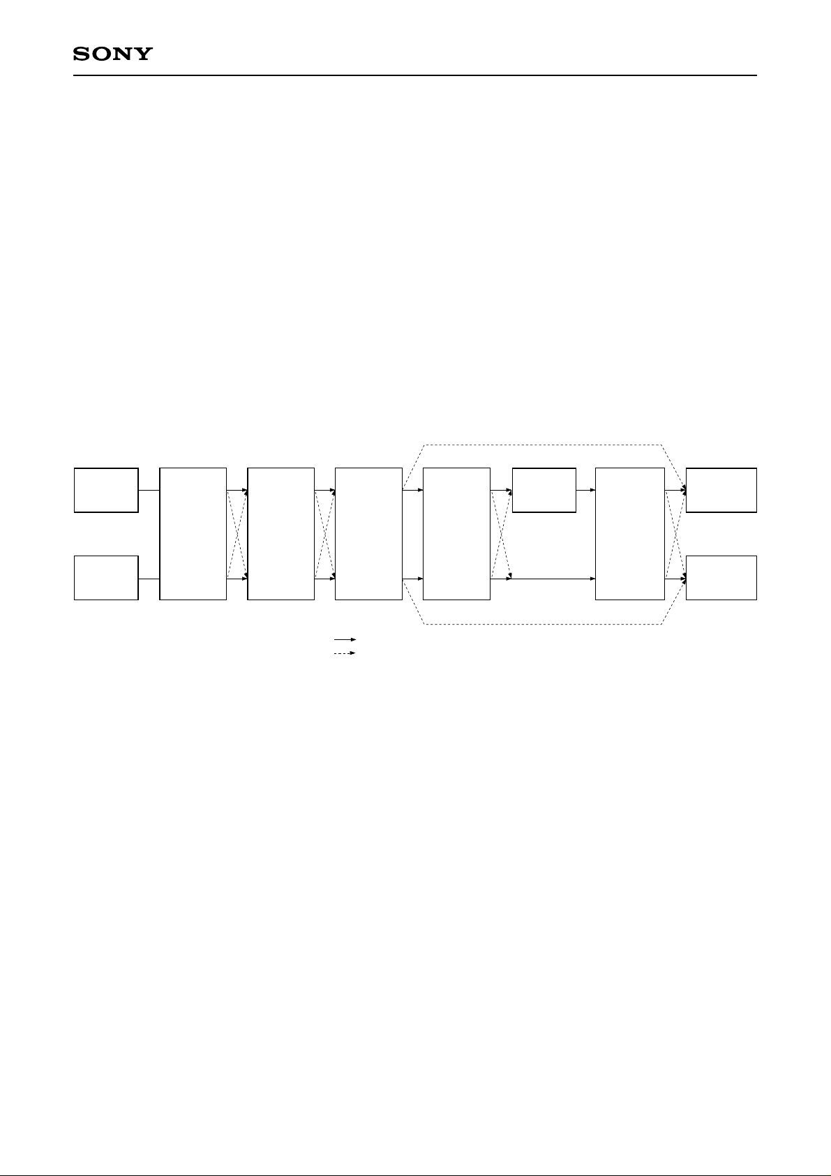
This block supports signal shifting in 1-dot units, performs signal port switching linked with right/left inversion
and signal processing that supports dot/line inversion.
This block is comprised of five selectors: dot shift selector, right/left inversion selector, dot/line selector, up/
down inversion pre-selector, and up/down inversion post-selector.
The delay line size is 1200 words.
The data paths for this block are shown in the figure below. Port switching during right/left inversion depends
on the Cond1 value, and port switching during up/down inversion (when dot/line inversion support is ON)
depends on the Cond2 value.
Cond1 = (RGT_SEL_ON) AND [(RGT) Ex-NOR (DLY_R (G, B)_RGT)]
Cond2 = (DWN) Ex-NOR (DLY_DWN)
Note) RGT and DWN are TG block settings.
Input port 1
Input port 2
Dot shift
selector
HP[0]
Right/left
inversion
selector
Cond1
Dot/line
selector
DLY_ON
Solid lines: 1
Dotted lines: 0
Up/down
inversion
pre-selector
Cond2
Delay line
Output port 1
Up/down
inversion
post-selector
Cond2
Output port 2
– 37 –
Page 38

(1) 1-dot shift
When HP[0] = 0, the output data is delayed by one dot compared to when HP[0] = 1.
clk
CXD3511Q
port1 in
port2 in
port1 out
port2 out
1.0 1.2 1.4 1.6 1.8 1.10 1.12 1.14 1.16 1.18
1.1 1.3 1.5 1.7 1.9 1.11 1.13 1.15 1.17 1.19
1.1 1.3 1.5 1.7 1.9 1.11 1.13 1.15
1.0 1.2 1.4 1.6 1.8 1.10 1.12 1.14 1.16
(2) Right/left inversion
When Cond1 = 0, signal port switching is performed for the output data.
clk
port1 in
port2 in
port1 out
1.0 1.2 1.4 1.6 1.8 1.10 1.12 1.14 1.16 1.18
1.1 1.3 1.5 1.7 1.9 1.11 1.13 1.15 1.17 1.19
1.1 1.3 1.5 1.7 1.9 1.11 1.13 1.15 1.17
IN2
port2 out
1.0 1.2 1.4 1.6 1.8 1.10 1.12 1.14 1.16
– 38 –
IN1
Page 39
CXD3511Q
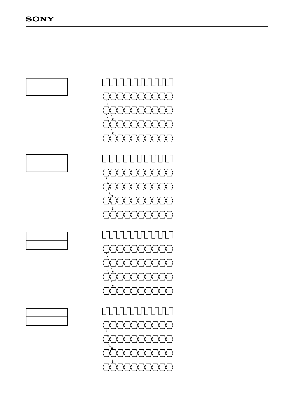
(3) Dot/line inversion support
When DLY_ON = 1, signal processing that supports dot/line inverted dr ive is performed. The output data is
output as shown in the figures below according to the Cond1 and Cond2 values. D and the dotted lines in the
figures indicate that the signal is delayed by 1H.
Cond1
1
Cond1
0
Cond2
1
Cond2
1
clk
port1 in
port2 in
port1 out
port2 out
clk
port1 in
port2 in
port1 out
port2 out
1.0 1.2 1.4 1.6 1.8 1.10 1.12 1.14 1.16 1.18
1.1 1.3 1.5 1.7 1.9 1.11 1.13 1.15 1.17 1.19
0.0 0.2 0.4 0.6 0.8 0.10 0.12 0.14 0.16
1.1 1.3 1.5 1.7 1.9 1.11 1.13 1.15 1.17
1.0 1.2 1.4 1.6 1.8 1.10 1.12 1.14 1.16 1.18
1.1 1.3 1.5 1.7 1.9 1.11 1.13 1.15 1.17 1.19
0.1 0.3 0.5 0.7 0.9 0.11 0.13 0.15 0.17
1.0 1.2 1.4 1.6 1.8 1.10 1.12 1.14 1.16
D1
IN2
D2
IN1
Cond1
1
Cond1
0
Cond2
0
Cond2
0
clk
port1 in
port2 in
port1 out
port2 out
clk
port1 in
port2 in
port1 out
port2 out
1.0 1.2 1.4 1.6 1.8 1.10 1.12 1.14 1.16 1.18
1.1 1.3 1.5 1.7 1.9 1.11 1.13 1.15 1.17 1.19
1.0 1.2 1.4 1.6 1.8 1.10 1.12 1.14 1.16
0.1 0.3 0.5 0.7 0.9 0.11 0.13 0.15 0.17
1.0 1.2 1.4 1.6 1.8 1.10 1.12 1.14 1.16 1.18
1.1 1.3 1.5 1.7 1.9 1.11 1.13 1.15 1.17 1.19
1.1 1.3 1.5 1.7 1.9 1.11 1.13 1.15 1.17
0.0 0.2 0.4 0.6 0.8 0.10 0.12 0.14 0.16
– 39 –
IN1
D2
IN2
D1
Page 40
CXD3511Q
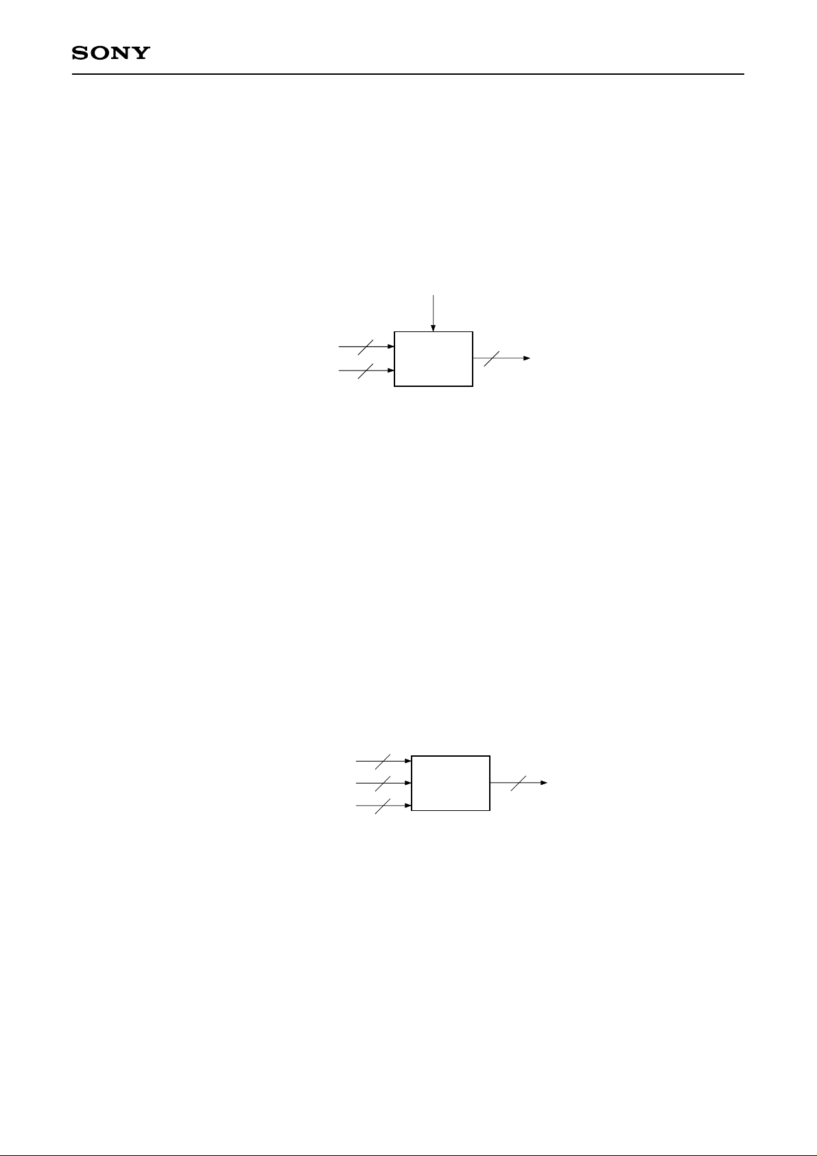
(o) Mute 2 block
This block performs mute processing by replacing the video signal with data of the desired level. The settings
are as follows.
MUTE2_ON: 1 = Mute processing ON, 0 = OFF (Setting shared by R, G and B)
R, G, B_MUTE2: RGB mute data (Set independently for R, G and B)
Select data (MUTE2_ON)
Input
Coefficient
(R, G, B_MUTE2)
10
10
Selector
10
Output
(p) Limiter block
This block performs limiter processing so that the output signal does not exceed a certain range. The settings
are as follows.
L_LIM_DAT: Low side limiter level
When input data ≤ L_LIM_DAT, the output is clipped to L_LIM_DAT.
H_LIM_DAT: High side limiter level
When H_LIM_DAT ≤ input data, the output is clipped to H_LIM_DAT.
(Both settings shared by R, G and B)
Set data so that the relationship L_LIM_DAT < H_LIM_DAT is constantly maintained. When both coefficient
values are 000h, limiter processing is not performed.
Input
Coefficient (H_LIM_DAT)
Coefficient (L_LIM_DAT)
10
10
10
– 40 –
Limiter
10
Output
Page 41
CXD3511Q
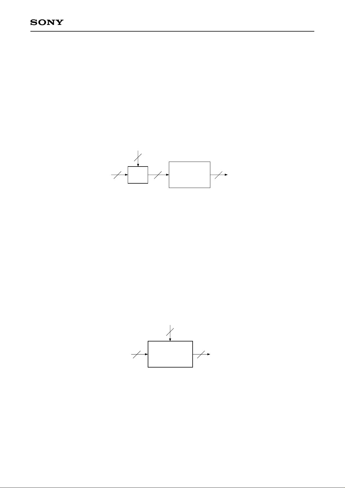
(q) Post gain block
This block performs multiplication processing independently for ports 1 and 2. The settings are as follows.
Coefficient: 8 bits
Gain setting: 0 to 1.9921875 (= 255/128) times, variable in 256 steps
(Set independently for R, G and B ports 1 and 2)
Multiplication is performed using the 10-bit input and an 8-bit coefficient, and the upper 12 bits c[17:6] of the
operation results are output. Next, the c[6] value is checked and rounding is performed to 11 bits. The MSB of
the rounded 11 bits is checked, clipping is performed, and the lower 10 bits are output.
Coefficient
b[7:0]
Input
a[9:0]
8
a × b
1210
c[17:6]
Rounding
and
clipping
10
Output
(r) Post bright block
This block performs addition and subtraction processing independently for ports 1 and 2. The settings are as
follows.
Coefficient: 7 bits with code, MSB = code bit
Bright setting: –64 to +63 scales, variable with an accuracy of 1 bit
(Set independently for R, G and B ports 1 and 2)
Multiplication is performed using the 10-bit input and a 7-bit coefficient with code. The coefficient MSB is the
code bit. Addition is performed when b[6] = 0, and subtraction when b[6] = 1. However, when performing
subtraction, set the two's complement in the lower bits of the coefficient. When the operation results overflow
or underflow, clipping is performed.
Input
a[9:0]
10
Coefficient
b[6:0]
7
Addition/subtraction
and
clipping
– 41 –
10
Output
Page 42
CXD3511Q
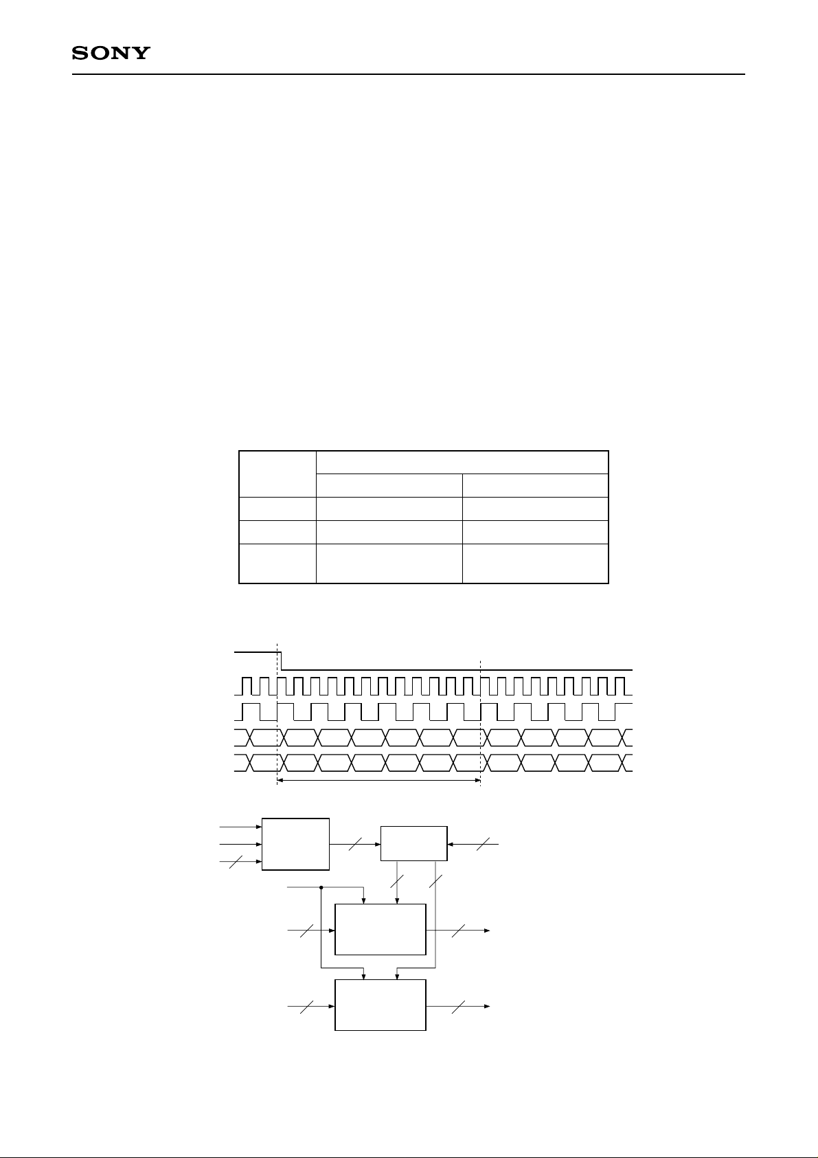
(s) Cycle offset block
This block performs addition and subtraction processing independently for ports 1 and 2. Arithmetic
coefficients are selected sequentially using the counter output value as the select signal. Therefore, a cyclic
offset relative to the video signal can be attached. The settings are as follows.
OFFSET_ON: 1 = Offset processing ON, 0 = OFF (Setting shared by R, G and B)
OFFSET_MODE: 0h = 6-dot period, 1h = 12-dot period, 2h = 24-dot period (Setting shared by R, G
and B)
R, G, B_OFFSET1 to R, G, B_OFFSET24: 5-bit offset data with code
–16 to +15 scales, variable with an accuracy of 1 bit
(Set independently for R, G and B)
The coefficients selected according to the counter operating period are as shown in the table below. In all
cases, the coefficients are assigned in ascending order from the smallest number. The coefficient MSB is the
code bit. Addition is performed when MSB = 0, and subtraction when MSB = 1. However, when performing
subtraction, set the two's complement in the lower bits of the coefficient. When the operation results overflow
or underflow, clipping is performed.
Period
6 dots
12 dots
24 dots
Port 1 side
1, 3, 5
1, 3, 5, 7, 9, 11
1, 3, 5, 7, 9, 11, 13,
15, 17, 19, 21, 23
Port 2 side
2, 4, 6
2, 4, 6, 8, 10, 12
1, 4, 6, 8, 10, 12, 14,
16, 18, 20, 22, 24
The counter reset timing is delayed by 12 dot clocks from the front edge of the HDIN input.
HDIN input (negative polarity)
Dot clock
1/2 frequency-divided clock
Coefficient number output from selector
R1, G1, B1OUT
R2, G2, B2OUT
Internal HD
Internal MCLK
OFFSET_MODE
2
OFFSET_ON
12 clocks
Counter Selector
4
55
5 × 24
1357
2468
Coefficient (R, G, B_OFFSET1 to R, G, B_OFFSET24)
Input (port 1)
Input (port 2)
10
10
Addition/subtraction
and
clipping
Addition/subtraction
and
clipping
10
10
Output (port 1)
Output (port 2)
– 42 –
Page 43
CXD3511Q
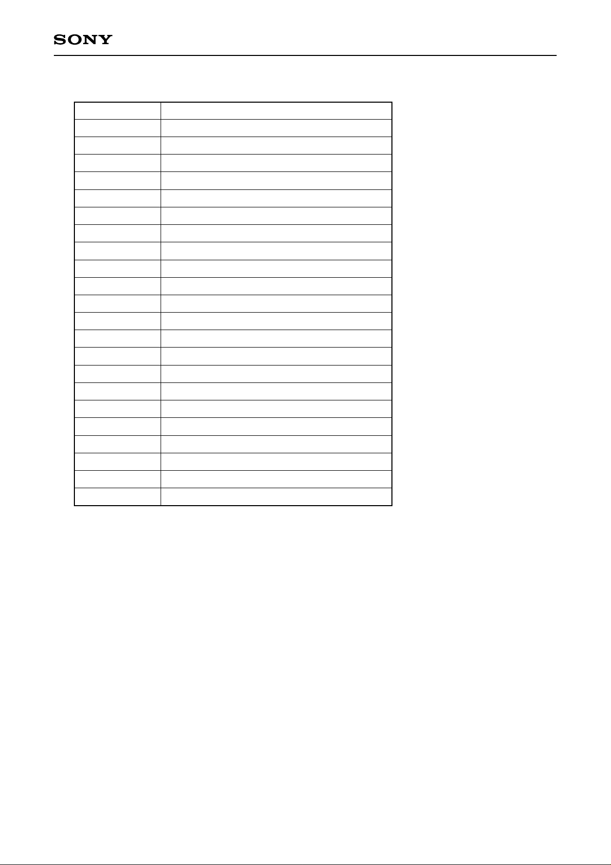
4. Timing Generator (TG) Block
This block generates the timing pulses required to drive Sony LCD panels. Of the output pulses, the required
pulses differ according to the LCD panel type, so be sure to also check the specifications of the panel used.
The output timing pulses are all set by the parallel I/F. For a detailed description, see the description of the
parallel I/F TG block.
The TG block diagram is shown below.
HDIN
VDIN
Parallel I/F
HSYNC Detect
VSYNC Detect VP Counter
PLL Counter HP Counter
INT_HDINT_VD
Control Register
HRS
H Pulse 2
Generator
H Pulse 1
Generator
V Pulse Generator
HST, PST, HCK1, HCK2,
DCK1, DCK1X, DCK2,
DCK2X, ENBR, ENBL,
DENB, PCG, PRG,
SHST, HD2
CLP, HD1
VSTR, VSTL, VCKR,
VCKL, FRP, XFRP,
BLK
CTRL
RGT, DWN
XRGT, PO1, 2, 3, 4, 5
Timing Generator Block Diagram
– 43 –
Page 44

CXD3511Q
5. Parallel I/F Block
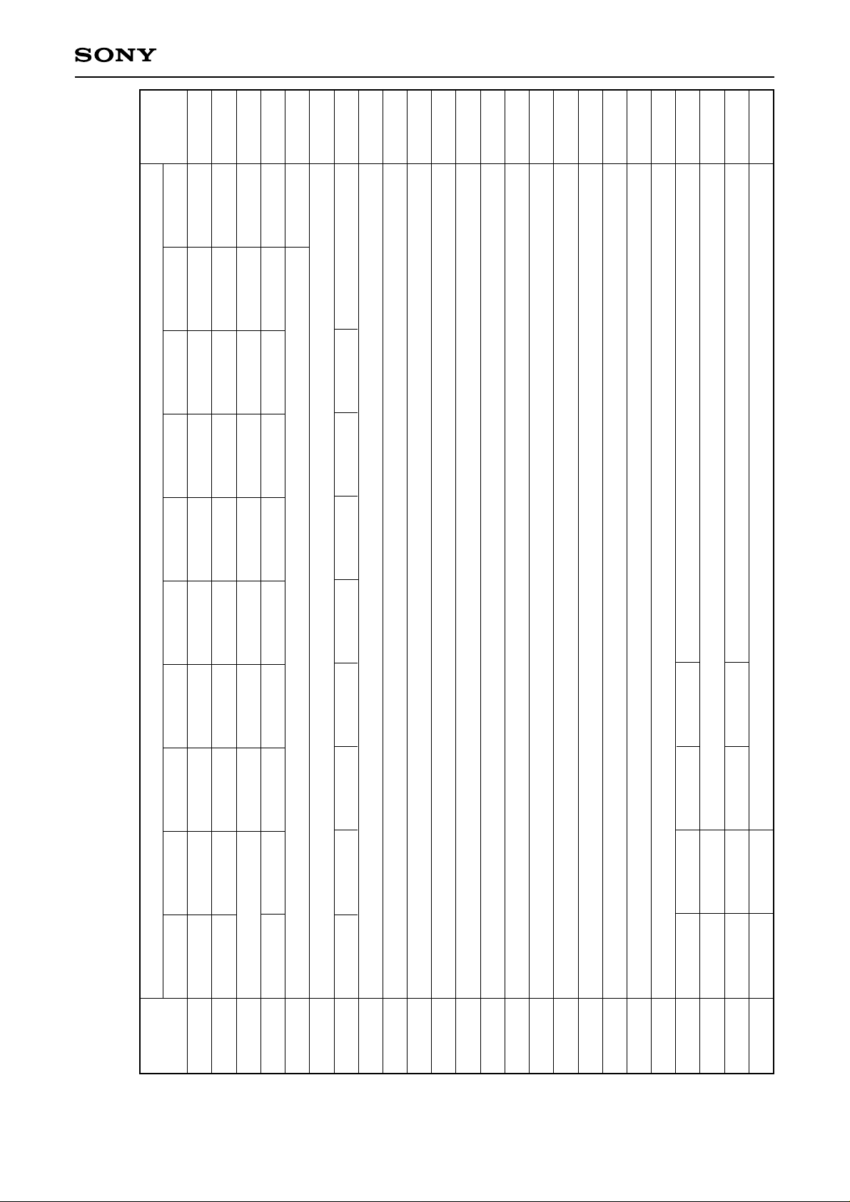
Register data settings in this IC are performed by parallel data. As shown in the Timing Chart below, the parallel
I/F comprises a total 12-bit wide bus consisting of control signal PCTL (Pin 12), clock signal PCLK (Pin 13) and
10-bit wide data signal PDAT[9:0] (Pins 14 to 17, 20 to 24 and 26).
The data signal is input in the order of main address, sub address and data. When setting data in this IC,
divide the data into 22 blocks as shown in the table on the next page. Next, the sub address specifies the initial
address of the data to be written in the block designated by the main address. The data is set sequentially from
the data at the address designated by the sub address. The address of each data set thereafter is
automatically incremented by +1 from the address designated by the sub address, so further address setting
is unnecessary. This makes it possible to set only the necessary data from the desired address of the desired
block.
(1) Timing chart
PCTL (Pin 12)
PCTL (Pin 13)
PDAT[9:0]
(Pins 14 to 17, 20 to 24 and 26)
Main
Address
Sub
Address
Data
– 44 –
Page 45
(2) Main address table
Main address Set block
000h
CXD3511Q
TG block
001h
002h
003h
004h
005h
006h
007h
008h
009h
00Ah
00Bh
00Ch
00Dh
00Eh
00Fh
010h
011h
DSD1 block
DSD2 block
Gamma block (Red) RAM
Gamma block (Green) RAM
Gamma block (Blue) RAM
Color shading correction block (Red) RAM1
Color shading correction block (Red) RAM2
Color shading correction block (Red) RAM3
Color shading correction block (Red) RAM4
Color shading correction block (Red) RAM5
Color shading correction block (Green) RAM1
Color shading correction block (Green) RAM2
Color shading correction block (Green) RAM3
Color shading correction block (Green) RAM4
Color shading correction block (Green) RAM5
Color shading correction block (Blue) RAM1
Color shading correction block (Blue) RAM2
012h
013h
014h
015h
Color shading correction block (Blue) RAM3
Color shading correction block (Blue) RAM4
Color shading correction block (Blue) RAM5
Pattern generator block
– 45 –
Page 46
CXD3511Q
Initial value
PDAT0
000h
PO1
PO2
PO3
PO4
PO5
1FFh
3FFh
PSTM
BLKON
HSTM
BLKPOL
VCKFIX
VCKPOL
VSTFIX
VSTPOL
HCKFIX
HCKPOL
000h
3FFh
SLXBLK
PLLP[11]
FRVC1LNK
RGVLNK
—
—
000h
000h
000h
HP[11:10]
—
—
—
000h
000h
000h
000h
000h
000h
000h
000h
000h
000h
000h
000h
000h
000h
SHP[5:0]
HSTPC[7:0]
000h
000h
HSTPF[5:0]
PSTPC[7:0]
Data
PDAT8 PDAT7 PDAT6 PDAT5 PDAT4 PDAT3 PDAT2 PDAT1
PDAT9
DWN
HSTPOL
RGT
DCKPOL
HR
VPOL
HPOL
CLKPOL
—
POLDET
—
HSTFIX
—
DCKFIX
—
DCKFINV
—
FRPM[1:0]
—
PLLP[10:1]
VFRRN[10:2]
—
—
—
—
—
VP[9:0]
HP[9:0]
CLPU[10:1]
CLPD[10:1]
PRGU[10:1]
HD1U[10:1]
PRGD[10:1]
HD1D[10:1]
FRPP[10:1]
SHSTU[10:1]
SHSTD[10:1]
DENU[10:1]
DEND[10:1]
—
—
—
—
—
—
—
—
—
—
—
—
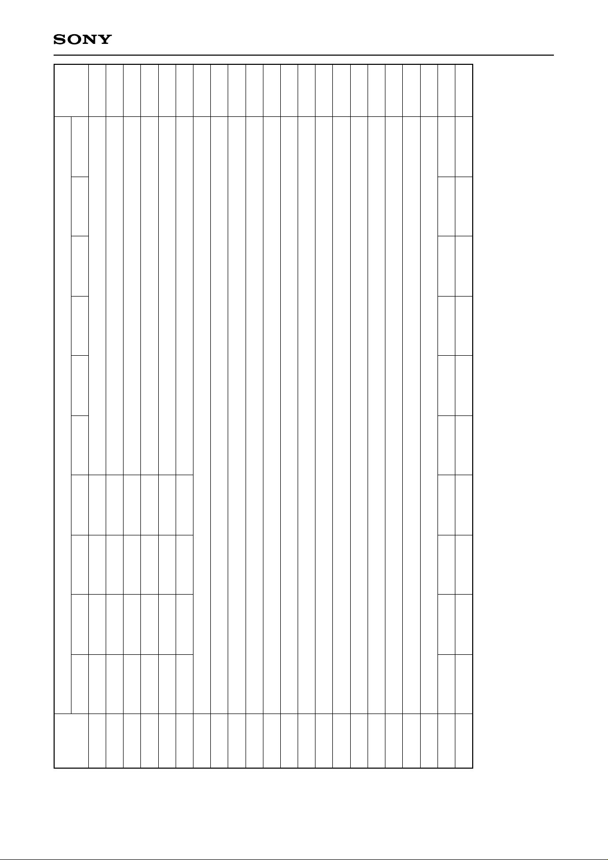
5-1. TG Block (Main Address: 000h)
The TG block data format is as follows.
000h
Sub address
001h
002h
003h
004h
005h
006h
007h
008h
– 46 –
009h
00Ah
00Bh
00Ch
00Dh
00Eh
00Fh
010h
011h
012h
013h
014h
015h
016h
017h
Page 47
Initial value
000h
000h
000h
000h
000h
000h
000h
000h
000h
000h
000h
000h
000h
000h
000h
000h
000h
000h
000h
000h
000h
CXD3511Q
000h
—: Don't care
Data
PDAT0
HCKC[5:0]
PSTPF[5:0]
DCK1F[5:0]
DCK2F[5:0]
DCK1W[5:0]
DCK2W[5:0]
PCGU[10:1]
PDGD[10:1]
ENB1U[10:1]
ENB1D[10:1]
ENB2U[10:1]
ENB2D[10:1]
VCK1P[10:1]
VST1P[11:2]
VCK2P[10:1]
HD2U[10:1]
VST2P[11:2]
HD2D[10:1]
BLKU[10:1]
BLKD[10:1]
BLKOE
XFRPOE
FRPOE
PCGOE
V2OE
DENOE
V1OE
SHSTOE
PRGOE
DCKXOE
—
—
—
PDAT8 PDAT7 PDAT6 PDAT5 PDAT4 PDAT3 PDAT2 PDAT1
—
PDAT9
018h
Sub address
—
—
—
—
019h
—
—
—
—
01Ah
—
—
—
—
01Bh
—
—
—
—
01Ch
—
—
—
—
01Dh
01Eh
01Fh
020h
021h
022h
023h
024h
– 47 –
025h
026h
027h
028h
029h
02Ah
02Bh
CLPOE
DCKOE
HD2OE
HCK2OE
HD1OE
HCK1OE
PSTOE
CLKOUT
—
HSTOE
02Ch
02Dh
Page 48
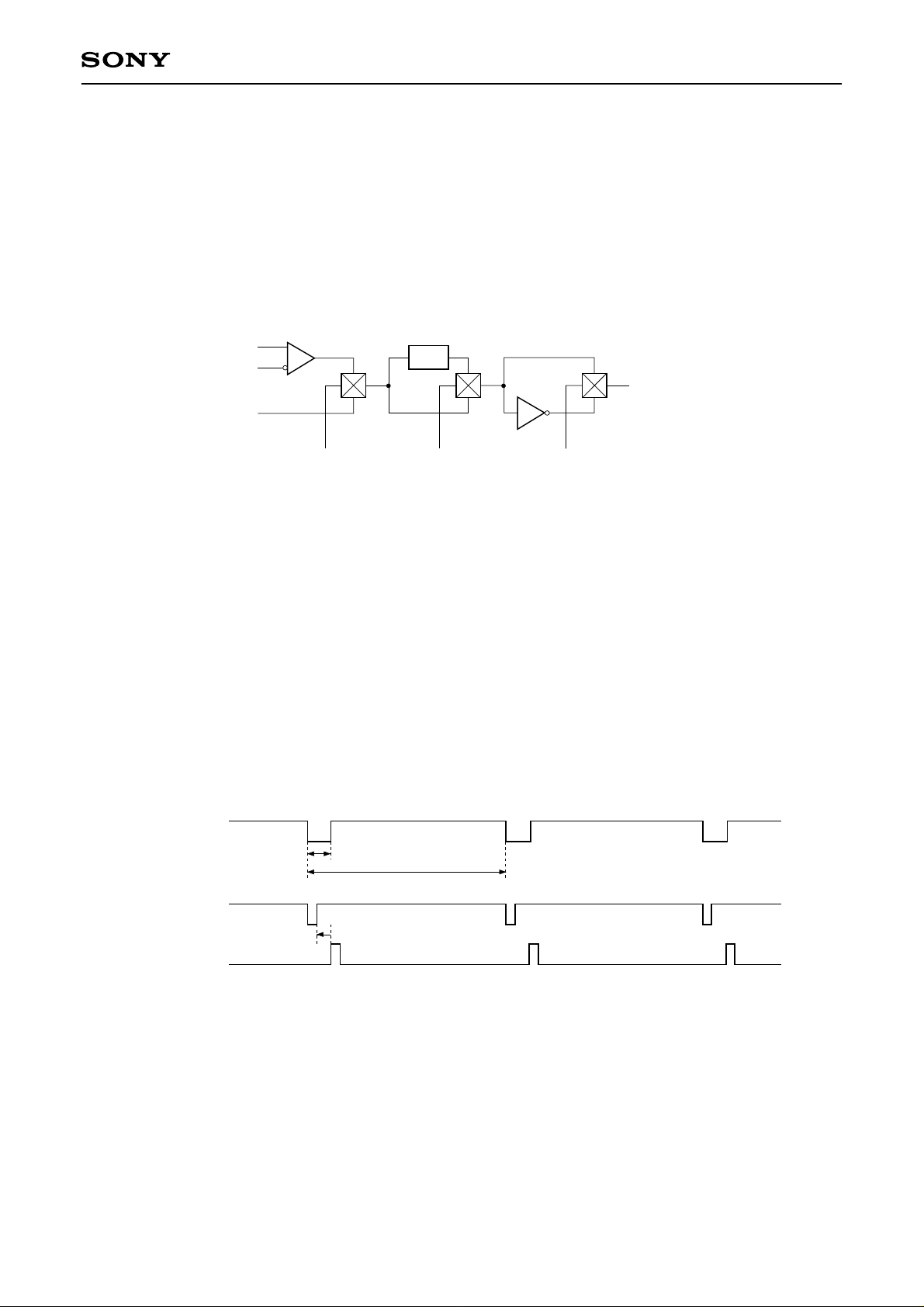
The detailed setting contents are described below.
(a) Clock settings
(1) CLKPOL (sub address: 000h)
This sets the internal clock polarity.
Setting value: 1 = Inverted, 0 = Not inverted
The clock flow from the clock input pins to the PLL block is shown below.
CXD3511Q
CLKP
CLKN
CLKC
CLKSEL1 CLKSEL2
1/2
To PLL Block
CLKPOL
(2) CLKOUT (sub address: 02Ch)
This sets the Pin 47 clock output limit.
Setting value: 1 = Inverted clock is output, 0 = Low is output
(b) SYNC polarity settings
(1) POLDET (sub address: 000h)
This sets the sync polarity auto discrimination function ON/OFF.
Setting value: 1 = Auto discrimination function ON, 0 = Auto discrimination function OFF
When POLDET = 1, the HPOL and VPOL settings below are invalid. When using this function, the HDIN sync
portion must be 1/2 or less of 1H, and the VDIN sync portion must come before the rise position of the VSTL/
R pulse.
HDIN (Negative)
N/2 or less
N
VDIN (Negative)
Must come before VSTL/R
VSTL/R
(2) HPOL and VPOL (sub address: 001h)
These set the sync signal polarity when POLDET = 0.
Setting value: 1 = Positive polarity, 0 = Negative polarity
The internal operation of this IC is with the input sync signal fixed to positive polarity. Therefore, these HPOL
and VPOL must be set in accordance with the polarity of the sync signal input from HDIN and VDIN.
Set HPOL and VPOL to "1" when the input sync signal is positive polarity, or to "0" when negative polarity.
– 48 –
Page 49

CXD3511Q
(c) Dots per 1H and lines per 1F settings
(1) HR (sub address: 000h)
This sets the PLL counter reset ON/OFF.
Setting value: 1 = Reset enabled, 0 = Reset disabled
When HR = 0, the internal frequency divider is used, and the HD1 pulse output should be used as the return
pulse. The number of dot clocks per 1H is set by PLLP[11:1] below.
(2) PLLP[11:1] (sub addresses: 004h and 005h)
This sets the internal PLL counter reset period in 11 bits. Setting is possible in 2-dot units. When the number of
dot clocks per 1H is N, set the "(N – 2)/2" value.
When HR = 0, free-running occurs at the above N. When HR = 1, if the next HDIN is not input before the
internal PLL counter counts up to 2047, free-running mode is established and free-running occurs at N.
When HDIN is input, free-running is canceled and normal operation is established.
(3) VFRRN[10:2] (sub address: 004h)
This sets the number of lines in 9 bits during vertical free running. Setting is possible in 4-line units. To have
operation run freely at M lines, set the "(M – 4)/4" value. If the next VDIN is not input before the internal vertical
line counter counts up to 2047, free-running mode is established. When VDIN is input, free-running is canceled
and normal operation is established.
(d) Scan direction settings
RGT and DWN (sub address: 000h)
These settings switch the scan directions of the LCD panel.
Setting value: 1 = Forward scan, 0 = Reverse scan
When CTRL (Pin 148) is low, RGT (Pin 136) and DWN (Pin 147) function as output pins, and the data set in
the respective registers is reflected. When CTRL is high, this setting is ignored, RGT and DWN function as
input pins, and are reflected to internal operation.
(e) Register parallel output settings
PO1, PO2, PO3, PO4 and PO5 (sub address: 000h)
These set the register setting parallel output.
Setting value: 1 = High is output, 0 = Low is output
The set data is reflected to the output pins PO1 (Pin 154), PO2 (Pin 153), PO3 (Pin 152), PO4 (Pin 164) and
PO5 (Pin 166) of the same name.
– 49 –
Page 50
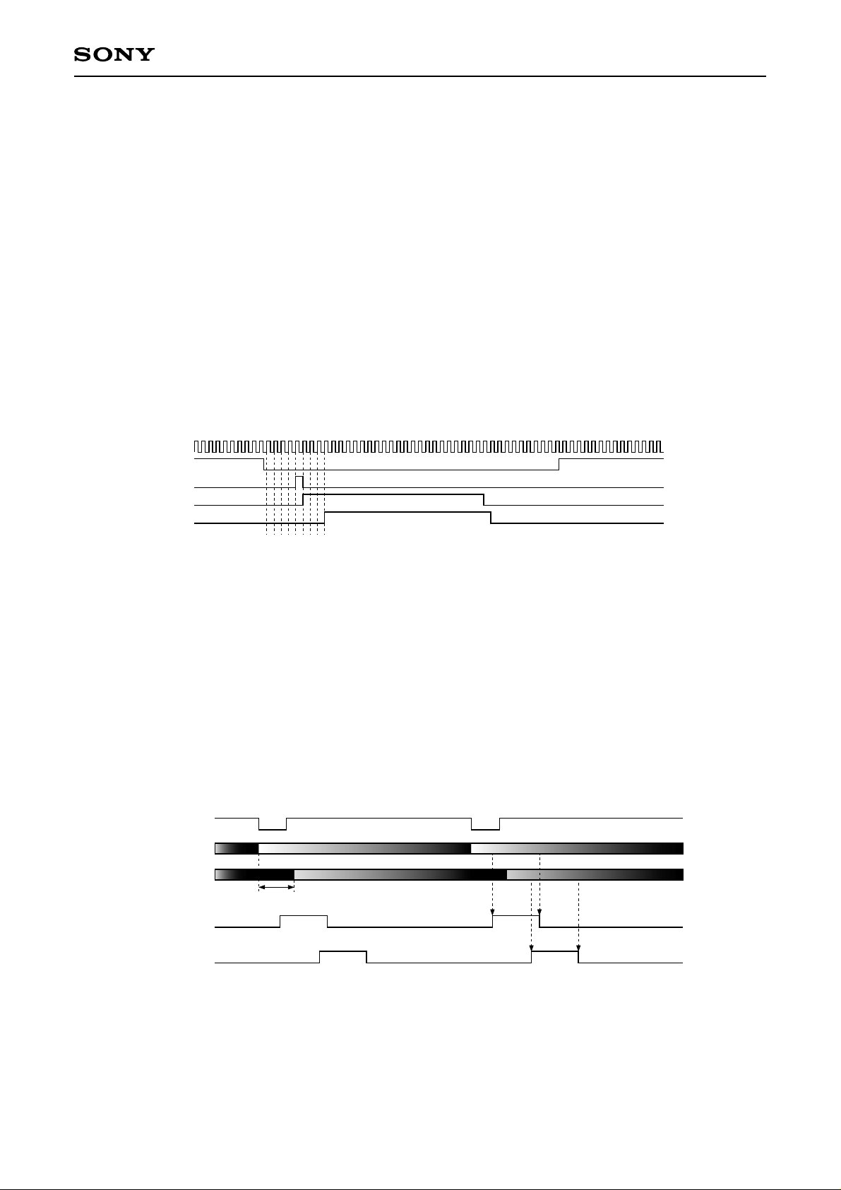
CXD3511Q
(f) Horizontal display position and horizontal direction pulse settings
(1) HP[11:0] (sub addresses: 006h and 007h)
HP[11:1] sets the horizontal pulse position for the LCD panel in 11 bits. The position can be set in 2-dot units
using the internal pulse INT_HD generated from the front edge of HDIN as the reference. The HP setting range
is from "0 to (N – 2)".
If the HP value is set to the number of frequency divisions N or higher, the HP setting is ignored and "(N – 2)"
is used as the setting value.
The HST, PST, HCK1, HCK2, DCK1, DCK1X, DCK2, DCK2X, ENBL, ENBR, VSTL, VSTR, VCKL, VCKR, FRP,
XFRP, PCG, PRG, BLK and HD2 horizontal timing pulses are linked according to the HP setting.
The internal reference pulse INT_HD rises at the 5th clock from the front edge of the HDIN input, and all the
pulses are synchronized using this as the reference. Increasing HP shifts the output positions of the linked
pulses toward the rear of the time series. The example below shows the shortest output position from HDIN
when HP is set to 000h. (Note that the output position changes according to the settings in (2) below.)
HP[0] can shift the video in 1-dot units. See 3. Description of DSD Block Signal Processing Functions, (n)
Selectable delay line block, (1) 1-dot shift for a detailed description.
Internal CLK
HDIN
INT_HD
HD1
HD2
(2) CLPU[10:1], CLPD[10:1], PRGU[10:1], PRGD[10:1], HD1U[10:1], HD1D[10:1], SHSTU[10:1],
SHSTD[10:1], DENU[10:1], DEND[10:1], PCGU[10:1], PCGD[10:1], ENB1U[10:1], ENB1D[10:1],
ENB2U[10:1], ENB2D[10:1], HD2U[10:1], HD2D[10:1]
(sub addresses: 009h to 013h, 01Eh to 023h and 028h to 029h)
These set the horizontal timing pulse output positions in 10 bits. The respective rise and fall positions can be
set in 2-dot units. Settings ending in "U" set the rise position, and settings ending in "D" set the fall position.
Horizontal pulses are divided into the following two types.
(A) CLP and HD1 → Pulses synchronized to the PLL counter
Set the "(rise position/fall position – 10)/2" value.
(B) PRG, SHST, DEN, PCG, ENBL, ENBR and HD2 → Pulses synchronized to the HP counter
Set the "(rise position/fall position – HP setting value – 16)/2" value.
An outline of each type is shown below. When ∗∗U and ∗∗D are set to the same value, "1" is output.
HDIN
PLL counter
HP counter
(A)
(B)
0
HP[11:1]
0
0
0
∗∗
U
∗∗
D
∗∗
U
∗∗
D
(3) HD1OE, HD2OE, CLPOE, PRGOE, SHSTOE, DENOE and PCGOE (sub addresses: 02Ch and 02Dh)
These set the HD1, HD2, CLP, PRG, SHST, DEN and PCG pulse output limits, respectively.
Setting value: 1 = Pulse is output, 0 = Output is fixed to "0"
– 50 –
Page 51

CXD3511Q
(g) Vertical display position setting
VP[9:0] (sub address: 008h)
This sets the vertical display start position in 10 bits. The position can be set in 1-line units using the front edge
of VDIN as the reference. The VSTL/VSTR, VCKL/VCKR, FRP and XFRP pulse phases change by linking with
this setting.
Minimum
adjustment
width: 1H
VDIN
HDIN
VSTL
VCKL
Tvp
Tvp minimum and maximum setting values
VP[9:0]
Tvp
Min.
000h
6H
Max.
3FFh
1029H
– 51 –
Page 52
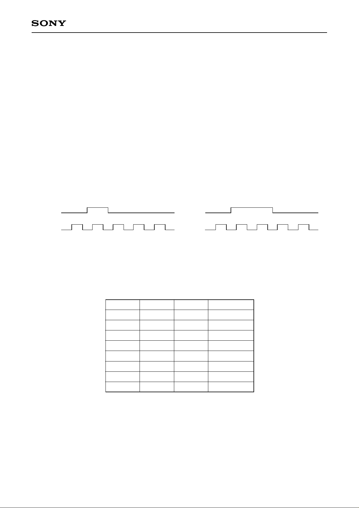
(h) HST and PST pulse settings
(1) HSTM (sub address: 002h)
This sets the pulse width for horizontal display start timing pulse HST.
Setting value: 1 = Twice the HCK per iod width, 0 = HCK per iod width
Set the width according to the LCD panel specifications.
(2) PSTM (sub address: 002h)
This sets the pulse width for dot sequential precharge start timing pulse PST.
Setting value: 1 = Twice the HCK per iod width, 0 = HCK per iod width
Set the width according to the LCD panel specifications.
CXD3511Q
HST, PST
HCK1
HSTM, PSTM = 0
HST, PST
HCK1
HSTM, PSTM = 1
(3) HSTFIX and HSTPOL (sub addresses: 001h and 002h)
These set the HST and PST pulse output polarities. The polarity changes as follows according to the
combination of linked/not linked with control signal RGT. This setting is shared by HST and PST.
HSTFIX
0
0
0
0
1
1
HSTPOL
0
0
1
1
0
0
RGT
0
1
0
1
0
1
Output polarity
Positive
Negative
Negative
Positive
Negative
Negative
1
1
1
1
0
1
Positive
Positive
– 52 –
Page 53
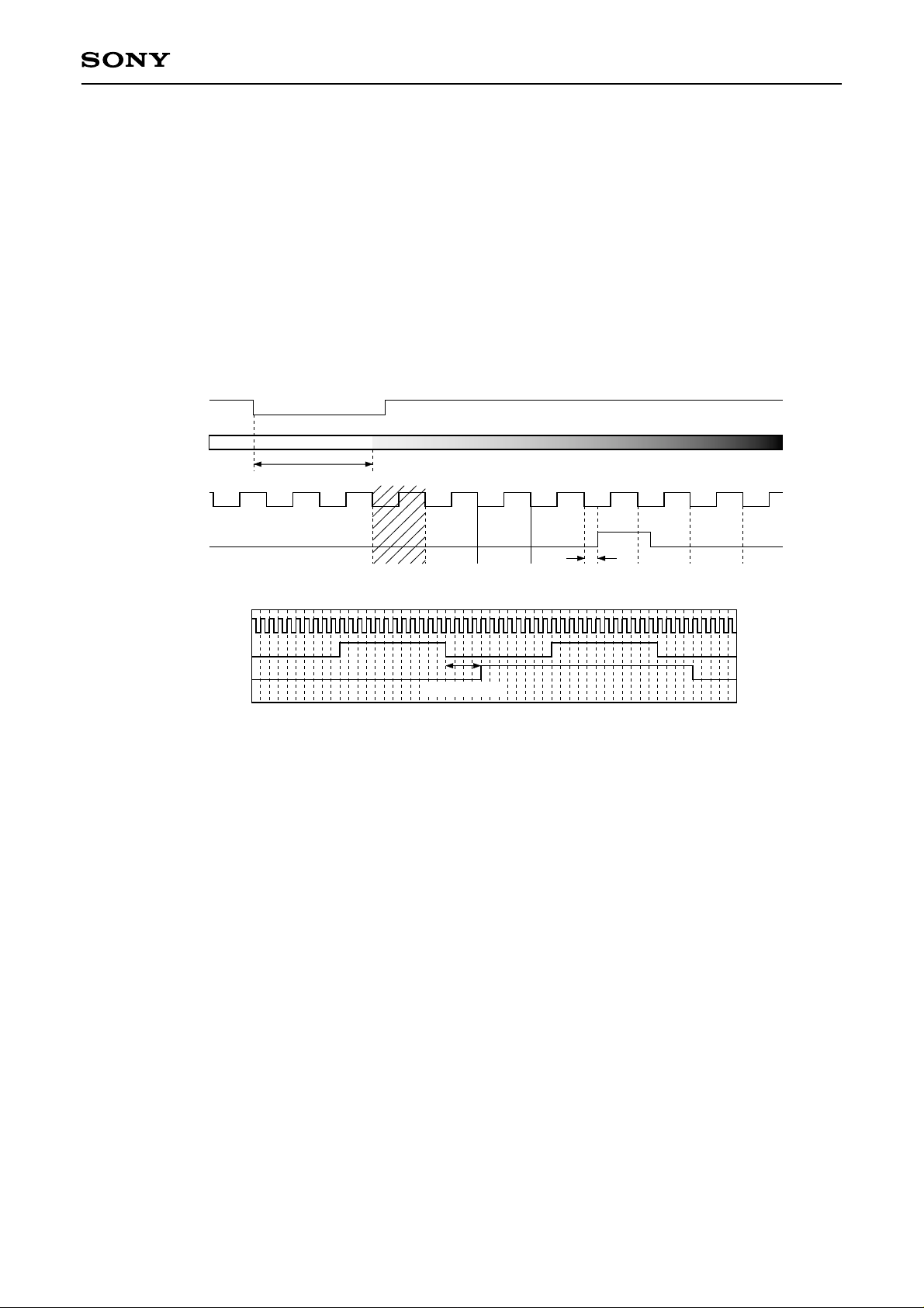
CXD3511Q
(4) HSTPC[7:0], HSTPF[5:0], PSTPC[7:0] and PSTPF[5:0] (sub addresses: 015h to 018h)
These set the HST and PST pulse phases. Reset is applied when the internal HP counter reaches "0", and the
HST and PST pulse phases within 1H can be set at the HCK1 and HCK2 period, respectively, by HSTPC and
PSTPC.
HSTPF and PSTPF can set the HST and PST pulse phase relative to HCK1 and HCK2 in 1-dot units.
Do not set HSTPC and PSTPC to 00h, as the pulses may not be output correctly in this case.
The HSTPF and PSTPF values can be set up to "(HCKC × 2 – 2)". If higher values are set, the pulses are not
output. Set the "(phase difference from HCK pulse)" value.
The figures below show the timings for HSTPC: 04h and HSTPF: 04h, respectively. These timings are the
same for the PST pulse.
HSYNC
0
HP counter
HP[11:0]
HCK1
10 234567
HST
Setting prohibited HSTPF[5:0]
MCLK
HCK1
HST
HSTPF: 04h
(5) HSTOE and PSTOE (sub address: 02Dh)
These set the HST and PST pulse output limits, respectively.
Setting value: 1 = Pulse is output, 0 = Output is fixed to "0"
– 53 –
Page 54
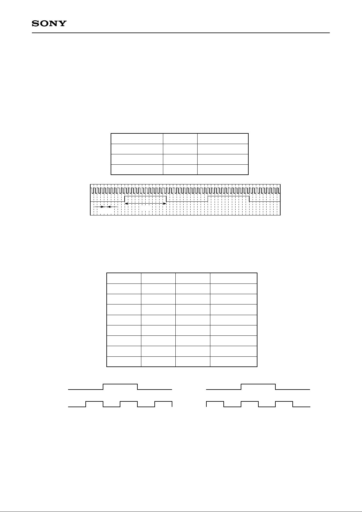
CXD3511Q
(i) HCK1 and HCK2 pulse settings
(1) HCKC[5:0] (sub address: 019h)
This sets the HCK1 and HCK2 period (LCD panel sampling period). Settings which result in an odd number for
Tckw in the figure below are prohibited, so be sure to set a value that results in an even number. Set the
"(Tckw – 1)" value according to the LCD panel specifications. When this setting is changed, the HST and PST
pulse phases also change, so first set HCKC to the correct value and then make the HST and PST settings.
Example setting values are shown in the table below.
MCLK
HCK1
1 clk
LCD panel
SVGA, WXGA
XGA, SXGA
UXGA
Tckw
Tckw
6 clk
12 clk
24 clk
HCKC setting
05h
0Bh
17h
(2) HCKFIX and HCKPOL (sub addresses: 001h and 002h)
These set the HCK pulse output polarity. The polarity relative to the HST pulse changes as follo ws according to
the combination of linked/not linked with control signal RGT.
HCKFIX
L
L
L
HCKPOL
L
L
H
RGT
L
H
L
Output polarity
Positive
Negative
Negative
L
H
H
H
H
Positive
HST
HCK1
H
L
L
H
H
H
L
H
L
H
HST
HCK1
(3) HCK1OE and HCK2OE (sub address: 02Dh)
These set the HCK1 and HCK2 pulse output limits, respectively.
Setting value: 1 = Pulse is output, 0 = Output is fixed to "0"
– 54 –
Positive
Negative
Negative
Positive
Positive
Negative
HSTPF[7:0] = 00h
Page 55
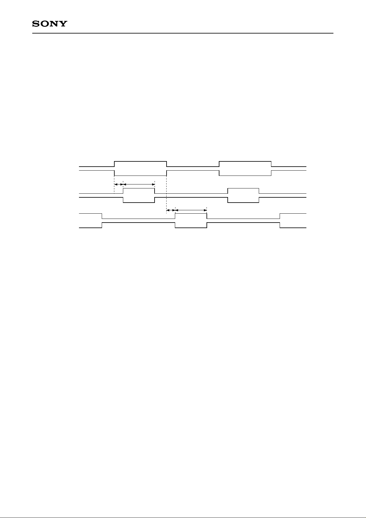
CXD3511Q
(j) DCK1, DCK1X, DCK2 and DCK2X pulse settings
(1) DCK1F[5:0], DCK1W[5:0], DCK2F[5:0] and DCK2W[5:0] (sub addresses: 01Ah to 01Dh)
These set the DCK1, DCK1X, DCK2 and DCK2X pulse phases and widths. DCK1F sets the DCK1 and
DCK1X pulse phases relative to HCK1 and HCK2 in 1-dot units, and DCK2F sets the DCK2 and DCK2X pulse
phases relative to HCK1 and HCK2 in 1-dot units. Set the "Tdck1 (2) f" value.
The DCKFINV, DCKFIX and RGT settings differ according to whether the phase is synchronized with the rising
edge of HCK1 or HCK2.
The DCK1 and DCK1X pulse width and the DCK2 and DCK2X pulse width can be set in 2-dot units by
DCK1W and DCK2W, respectively. Set the "(Tdck1 (2) W – 2)/2" value.
HCK1
HCK2
Tdck1f
DCK1
DCK1X
DCK2
DCK2X
Tdck1w
Tdck2f
Tdck2w
(2) DCKPOL (sub address: 001h)
This setting switches the DCK1 and DCK1X, DCK2 and DCK2X output polarities. Switching this setting, inv e rts
the polarities each pair of DCK1 and DCK1X, DCK2 and DCK2X at once.
– 55 –
Page 56
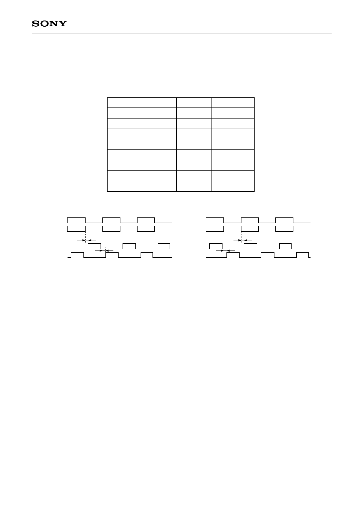
CXD3511Q
(3) DCKFINV and DCKFIX (sub address: 002h)
This setting switches the DCK1, DCK1X, DCK2 and DCK2X output phases relative to HCK1 and HCK2. The
phase changes as follows according to the combination of linked/not linked with right/left inversion control
signal RGT.
HCK1
HCK2
DCK1
DCK2
DCKFIX
0
0
0
0
1
1
1
1
A
DCKFINV
0
0
1
1
0
0
1
1
RGT
0
1
0
1
0
1
0
1
HCK1
HCK2
DCK1
DCK2
Output phase
A
B
B
A
B
B
A
A
B
(4) DCKOE (sub address: 02Dh)
This sets the output limit of DCK1 and DCK2 pulses.
Setting value: 1 = DCK1 and DCK2 pulses are output, 0 = Output is fixed to "0"
(5) DCKXOE (sub address: 02Dh)
This sets the output limit of DCK1X and DCK2X pulses.
Setting value: 1 = DCK1X and DCK2X pulses are output, 0 = Output is fixed to "0"
– 56 –
Page 57
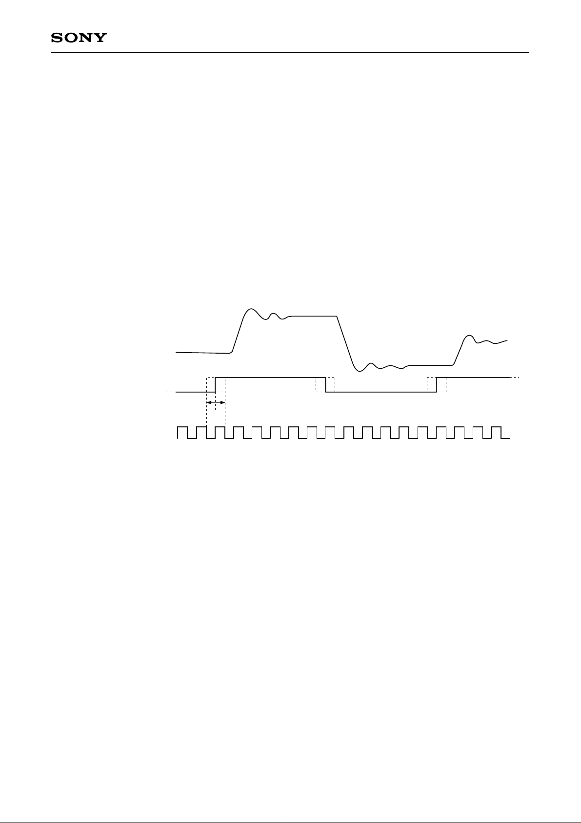
CXD3511Q
(k) LCD panel sample-and-hold position setting
SHP[5:0] (sub address: 014h)
This sets the horizontal transfer start pulse and clock pulse phases relative to the video signal to the LCD
panel. The phase can be set in 64 positions with 6 bits. Incrementing SHP by +1 shifts the HST, PST, HCK1,
HCK2, DCK1, DCK1X, DCK2 and DCK2X pulses forward by 1 dot (half the internal clock period). The LCD
panel sample-and-hold position can be set by shifting the above pulse phases forward or backward relative to
the video signal. At this time, the phases between the HST, PST, HCK1, HCK2, DCK1, DCK1X, DCK2 and
DCK2X pulses does not change. The figure below shows an example of HCK1 during 12-dot simultaneous
sampling.
This setting eliminates the need to set the sample-and-hold position with a Sony sample-and-hold driver IC
(CXA3512R, CXA3562R), and makes it possible to adjust the phases of the video signal to the LCD panel and
the horizontal transfer clock without changing the position of the video signal on the screen.
Video signal to LCD panel
HCK1
Internal CLK
SHP decreasedSHP increased
– 57 –
Page 58
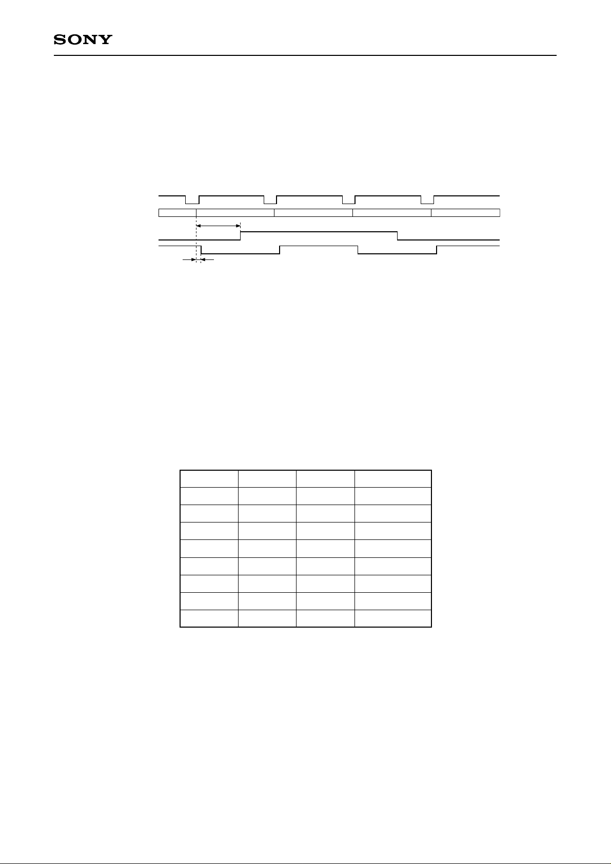
CXD3511Q
(l) VST and VCK pulse settings
(1) VST1P[11:2] and VST2P[11:2] (sub addresses: 026h to 027h)
These set the VSTL and VSTR pulse rise and f all positions within 1H in 10 bits. The position can be set in 4-dot
units using the internal HP counter "0" position as the reference. Set the "(Tvstp – 4)/4" value.
See the FRVC1LNK, RGVLNK and RGT settings hereafter to determine which of the VST1P or VST2P
settings is reflected to VSTL or VSTR.
HDIN
HP counter
VST
VCK
0
Tvstp
Tvckp
(2) VCK1P[10:1] and VCK2P[10:1] (sub addresses: 024h to 025h)
These set the VCKL, VCKR, FRP and XFRP inversion positions within 1H in 10 bits. The inversion positions
can be set in 2-dot units using the internal HP counter "0" position as the reference. Set the "(Tvckp – 2)/2"
value.
See the FRVC1LNK, RGVLNK and RGT settings hereafter to determine which of the VCK1P, VCK2P or FRPP
settings is reflected to VCKL or VCKR.
(3) VSTFIX and VCKFIX (sub address: 002h), VSTPOL and VCKPOL (sub address: 001h)
These set the VST and VCK pulse output polarities. The VSTL and VSTR pulse polarities and the VCKL and
VCKR pulse polarities relative to the VSTL and VSTR pulses change as follows according to the combination
of linked/not linked with control signal DWN.
∗∗∗
FIX
0
0
0
0
1
1
1
1
∗∗∗
POL
0
0
1
1
0
0
1
1
DWN
0
1
0
1
0
1
0
1
Output polarity
Positive
Negative
Negative
Positive
Negative
Negative
Positive
Positive
∗∗∗
: VST or VCK
(4) V1OE (sub address: 02Dh)
This sets the output limit of VSTL, VCKL and ENBL pulses.
Setting value: 1 = VSTL, VCKL and ENBL pulses are output, 0 = Output is fixed to "0"
(5) V2OE (sub address: 02Dh)
This sets the output limit of VSTR, VCKR and ENBR pulses.
Setting value: 1 = VSTR, VCKR and ENBR pulses are output, 0 = Output is fixed to "0"
– 58 –
Page 59

CXD3511Q
(m) FRP and XFRP pulse settings
(1) FRPM[1:0] (sub address: 002h)
This sets the period for switching the LCD AC conversion signal FRP pulse. 1F/1H, 2F/1H, 1F and 2F inversion
can be set as shown in the figure below. Normally use FRP1, 0: 11.
1H
FRP1, 0: 11
(1F/1H inversion)
FRP1, 0: 01
(2F/1H inversion)
FRP1, 0: 10
(1F inversion)
FRP1, 0: 00
(2F inversion)
1F
(2) FRPP[10:1] (sub address: 00Fh)
This sets the FRP and XFRP inversion positions within 1H in 10 bits. The inversion positions can be set in
2-dot units using the internal HP counter "0" position as the reference. Set the "(FRP inversion position –
HP counter "0" position – 2)/2" value.
XFRP is output as the polarity inverted FRP pulse.
(3) FRPOE and XFRPOE (sub address: 02Ch)
These set the FRP and XFRP pulse output limits, respectively.
Setting value: 1 = Pulse is output, 0 = Output is fixed to "0"
– 59 –
Page 60

CXD3511Q
(n) VCK and FRP transition point shared setting and V block pulse right/left inversion link setting
FRVC1LNK and RGVLNK (sub address: 003h)
These set the VCKL and VCKR transition points
Setting value: 1 = FRP and VCK transition points are shared,
0 = FRP and VCK transition points are independent
When FRVC1LNK = 1, the VCK inversion timing is forcibly synchronized with the FRP inversion timing. At this
time, which of VCKL or VCKR is linked with the FRP transition point is as follows.
When FRVC1LNK = 0, the VCKL and VCKR transition points are determined by VCK1P[10:1] or VCK2P[10:1]
according to the RGT setting. When RGVLNK = 1, the V block pulses, VSTL, VCKL and ENBL are switched
with VSTR, VCKR and ENBR, respectively, linked with right/left inversion control signal RGT. When RGVLNK =
0, the V block pulses are fixed regardless of the RGT setting. See the following page for a detailed description.
FRVC1LNK
0
0
0
0
1
1
1
1
VCKL
A
VCKR
FRP
VCKL
B
VCKR
FRP
RGVLNK
0
0
1
1
0
0
1
1
VCK2P
VCK2P
VCK1P
FRPP
VCK1P
FRPP
RGT
0
1
0
1
0
1
0
1
Output waveform
A
A
B
A
C
C
D
C
VCKL
C
VCKR
FRP
VCKL
VCKRD
FRP
VCK2P
FRPP
VCK2P
FRPP
– 60 –
Page 61
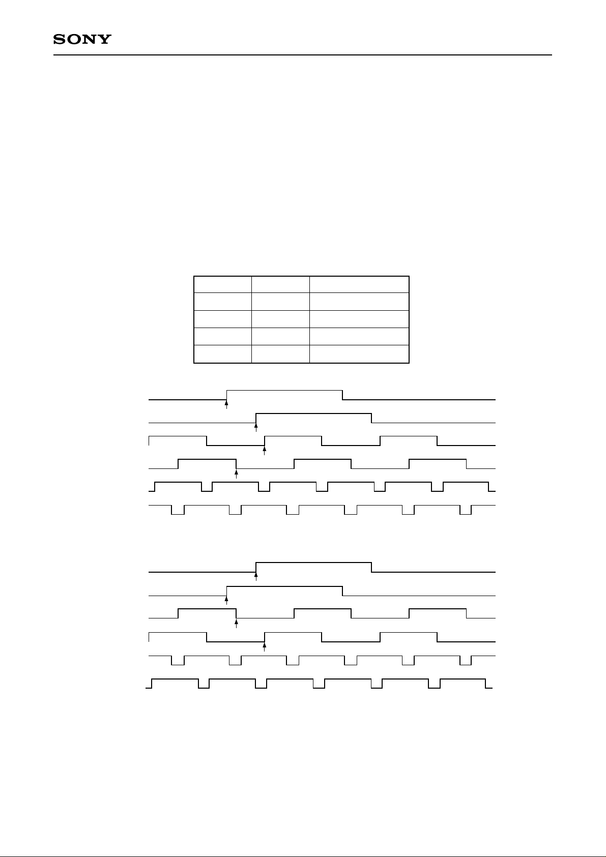
CXD3511Q
(o) V scanner pulse scan direction link setting
RGVLNK (sub address: 003h)
This sets whether to link the V block pulses, VSTL, VSTR, VCKL, VCKR, ENBL and ENBR with the right/left
inversion control signal RGT.
Setting value: 1 = Linked with RGT, 0 = Independent of RGT
When RGVLNK = 1, rise and fall positions of VSTL and VSTR, ENBL and ENBR pulses and inversion position
of VCKL and VCKR pulses are changed respectively by linking with RGT. When RGVLNK = 0, VSTL, VCKL
and ENBL are set by VST1P, VCK1P, ENB1U and ENB1D, respectively, and VSTR, VCKR and ENBR are set
by VST2P, VCK2P, ENB2U and ENB2D, respectively, independent of the RGT setting.
RGVLNK
0
0
1
1
VSTL
VST1P
VSTR
VCKL
A
VCKR
ENBL
ENBR
VSTL
VSTR
VST1P
VCKL
B
VCKR
ENBL
VCK2P
VCK2P
RGT
0
1
0
1
VST2P
VCK1P
ENB1UENB1D
VST2P
VCK1P
Output waveform
A
A
B
A
ENB2UENB2D
ENB2UENB2D
ENBR
ENB1UENB1D
– 61 –
Page 62
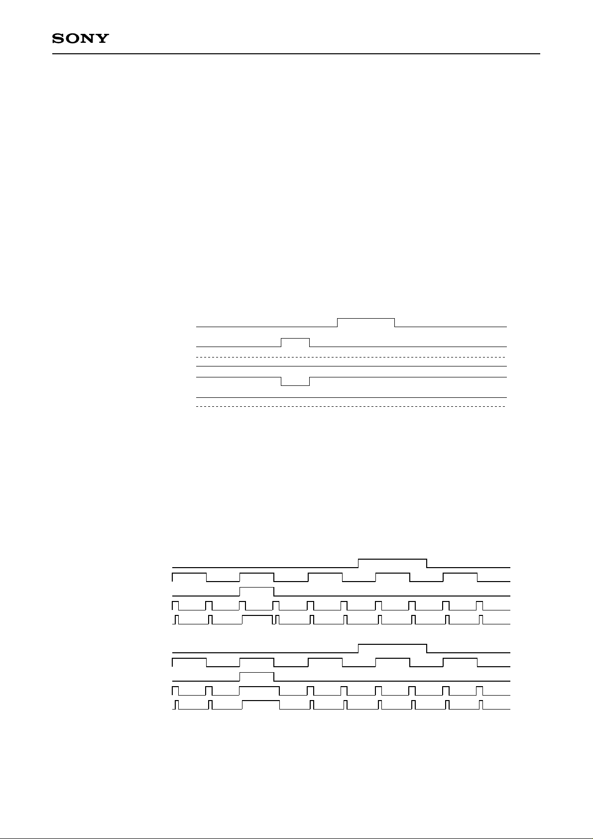
(p) BLK pulse settings
(1) BLKON (sub address: 001h)
This sets the black frame write pulse BLK ON/OFF.
Setting value: 1 = Pulse is output, 0 = DC is output
When BLKON = 1, BLK is output as a single pulse in 1V.
(2) BLKPOL (sub address: 001h)
This sets the black frame write pulse BLK polarity.
Setting value: 1 = Positive polarity, 0 = Negative polarity
Set BLKPOL = 1 for a Sony SVGA panel, and BLKPOL = 0 for an XGA panel.
VST
CXD3511Q
BLKON: 1, BLKPOL: 1
BLKON: 0, BLKPOL: 1
BLKON: 1, BLKPOL: 0
BLKON: 0, BLKPOL: 0
BLK
BLK
BLK
BLK
(3) SLXBLK (sub address: 003h)
This sets the precharge waveform top/bottom black frame display mode.
Setting value: 1 = XGA type, 0 = Other than XGA type
Set SLXBLK = 1 only when using top/bottom black frame display mode on a Sony XGA type LCD panel. Set
SLXBLK = 0 in all other cases.
VST
VCK
BLKSLXBLK: 0
PRG
PCG
VST
VCK
BLKSLXBLK: 1
PRG
PCG
– 62 –
Page 63

CXD3511Q
(4) BLKU[10:1] and BLKD[10:1] (sub addresses: 02Ah to 02Bh)
These set the BLK pulse rise and fall positions within 1H in 10 bits. The positions can be set in 2-dot units
using the internal HP counter "0" position as the reference. Set the "(BLK rise/fall position – HP counter "0"
position – 2)/2" value.
(5) BLKOE (sub address: 02Dh)
This is the BLK pulse output limit setting.
Setting value: 1 = Pulse is output, 0 = Output is fixed to "0"
– 63 –
Page 64
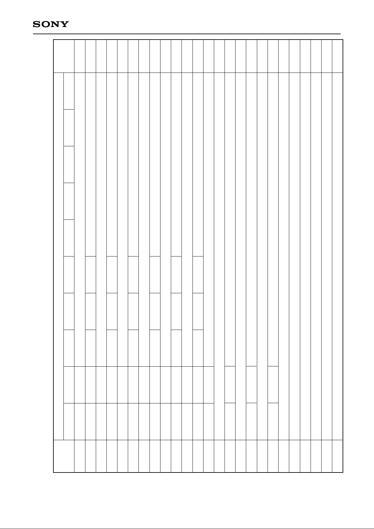
Initial value
CXD3511Q
000h
000h
000h
000h
000h
000h
000h
000h
000h
000h
000h
000h
000h
000h
000h
000h
000h
000h
000h
000h
000h
000h
000h
000h
000h
PDAT0
Data
R1_PRE_BRT[4:0]
R1_PRE_GAIN[7:0]
—
—
—
R2_PRE_BRT[4:0]
R2_PRE_GAIN[7:0]
—
—
—
G1_PRE_BRT[4:0]
G1_PRE_GAIN[7:0]
—
—
—
G2_PRE_BRT[4:0]
G2_PRE_GAIN[7:0]
—
—
—
B1_PRE_BRT[4:0]
B1_PRE_GAIN[7:0]
—
—
—
B2_PRE_BRT[4:0]
B2_PRE_GAIN[7:0]
GAM_ON
GAM_SEL
MUTE1_ON
USER_GAIN[7:0]
R_SUB_GAIN[7:0]
USER_BRT[9:0]
R_SUB_BRT[9:0]
G_SUB_GAIN[7:0]
B_SUB_GAIN[7:0]
G_SUB_BRT[9:0]
B_SUB_BRT[9:0]
R_MUTE1[9:0]
B_MUTE1[9:0]
G_MUTE1[9:0]
R_OSD_DAT1[9:0]
R_OSD_DAT2[9:0]
5-2. DSD1 Block (Main Address: 001h)
The DSD1 block data format is as follows.
PDAT8 PDAT7 PDAT6 PDAT5 PDAT4 PDAT3 PDAT2 PDAT1
R_DAT_SW
—
PDAT9
000h
Sub address
—
—
001h
—
—
002h
—
—
003h
G_DAT_SW
—
004h
—
—
005h
—
—
006h
—
—
007h
B_DAT_SW
—
008h
—
—
—
—
009h
00Ah
– 64 –
—
—
00Bh
USER_BRT[10]
—
00Ch
00Dh
R_SUB_BRT[10]
—
00Eh
00Fh
G_SUB_BRT[10]
—
010h
011h
B_SUB_BRT[10]
—
012h
013h
014h
015h
016h
017h
018h
Page 65
Initial value
PDAT0
000h
000h
000h
000h
000h
000h
000h
000h
000h
000h
000h
000h
000h
000h
000h
000h
000h
000h
000h
000h
000h
000h
000h
000h
CXD3511Q
000h
000h
000h
—: Don't care
Data
PDAT8 PDAT7 PDAT6 PDAT5 PDAT4 PDAT3 PDAT2 PDAT1
R_OSD_DAT3[9:0]
R_OSD_DAT4[9:0]
G_OSD_DAT1[9:0]
G_OSD_DAT2[9:0]
G_OSD_DAT3[9:0]
G_OSD_DAT4[9:0]
B_OSD_DAT1[9:0]
B_OSD_DAT2[9:0]
B_OSD_DAT3[9:0]
B_OSD_DAT4[9:0]
R_MUTE2[9:0]
B_MUTE2[9:0]
G_MUTE2[9:0]
L_LIM_DAT[9:0]
R1_POST_BRT[6:0]
R1_POST_GAIN[7:0]
H_LIM_DAT[9:0]
MUTE2_ON
R2_POST_GAIN[7:0]
—
—
—
R2_POST_BRT[6:0]
—
—
G1_POST_BRT[6:0]
G1_POST_GAIN[7:0]
—
G2_POST_GAIN[7:0]
—
—
—
G2_POST_BRT[6:0]
—
—
B1_POST_BRT[6:0]
B1_POST_GAIN[7:0]
—
B2_POST_GAIN[7:0]
—
—
—
B2_POST_BRT[6:0]
—
—
PDAT9
019h
Sub address
01Ah
01Bh
01Ch
01Dh
01Eh
01Fh
020h
021h
022h
023h
024h
025h
– 65 –
026h
027h
—
028h
—
029h
—
02Ah
—
02Bh
—
02Ch
—
02Dh
—
02Eh
—
02Fh
—
030h
—
031h
—
032h
—
033h
Page 66

CXD3511Q
The detailed setting contents are described below.
(a) R_DAT_SW, G_DAT_SW and B_DAT_SW (sub addresses: 000h, 004h and 008h)
These select the data path switch block data path.
Setting value: 1 = Data path is switched, 0 = Data path is not switched
(b) R1_PRE_GAIN[7:0], R2_PRE_GAIN[7:0], G1_PRE_GAIN[7:0], G2_PRE_GAIN[7:0],
B1_PRE_GAIN[7:0] and B2_PRE_GAIN[7:0] (sub addresses: 000h, 002h, 004h, 006h, 008h and
00Ah)
These set the pre gain block arithmetic coefficients in 8 bits.
(c) R1_PRE_BRT[4:0], R2_PRE_BRT[4:0], G1_PRE_BRT[4:0], G2_PRE_BRT[4:0], B1_PRE_BRT[4:0]
and B2_PRE_BRT[4:0] (sub addresses: 001h, 003h, 005h, 007h, 009h and 00Bh)
These set the pre bright block arithmetic coefficients in 5 bits with code.
(d) USER_GAIN[7:0] (sub address: 00Ch)
This sets the user gain block arithmetic coefficients in 8 bits.
(e) USER_BRT[10:0] (sub addresses: 00Ch and 00Dh)
This sets the user bright block arithmetic coefficients in 11 bits with code.
(f) R_SUB_GAIN[7:0], G_SUB_GAIN[7:0] and B_SUB_GAIN[7:0] (sub addresses: 00Eh, 010h and
012h)
These set the R, G and B sub gain block arithmetic coefficients in 8 bits.
(g) R_SUB_BRT[10:0], G_SUB_BRT[10:0] and B_SUB_BRT[10:0] (sub addresses: 00Eh to 013h)
These set the R, G and B sub bright block arithmetic coefficients in 11 bits with code.
(h) MUTE1_ON (sub address: 00Bh)
This selects mute 1 block processing ON/OFF.
Setting value: 1 = Mute processing ON, 0 = OFF
(i) R_MUTE1[9:0], G_MUTE1[9:0] and B_MUTE1[9:0] (sub addresses: 014h to 016h)
These set the mute 1 block data in 10 bits.
– 66 –
Page 67

CXD3511Q
(j) R_OSD_DAT1 to 4[9:0], G_OSD_DAT1 to 4[9:0] and B_OSD_DAT1 to 4[9:0] (sub addresses: 014h
to 022h)
These set the OSD block decode data in 10 bits.
(k) GAM_SEL (sub address: 00Bh)
This selects the gamma block data path.
Setting value: 1 = Path passing through the RAM, 0 = Path not passing through the RAM
(l) GAM_ON (sub address: 00Bh)
This sets the gamma block RAM operating mode.
Setting value: 1 = Normal operation, 0 = Standby mode
Note that in standby mode, data cannot be written to or read from the RAM. Also, previously set data is held
even when the RAM is set to standby mode.
(m) L_LIM_DAT[9:0] and H_LIM_DAT[9:0] (sub addresses: 026h and 027h)
This sets the limiter block limit value data in 10 bits.
Be sure to maintain the relationship L_LIM_DAT < H_LIM_DAT. Note that when both coefficients are set to
000h, limiter processing is not performed.
(n) MUTE2_ON (sub address: 028h)
This selects mute 2 block processing ON/OFF.
Setting value: 1 = Mute processing ON, 0 = OFF
(o) R_MUTE2[9:0], G_MUTE2[9:0] and B_MUTE2[9:0] (sub addresses: 023h to 025h)
These set the mute 2 block data in 10 bits.
(p) R1_POST_GAIN[7:0], R2_POST_GAIN[7:0], G1_POST_GAIN[7:0], G2_POST_GAIN[7:0],
B1_POST_GAIN[7:0] and B2_POST_GAIN[7:0] (sub addresses: 028h, 02Ah, 02Ch, 02Eh, 030h and
032h)
These set the post gain block arithmetic coefficients in 8 bits.
(q) R1_POST_BRT[6:0], R2_POST_BRT[6:0], G1_POST_BRT[6:0], G2_POST_BRT[6:0],
B1_POST_BRT[6:0] and B2_POST_BRT[6:0] (sub addresses: 029h, 02Bh, 02Dh, 02Fh, 031h and
033h)
These set the post bright block arithmetic coefficients in 7 bits with code.
– 67 –
Page 68
Initial value
PDAT0
000h
000h
000h
000h
000h
000h
000h
CSC_R_RGT
000h
000h
000h
000h
000h
000h
DLY_R_RGT
000h
000h
000h
000h
000h
000h
000h
CXD3511Q
000h
000h
000h
000h
Data
FRM_H1[9:0]
FRM_DAT[9:0]
FRM_V1[9:0]
FRM_H2[9:0]
FRM_V2[9:0]
CSC_G_RGT
CSC_B_RGT
FRM_H1[11:10] FRM_H2[11:10]
CSC_DWN
FRM_V2[10]
CSC_HP[10:1]
CCS_H_MODE[1:0]
FRM_V1[10]
FRM_ON
CSC_VP[9:0]
CSC_VNUM[9:0]
CSC_HNUM[9:0]
DLY_G_RGT
DLY_B_RGT
R_OFFSET1[4:0]
R_OFFSET3[4:0]
DLY_DWN
DLY_ON
RGT_SEL_ON
R_OFFSET5[4:0]
R_OFFSET7[4:0]
R_OFFSET9[4:0]
R_OFFSET11[4:0]
R_OFFSET13[4:0]
R_OFFSET15[4:0]
R_OFFSET17[4:0]
R_OFFSET19[4:0]
R_OFFSET21[4:0]
R_OFFSET23[4:0]
5-3. DSD2 Block (Main Address: 002h)
The DSD2 block data format is as follows.
PDAT8 PDAT7 PDAT6 PDAT5 PDAT4 PDAT3 PDAT2 PDAT1
PDAT9
000h
Sub address
001h
002h
003h
CSC_XH_ON
—
—
004h
005h
CSC_V_MODE[1:0]
CSC_G_MODE
CSC_ON
006h
007h
008h
009h
– 68 –
OFFSET_MODE[1:0]
R_OFFSET2[4:0]
R_OFFSET4[4:0]
OFFSET_ON
—
00Ah
00Bh
00Ch
00Dh
R_OFFSET6[4:0]
R_OFFSET8[4:0]
R_OFFSET10[4:0]
R_OFFSET12[4:0]
010h
00Eh
00Fh
011h
R_OFFSET14[4:0]
R_OFFSET16[4:0]
R_OFFSET18[4:0]
R_OFFSET20[4:0]
012h
013h
014h
015h
R_OFFSET22[4:0]
R_OFFSET24[4:0]
016h
017h
Page 69
000h
Initial value
PDAT0
G_OFFSET1[4:0]
000h
000h
000h
000h
G_OFFSET3[4:0]
G_OFFSET5[4:0]
G_OFFSET7[4:0]
G_OFFSET9[4:0]
000h
000h
000h
000h
G_OFFSET11[4:0]
G_OFFSET13[4:0]
G_OFFSET15[4:0]
G_OFFSET17[4:0]
000h
000h
000h
000h
G_OFFSET19[4:0]
G_OFFSET21[4:0]
B_OFFSET1[4:0]
G_OFFSET23[4:0]
000h
000h
000h
000h
B_OFFSET3[4:0]
B_OFFSET5[4:0]
B_OFFSET7[4:0]
B_OFFSET9[4:0]
000h
000h
000h
000h
B_OFFSET11[4:0]
B_OFFSET13[4:0]
B_OFFSET15[4:0]
B_OFFSET17[4:0]
CXD3511Q
000h
000h
000h
—: Don't care
B_OFFSET19[4:0]
B_OFFSET21[4:0]
B_OFFSET23[4:0]
Data
G_OFFSET2[4:0]
G_OFFSET4[4:0]
PDAT8 PDAT7 PDAT6 PDAT5 PDAT4 PDAT3 PDAT2 PDAT1
PDAT9
G_OFFSET6[4:0]
G_OFFSET8[4:0]
G_OFFSET10[4:0]
G_OFFSET12[4:0]
G_OFFSET14[4:0]
G_OFFSET16[4:0]
G_OFFSET18[4:0]
G_OFFSET20[4:0]
B_OFFSET2[4:0]
G_OFFSET22[4:0]
G_OFFSET24[4:0]
B_OFFSET4[4:0]
B_OFFSET6[4:0]
B_OFFSET8[4:0]
B_OFFSET10[4:0]
B_OFFSET12[4:0]
B_OFFSET14[4:0]
B_OFFSET16[4:0]
B_OFFSET18[4:0]
B_OFFSET20[4:0]
B_OFFSET22[4:0]
B_OFFSET24[4:0]
018h
Sub address
019h
01Ah
01Bh
01Ch
01Dh
01Eh
01Fh
020h
021h
022h
023h
024h
– 69 –
025h
026h
027h
028h
029h
02Ah
02Bh
02Ch
02Dh
02Eh
02Fh
Page 70
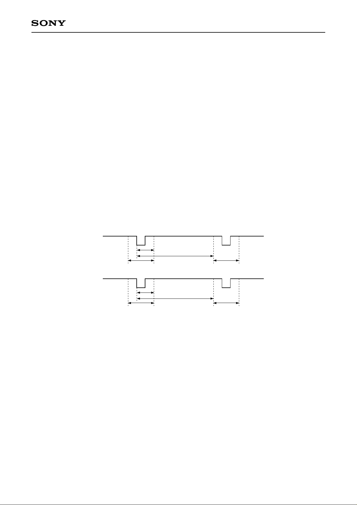
CXD3511Q
The detailed setting contents are described below.
(a) FRM_DAT[9:0] (sub address: 000h)
This sets the black frame level for the black frame block in 10 bits.
(b) FRM_ON (sub address: 005h)
This sets black frame display ON/OFF for the black frame block.
Setting value: 1 = ON, 0 = OFF
(c) FRM_H1[11:0] and FRM_H2[11:0] (sub addresses: 001h, 002h and 005h)
These set the horizontal black frame display range for the black frame block in 12 bits. The range can be set in
1-dot units using the front edge of the HDIN input as the reference. Set the "display range" value.
(d) FRM_V1[10:0] and FRM_V2[10:0] (sub addresses: 003h to 005h)
These set the vertical black frame display range for the black frame block in 11 bits. The range can be set in
1-line units using the front edge of the VDIN input as the reference. Set the "display range – 3" value.
HDIN
FRM_H1
FRM_H2
Black frame display range Black frame display range
VDIN
FRM_V1
FRM_V2
Black frame display range Black frame display range
(e) CSC_ON (sub address: 006h)
This sets color shading correction processing ON/OFF for the color shading correction block.
Setting value: 1 = ON, 0 = OFF
(f) CSC_H_MODE[1:0] (sub address: 006h)
This sets the horizontal correction point interval for the color shading correction of the color shading correction
block.
Setting value: 0h = 32-dot interval, 1h = 64-dot interval, 2h = 128-dot interval
– 70 –
Page 71

CXD3511Q
(g) CSC_V_MODE[1:0] (sub address: 006h)
This sets the vertical correction point interval for the color shading correction of the color shading correction
block.
Setting value: 0h = 32-line interval, 1h = 64-line interval, 2h = 128-line interval
(h) CSC_G_MODE (sub address: 006h)
This sets the scale correction ON/OFF for the color shading correction of the color shading correction block.
Setting value: 1 = Scale correction ON, 0 = OFF
(i) CSC_R_RGT, CSC_G_RGT and CSC_B_RGT (sub address: 006h)
These set the right/left inversion for the color shading correction block.
Setting value: 1 = Reflects the TG block RGT setting, 0 = Reflects the inverse of TG block RGT setting
(j) CSC_DWN (sub address: 006h)
This sets the up/down inversion for the color shading correction block.
Setting value: 1 = Reflects the TG block DWN setting, 0 = Reflects the inverse of TG block DWN setting
(k) CSC_HP[10:1] (sub address: 007h)
This sets the horizontal correction start position for the color shading correction block in 10 bits. The position
can be set in 2-dot units using the front edge of the HDIN input as the reference. Set the "(correction star t
position – 4)/2" value.
(l) CSC_VP[9:0] (sub address: 008h)
This sets the vertical correction start position for the color shading correction block in 10 bits. The position can
be set in 1-line units using the front edge of the VDIN input as the reference. Set the "correction start position
– 3" value.
(m) CSC_HNUM[9:0] and CSC_VNUM[9:0] (sub addresses: 009h and 00Ah)
These set the number of horizontal and vertical correction points for the color shading correction b l o ck in 10 bits.
Set the "(number of correction points – 1)" value. The size of the RAM for setting the correction data is 520
words, so set the number of correction points as follows.
Number of horizontal correction points × Number of vertical correction points ≤ 520
(n) CSC_XH_ON (sub address: 005h)
This sets the cross hatch display ON/OFF for the color shading correction block.
Setting value: 1 = Displayed, 0 = Not displayed
– 71 –
Page 72
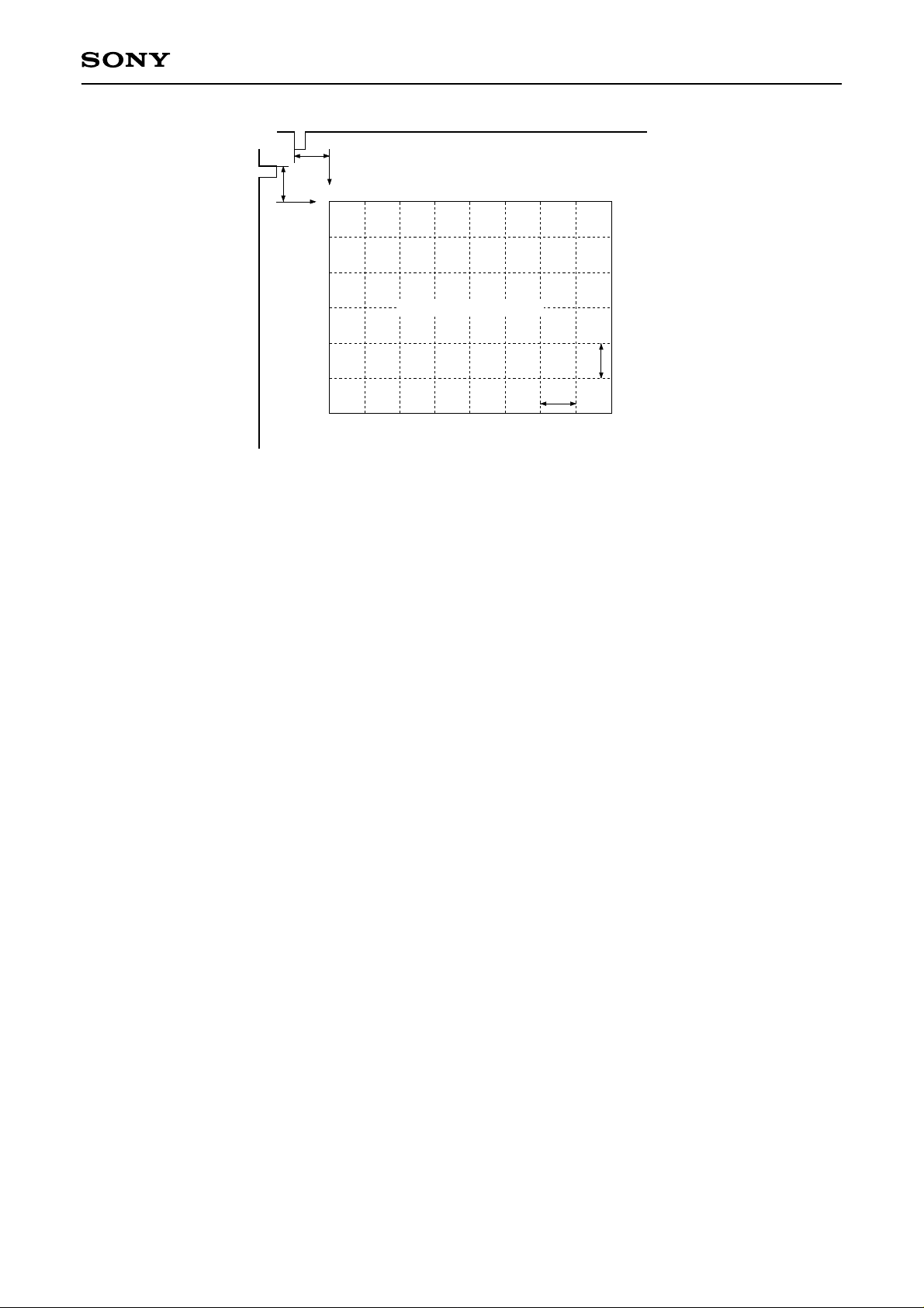
HDIN
CXD3511Q
VDIN
Correction start position
CSC_HP
12
1
2
CSC_VP
3
4
Correction start position
5
6
7
CSC_VNUM
Number of correction points
3456789
Color shading correction range
Correction interval
CSC_H_MODE
CSC_HNUM
Number of correction points
CSC_V_MODE
Correction interval
(o) RGT_SEL_ON, DLY_ON, DLY_DWN, DLY_R_RGT, DLY_G_RGT and DLY_B_RGT (sub address: 00Bh)
These are the selectable delay line block settings.
RGT_SEL_ON: This sets ON/OFF for port switching linked with left/right inversion.
Setting value: 1 = ON, 0 = OFF
DLY_ON: This sets the dot/line inverted dr ive support ON/OFF.
Setting value: 1 = ON, 0 = OFF
DLY_DWN: This sets the up/down inversion for the selectable delay line block.
Setting value: 1 = Reflects the TG block DWN setting,
0 = Reflects the inverse of the TG block DWN setting
DLY_R_RGT, DLY_G_RGT and DLY_B_RGT: These set the right/left inversion for the selectable delay line block.
Setting value: 1 = Reflects the TG block RGT setting,
0 = Reflects the inverse of the TG block RGT setting
The initial value is 0h for all settings.
(p) OFFSET_ON (sub address: 00Bh)
This sets the offset processing ON/OFF for the cycle offset block.
Setting value: 1 = ON, 0 = OFF
(q) OFFSET_MODE[1:0] (sub address: 00Bh)
This sets the offset cycle for the cycle offset block.
Setting value: 0h = 6-dot cycle, 1h = 12-dot cycle, 2h = 24-dot cycle
(r) R_OFFSET1 to 24, G_OFFSET1 to 24 and B_OFFSET1 to 24 (sub addresses: 00Ch to 02Fh)
These set the offset data for the cycle offset block in 5 bits with code.
– 72 –
Page 73

CXD3511Q
5-4. Gamma Block RAM (Main Address: 003h to 005h)
In the gamma block, the gamma correction data is set in a 10-bit × 1024-word RAM. Here, the set sub address
directly becomes the RAM write address. Thereafter, the RAM write address is automatically incremented by
+1. Following the main address, designate the RAM write star t address in the sub address with 10 bits, then
set the gamma correction data in PDAT[9:0] with 10 bits. Note that GAM_ON of the DSD1 block should be set
to "1" before setting data in the RAM.
5-5. Color Shading Correction Block RAM (Main Address: 006h to 014h)
In the color shading correction block, the color shading correction data is set in an 8-bit × 520-word RAM.
Here, the set sub address directly becomes the RAM write address. Thereafter, the RAM write address is
automatically incremented by +1. Following the main address, designate the RAM write start address in the
sub address with 10 bits, then set the color shading correction data in PDAT[7:0] with 8 bits. Note that
CSC_ON and CSC_G_MODE of the DSD2 block should be set to "1" before setting data in the RAM.
– 73 –
Page 74

Initial value
CXD3511Q
000h
000h
000h
000h
000h
000h
000h
000h
000h
000h
000h
000h
000h
000h
000h
000h
000h
000h
—: Don't care
PDAT0
PG_VWSTP[11]
PDAT1
PG_PAT[2:0]
PG_VWST[11]
PG_VSTP[10]
Data
PG_B_SEL
PDAT4 PDAT3 PDAT2
PG_G_SEL
PDAT5
PG_R_SEL
PG_B_ON
PG_G_ON
PDAT8 PDAT7 PDAT6
PG_R_ON
PG_VST[10]
PG_HWSTP[11]
PG_HST[10:1]
PG_HSTP[10:1]
PG_HWST[10:1]
PG_HWST[11]
PG_HSTP[11]
PG_HST[11]
PG_STAIR_SW
PG_VST[9:0]
PG_VSTP[9:0]
PG_HWSTP[10:1]
PG_VWST[9:0]
PG_SIG1R[9:0]
PG_SIG2R[9:0]
PG_VWSTP[9:0]
PG_WIDTH[9:0]
PG_STEP[9:1]
PG_SIG1G[9:0]
PG_SIG1B[9:0]
PG_SIG2G[9:0]
PG_SIG2B[9:0]
5-6. Pattern Generator Block (Main Address: 015h)
The pattern generator block data format is as follows.
PDAT9
PG_ON
000h
Sub address
PG_STRP_SW
001h
002h
003h
004h
005h
006h
007h
008h
– 74 –
009h
—
00Ah
00Bh
00Ch
00Dh
00Eh
00Fh
010h
011h
Page 75
The detailed setting contents are described below.
(a) PG_ON (sub address: 000h)
This sets the test signal output ON/OFF.
Setting value: 1 = Test pattern output mode enabled, 0 = Normal signal output
(b) PG_R (G, B)_ON (sub address: 000h)
These set the test signal level setting ON/OFF.
Setting value: 1 = Various settings enabled, 0 = Output fixed to "0"
(c) PG_R (G, B)_SEL (sub address: 000h)
These switch the pattern and non-pattern signal levels within the effective area.
Setting value: 1 = Pattern signal level is PG_SIG1R (G, B), 0 = Pattern signal level is PG_SIG2R (G, B)
(d) PG_PAT[2:0] (sub address: 000h)
CXD3511Q
This switches the display pattern within the window area.
Setting value: See the table below.
0
1
2
Vertical stripe/diagonal str ipe
3
4
5
6
Horizontal ramp/horizontal stair
7
Vertical ramp/vertical stair
Raster
Window
Horizontal stripe
Cross hatch
Dot
(e) PG_STRP_SW (sub address: 001h)
(Valid only when PG_PAT[2:0] = 2h)
This switches between vertical stripe and diagonal str ipe.
Setting value: 1 = Diagonal stripe, 0 = Vertical stripe
(f) PG_STAIR_SW (sub address: 001h)
(Valid only when PG_PAT[2:0] = 6h or 7h)
This switches between ramp and stair.
Setting value: 1 = Stair, 0 = Ramp
(g) PG_HST[11:1] (sub addresses: 001h and 002h)
PG_HSTP[11:1] (sub addresses: 001h and 003h)
These set the horizontal effective area in 11 bits. The area can be set in 2-dot units using the front edge of the
HDIN input as the reference. Set the "(set point – 50)/2" value.
– 75 –
Page 76
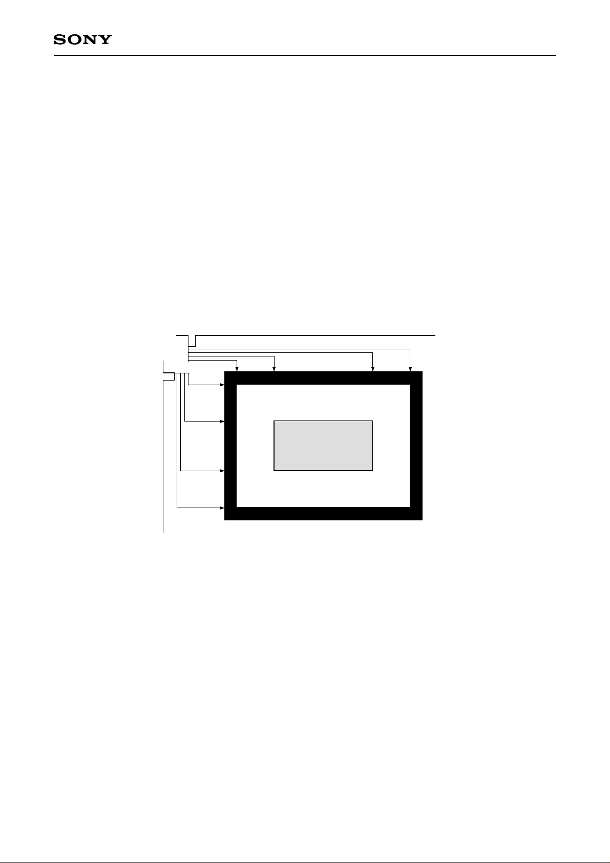
CXD3511Q
(h) PG_HWST[11:1] (sub addresses: 001h and 004h)
PG_HWSTP[11:1] (sub addresses: 001h and 005h)
These set the horizontal window area in 11 bits. The area can be set in 2-dot units using the front edge of the
HDIN input as the reference. Set the "(set point – 52)/2" value.
(i) PG_VST[10:0] (sub addresses: 001h and 006h)
PG_VSTP[10:0] (sub addresses: 001h and 007h)
These set the vertical effective area in 11 bits. The area can be set in 1-line units using the front edge of the
VDIN input as the reference. Set the "set point – 3" value.
(j) PG_VWST[10:0] (sub addresses: 001h and 008h)
PG_VWSTP[10:0] (sub addresses: 001h and 009h)
These set the vertical window area in 11 bits. The area can be set in 1-line units using the front edge of the
VDIN input as the reference. Set the "set point – 4" value.
HDIN
VDIN
PG_HST
PG_VST
PG_VWST
PG_VWSTP
PG_VSTP
PG_HWST PG_HSTPPG_HWSTP
Effective area
Window area
(k) PG_STEP[9:1] (sub address: 00Ah)
(Valid for PG_PAT[2:0] = 2h, 3h, 4h, and 5h)
This sets the vertical stripe, diagonal stripe, horizontal stripe, cross hatch and dot period in 9 bits. The period
can be set in 2-dot units. Set the "(period – 2)/2" value.
(l) PG_WIDTH[9:0] (sub address: 00Bh)
(Valid for PG_PAT[2:0] = 2h, 3h, 4h, and 5h)
This sets the vertical stripe, diagonal stripe, horizontal stripe, cross hatch and dot line width in 10 bits. The
width can be set in 1-dot units. Set the "width" value.
(m) PG_SIG1R (G, B)[9:0] and PG_SIG2R (G, B)[9:0] (sub addresses: 00Ch to 011h)
These set the output signal level inside and outside the pattern area within the effective area in 10 bits. The
level can be set with an accuracy of 1 bit.
– 76 –
Page 77

CXD3511Q
Notes on Handling
• The power supply and GND patterns have a large effect on undesired radiation on the substrate and
interference to analog circuits, etc. General precautions are as follows.
• Make the GND pattern as wide as possible. Using a multi-layer substrate and a solid ground is
recommended.
• Connect each power supply pin to GND via a ceramic chip capacitor of 0.1µF or more located as close
to each pin as possible.
• Do not use this IC under conditions other than the recommended operating conditions.
• Absolute maximum rating values should not be exceeded even momentarily. Exceeding ratings may damage
the device, leading to eventual breakdown.
• This IC has a MOS structure which is easily damaged by static electricity, so thorough measures should be
taken to prevent electrostatic discharge.
• Since this IC utilizes a MOS structure, it may latch up due to excessive noise or power surge greater than the
maximum rating of the I/O pins, interface with two power supplies of another circuit, or the order in which
power is supplied to circuits. Make a thorough study of measures against the possibility of latch up before
use.
• When the initialization of this IC is performed at power-on, system clear cancellation is performed after the
supply voltage is set in the range of the recommended operating conditions and stabilized. Keep in mind that
the internal circuit may not be initialized correctly if system clear cancellation is performed before the supply
voltage is set in the range of the recommended operating conditions.
• When designing the substrate, take sufficient care for the surrounding temperature and heat radiation, and
make sure the IC junction temperature does not exceed the maximum value.
• Be sure to make the number of dot clocks input to the CXD3511Q in 1H an even number. Note that if there is
an odd number of dot clocks, the internal phase compensation PLL will not operate properly.
• Be sure to make a thorough evaluation of any items not listed in this data sheet.
– 77 –
Page 78
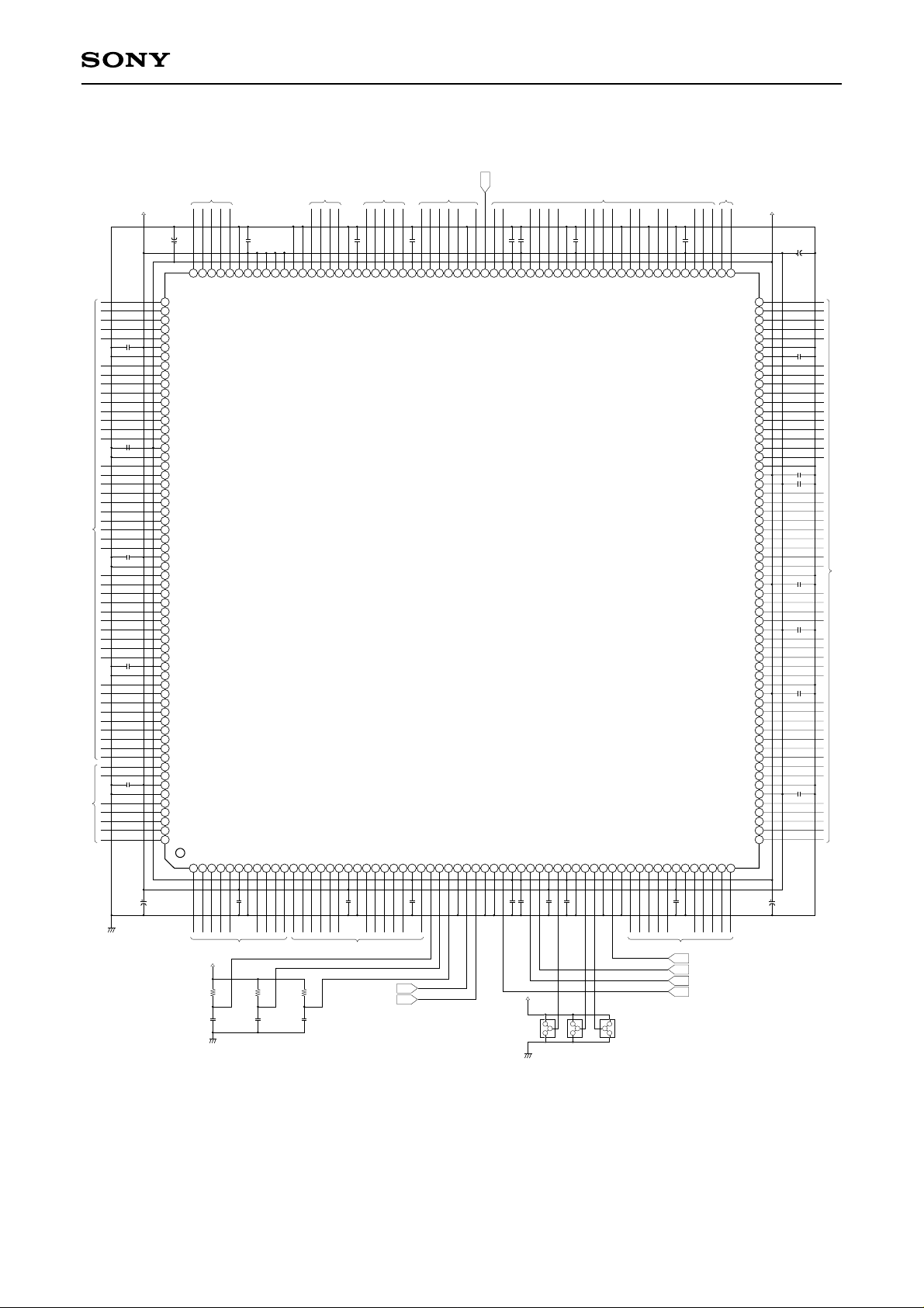
Application Circuit
+3.3V
From A/D converter Auxiliary pulse To S/H driver To LCD panel To LCD panel To D/A converter
10µ 0.1µ 0.1µ 0.1µ
CXD3511Q
CTRL
+2.5V
0.1µ 0.1µ 0.1µ
From A/D converterOSD input
165
164
TEST4
YM2
TEST3
YS2
TEST2
PCTL
TEST1
PCLK
166167168169170171172173174175176177178179180
SS
DD1
V
CLP
HD1
PO5
PO4
V
DD2VSS
PDAT9
PDAT8
PDAT7
PDAT6
V
DD1
FRP
PRG
V
SHST
XFRP
DENB
DD1
PDAT5
PDAT4
PDAT3
PDAT2
PDAT1
V
SS
V
PST
HD2
PO1
PO2
PO3
PCG
DWN
CTRL
PDAT0
XCLR1
XCLR2
XCLR3
VSSHDIN
VDIN
VSSVSSCLKC
SS
DD2
V
R1IN5
R1IN6
R2OSD0
G2OSD1
R1IN7
G2OSD0
DD2VSS
V
V
TEST6
B2OSD1
TEST5
B2OSD0
R1IN3
R1IN4
181
R1IN2
182
R1IN1
183
R1IN0
184
R2IN7
185
0.1µ
0.1µ
0.1µ
0.1µ
0.1µ
R2IN6
186
V
DD2
187
SS
V
188
R2IN5
189
R2IN4
190
R2IN3
191
R2IN2
192
R2IN1
193
R2IN0
194
G1IN7
195
G1IN6
196
G1IN5
197
V
DD1
198
SS
V
199
G1IN4
200
G1IN3
201
G1IN2
202
G1IN1
203
G1IN0
204
G2IN7
G2IN6
205
G2IN5
206
G2IN4
207
G2IN3
208
V
DD1
209
SS
V
210
G2IN2
211
G2IN1
212
G2IN0
213
B1IN7
214
B1IN6
215
B1IN5
216
B1IN4
217
B1IN3
218
B1IN2
219
B1IN1
220
V
DD1
221
SS
V
222
B1IN0
223
B2IN7
224
B2IN6
225
B2IN5
226
B2IN4
227
B2IN3
228
B2IN2
229
B2IN1
230
B2IN0
231
R1OSD1
232
R1OSD0
233
V
DD2
234
V
SS
235
G1OSD1
236
G1OSD0
237
B1OSD1
238
B1OSD0
239
YM1
240
YS1
R2OSD1
1 2 3 4 5 6 7 8 9 10 11 12 13 14 15 16 17 18 19 20 21 22 23 24 25 26 27 28 29 30 31 32 33 34 35 36 37 38 39 40
VSTL
DD1VDD2
V
DD1VDD1
V
VCKL
CLKP
ENBL
CLKN
141142143144145146147148149150151152153154155156157158159160161162
BLK
DD2
V
135136137138139140
134
133
132
SS
DD2
V
HST
V
XRGT
DD1VSS
CLKSEL1
V
CLKSEL2
41 42 43 44 53 54 55 56 57 58 59 60
131
SS
V
RGT
HCK1
DCK1
HCK2
PLLDIV
VSSCLKOUT
VSSB2OUT0
45 46 47 48 49 50 51 52
130
DCK1X
B2OUT1
129
SS
V
B2OUT2
DCK2X
B2OUT3
127128
DCK2
B2OUT4
SS
V
DD2VSS
V
126
125
124
123
122
121
DD2
V
VSTR
ENBR
VCKR
R2OUT9
R1OUT8
R1OUT7
R1OUT6
R1OUT5
R1OUT4
R1OUT3
V
SS
V
DD2
R1OUT2
R1OUT1
R1OUT0
R2OUT9
R2OUT8
R2OUT7
R2OUT6
R2OUT5
R2OUT4
R2OUT3
R2OUT2
V
SS
V
DD1
DD2
V
R2OUT1
R2OUT0
G1OUT9
G1OUT8
G1OUT7
G1OUT6
G1OUT5
G1OUT4
G1OUT3
V
SS
DD1
V
G1OUT2
G1OUT1
G1OUT0
G2OUT9
DD2
V
G2OUT8
G2OUT7
G2OUT6
G2OUT5
G2OUT4
V
SS
V
DD1
G2OUT3
G2OUT2
G2OUT1
G2OUT0
B1OUT9
B1OUT8
B1OUT7
B1OUT6
B1OUT5
V
SS
DD2
V
B1OUT4
B1OUT3
B1OUT2
B1OUT1
B1OUT0
B2OUT5
B2OUT6
B2OUT7
B2OUT8
B2OUT9
0.1µ
120
119
118
117
116
115
114
113
112
111
110
109
108
107
106
105
104
103
102
101
100
99
98
97
96
95
94
93
92
91
90
89
88
87
86
85
84
83
82
81
80
79
78
77
76
75
74
73
72
71
70
69
68
67
66
65
64
63
62
61
0.1µ
0.1µ
0.1µ
To D/A converter
0.1µ
0.1µ
0.1µ
163
10µ
10µ 10µ
0.1µ
GND
OSD input
+3.3V
10k
10k
10k
1µ
1µ
1µ
0.1µ 0.1µ 0.1µ 0.1µ 0.1µ 0.1µ
Parallel data input To D/A converter
HDIN1
VDIN1
+3.3V
CLKOUT
CLKN
CLKP
CLKC
GND
GND
CLKSEL1
Application circuits shown are typical examples illustrating the operation of the devices. Sony cannot assume responsibility for
any problems arising out of the use of these circuits or for any infringement of third party patent and other right due to same.
CLKSEL2
PLLDIV
– 78 –
Page 79
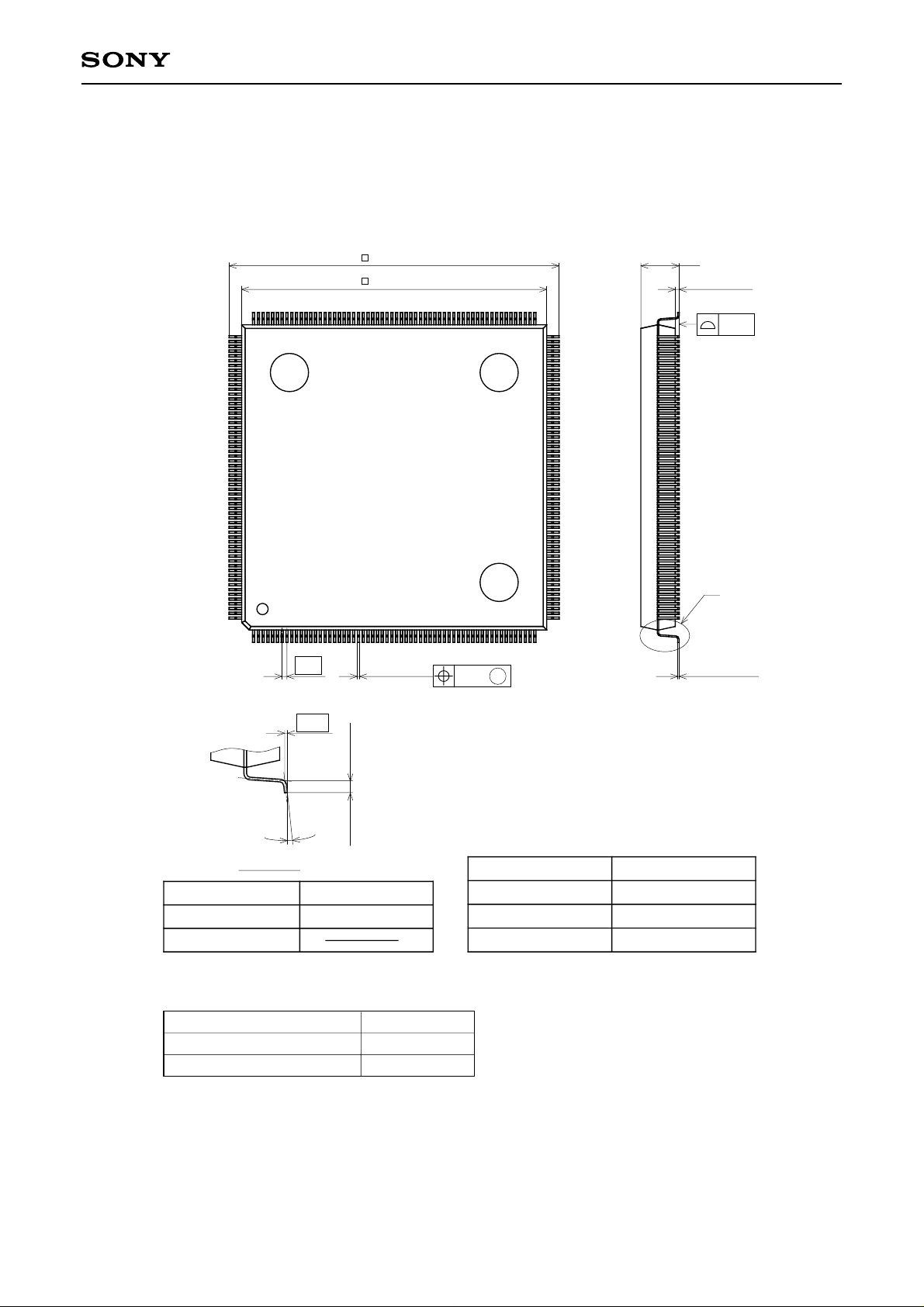
Package Outline Unit: mm
CXD3511Q
240PIN QFP (PLASTIC)
34.6 ± 0.2
32.0 ± 0.1
4.1 MAX
0.40 – 0.15
180 121
181
120
A
240
160
0.5
+ 0.05
0.22 – 0.03
0.08
M
61
0.145 – 0.03
+ 0.10
0.10
+ 0.05
0.25
0˚ to 8˚
0.45 MIN – 0.75 MAX
DETAIL A
SONY CODE
EIAJ CODE
JEDEC CODE
QFP-240P-L022
QFP240-P-3232
LEAD SPECIFICATIONS
ITEM
SPEC.
LEAD MATERIAL COPPER ALLOY
LEAD TREA TMENT Sn-Bi
PACKAGE STRUCTURE
PACKAGE MATERIAL
LEAD TREA TMENT
LEAD MATERIAL
PACKAGE MASS
EPOXY RESIN
SOLDER PLATING
COPPER ALLOY
7.6g
– 79 –
Sony Corporation
 Loading...