

Page 1
– 1 –
CXG1017N
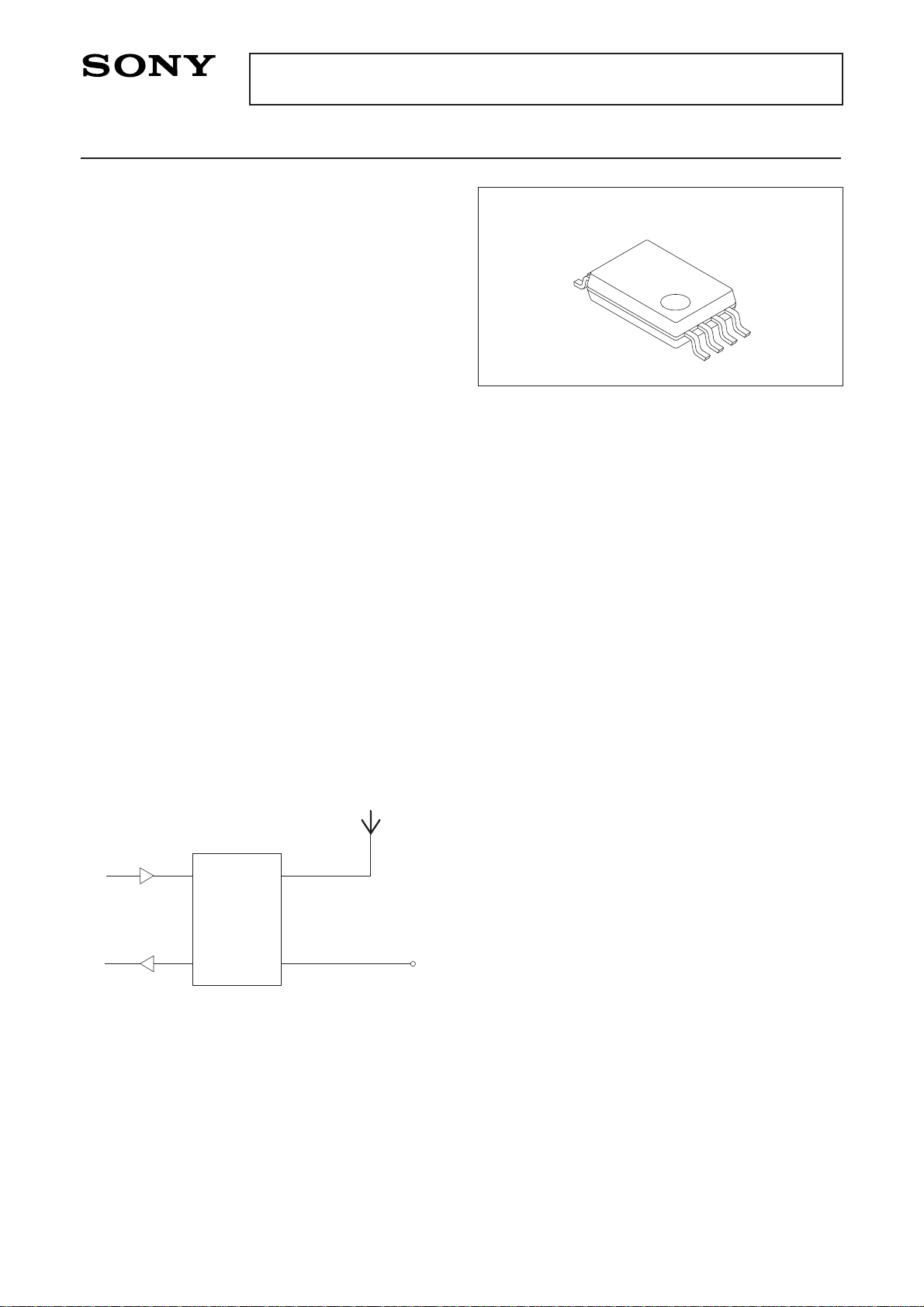
8 pin SSOP (Plastic)
E97756A79
GSM1800/1900 DPDT TX/RX Antenna Switch
Description
The CXG1017N is a high power DPDT switch
suitable for Digital Cellular applications. This device
is part of a growing family of MMIC Antenna switches
for digital cellular and cordless radios. It uses the
state-of-the-art Sony JFET process.
Features
• Positive voltage supply only
• Low insertion loss, typically 0.7dB at 33dBm input
level
• Stable Characteristics over wide temperature range
• Fast switching-100ns Typical
• Low current consumption, 400µA typical at 5.5V
• 8 pin SSOP package (3.0 × 6.4mm)
Applications
• GSM1800 handportable
• GSM1900 handportable
• DECT basestation/handportable diversity antenna
switching
• Other digital cellular and wireless local loop
applications
Typical Application
ESD
As with other GaAs semiconductors, ESD precautions
must be adhered to.
Sony reserves the right to change products and specifications without prior notice. This information does not convey any license by
any implication or otherwise under any patents or other right. Application circuits shown, if any, are typical examples illustrating the
operation of the devices. Sony cannot assume responsibility for any problems arising out of the use of these circuits.
TX IN
RX OUT
CXG1017N
PA
LNA
Internal
Antenna
External
Antenna
<For Europe and America>
For the availability of this product, please contact the sales office.
Page 2
– 2 –
CXG1017N
<For Europe and America>
Electrical Characteristics
Measurement Conditions, unless otherwise stated: Vctl (L) = 0V, Vctl (H) = 5.5V,
Pin = 33dBm GSM Burst (577µs pulse length with 8:1 Duty cycle), F = 1.75GHz. Temperature Range –25 to +75°C.
Parameter
Insertion loss
Isolation
VSWR
Switching time
Harmonic levels
Control currents
P0.1dB
P0.3dB
P0.1dB for Vctl (H) = 4.5V
P0.1dB for Vctl (H) = 3.0V
14
0.7
16
100
–56
400
34.5
35.5
34
29
0.95
1.5
–50
800
dB
dB
ns
dBc
µA
dBm
dBm
dBm
dBm
Min. Typ. Max. Unit
Control Voltage Selection, Vctl (H)
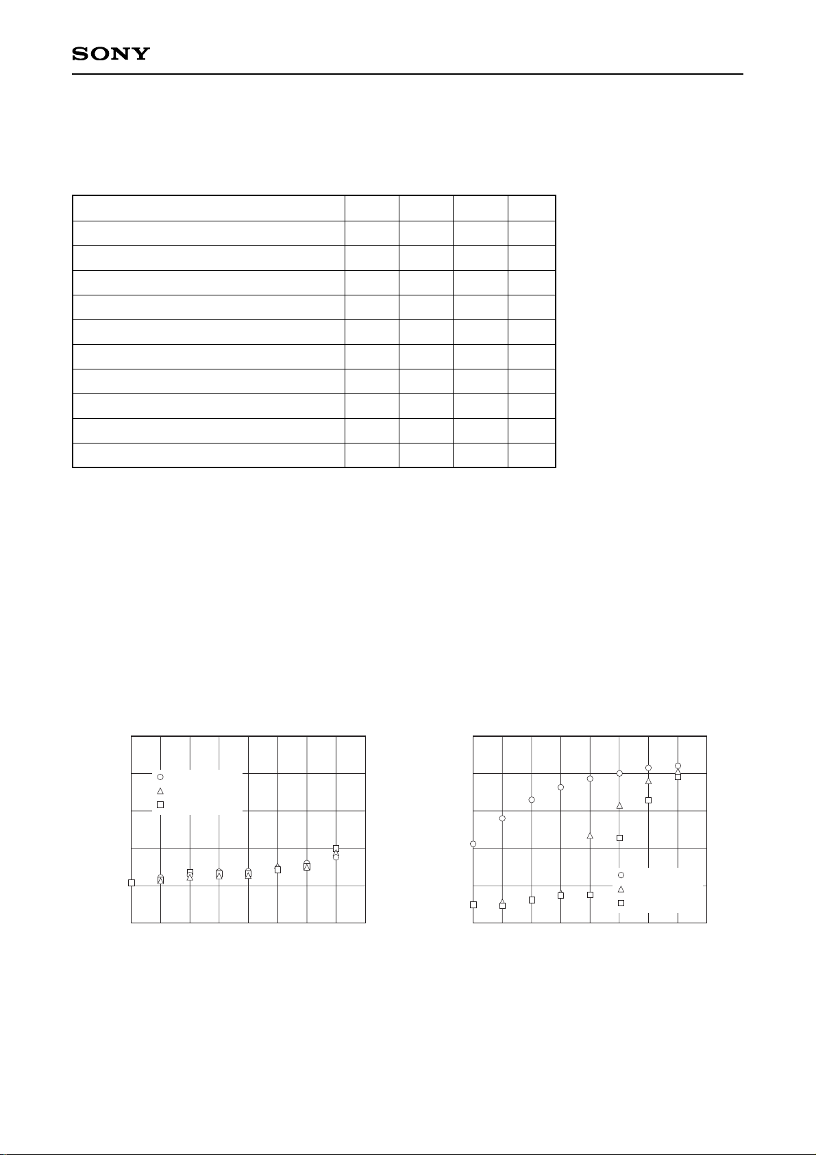
The choice of control voltage will determine the compression characteristic of the switch and the generation of
harmonics. The table above indicates the sensitivity of P0.1dB to control voltage, whilst the graphs below
indicate the sensitivity of harmonic levels:
Vctl = 0/3V
Vctl = 0/4.5V
Vctl = 0/5.5V
–20
–30
–40
–50
–60
–70
30 31 32 33 34 35 36 37 38
Input power [dBm]
2nd Harmonic with Power/Control Volts
Harmonic level [dBc]
Vctl = 0/3V
Vctl = 0/4.5V
Vctl = 0/5.5V
–20
–30
–40
–50
–60
–70
30 31 32 33 34 35 36 37 38
Input power [dBm]
3nd Harmonic with Power/Control Volts
Harmonic level [dBc]
Page 3
– 3 –
CXG1017N
<For Europe and America>
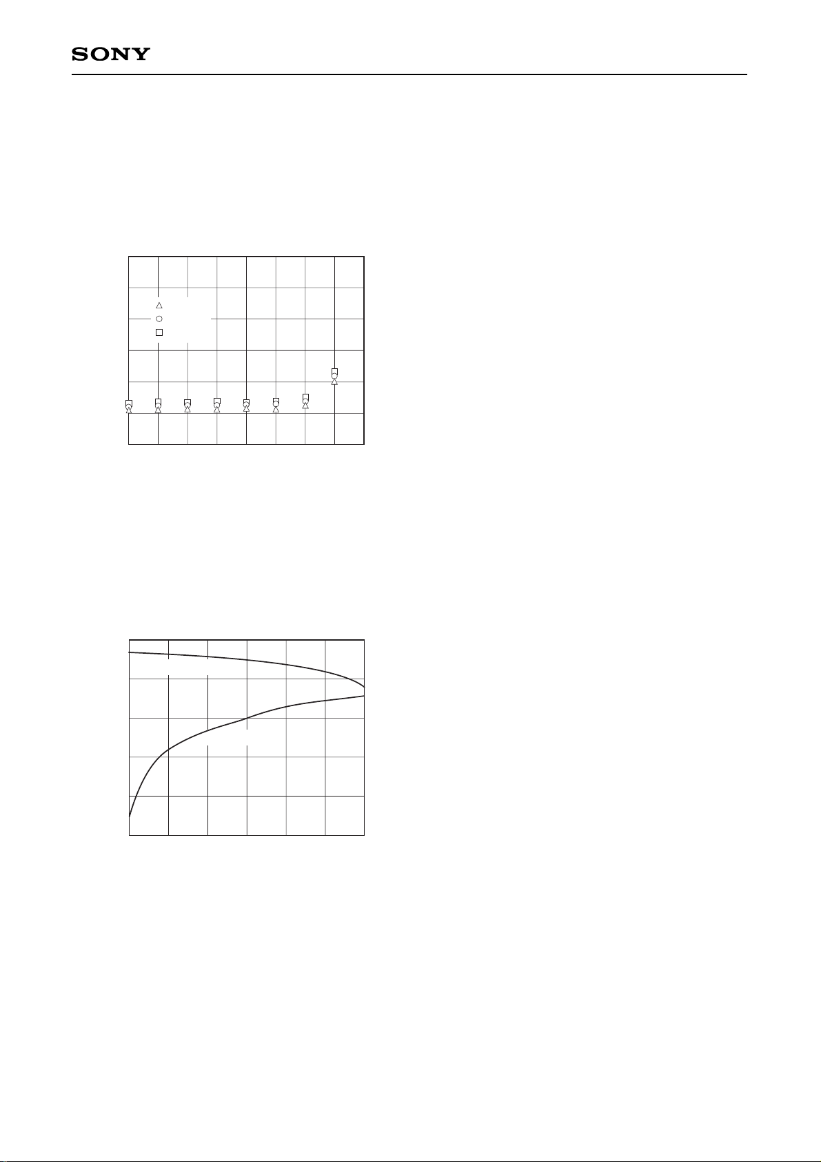
Compression Characteristics
Measurement Conditions: Vctl (L) = 0V, Vctl (H) = 5.5V, GSM Burst, F = 1.75GHz
Temperature range –25 to +75°C.
Typical Characteristics over Temperature:
–25°C
25°C
75°C
1.0
0.5
0
30 31 32 33 34 35 36 37 38
Input power [dBm]
Insertion loss [dB]
1.5
2.0
2.5
3.0
Frequency Characteristics
Measurement Conditions: Vctl (L) = 0V, Vctl (H) = 5.5V, Pin = 0dBm CW, T = 25°C
0
–1
–2
–3
–4
–5
0 1 2 3
Frequency [GHz]
Insertion Loss and Isolation vs. Frequency
Insertion loss [dB]
0
–10
–20
–30
–40
–50
Isolation [dB]
Insertion loss
Isolation
Page 4
– 4 –
CXG1017N
<For Europe and America>
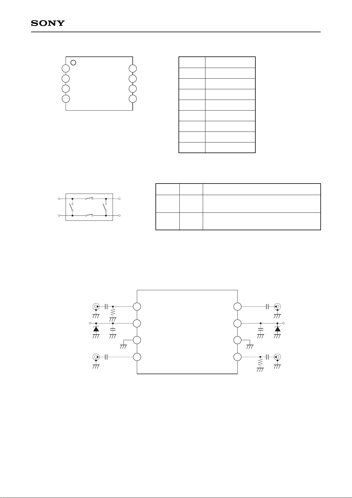
Schematic/Pinout
2
3
4
5
6
7
8
1
Port4
CTLB
GND
Port3
Port1
CTLA
GND
Port2
8pin SSOP (PLASTIC)
Pin No.
1
2
3
4
5
6
7
8
RF PORT1
Ctl (A)
GROUND
RF PORT2
RF PORT3
GROUND
Ctl (B)
RF PORT4
FUNCTION
Block Diagram/Truth Table
Port4
Port3
Port1
Port2
VCTLA
High
Low
Low
High
Port1-Port2, Port3-Port4 ON
Port2-Port3, Port4-Port1 OFF
Port2-Port3, Port4-Port1 ON
Port1-Port2, Port3-Port4 OFF
VCTLB
External Circuitry
Port4
Port3
Port1
Port2
RRF
75kΩ
C2
100pF
D1
C1
100pF
C2
100pF
C2
100pF
D1
C1
100pF
C2
100pF
RRF
75kΩ
2
4
1
3
5
6
7
8
optional
→
→
optional
When using the CXG1017N, the following external components should be used:
C1: This is used for signal line filtering 100pF is recommended.
C2: This is used for RF De-coupling and must be used in all applications. 100pF is recommended.
Rrf: This resistor is used to stabilize the dc operating point at high power levels. A value of 75kΩ is
recommended.
D1: 6.2V Zenor diodes may be incorporated at the Control lines, as indicated, in order to give improved
ESD performance if necessary.
Note) Internal and External Antenna Connections should be
diagonally opposite (1-3, 2-4).
Page 5
– 5 –
CXG1017N
<For Europe and America>
ESD Precautions
As this is a GaAs MMIC, ESD precautions must be adhered to, as outlined in at standard Data Book.
Please contact Sony if detailed ESD performance data is required.
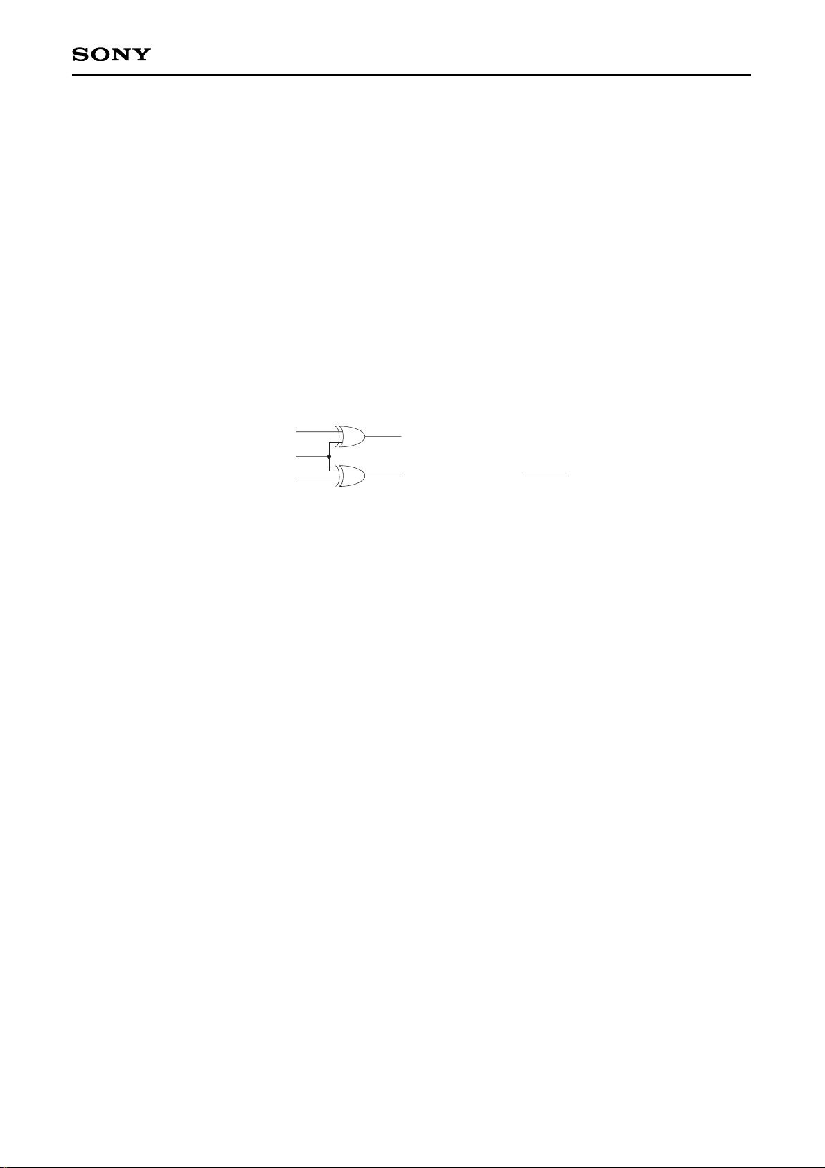
Configuration of External Logic Circuitry
For most portable appplicaitons, the following logic states are normally available.:
1. TX ON/OFF
2. RX ON/OFF
3. INT/EXT ANT.
A simple Logic circuit, using EXOR gates may be used to drive the CXG1017N. The following is a suggested
schematic:
CTLA
CTLB
TX ON/OFF
RX ON/OFF
INT/EXT ANT
A = TX ON/OFF
B = INT/EXT ANT
Port1 : INT ANT
Port2 : RX LNA
Port3 : EXT ANT
Port4 : TX PA
Assumed
Tape and Reel Information
This device is available in Tape and Reel. Order CXG1017N-T4
Reel Quantity: 1000 pieces/reel
Reel Dimensions: 245mm. There are detailed on Page 1-112 of the package manual 93.
Absolute Maximum Ratings (Ta = 25°C)
• Control voltage Vctl 7 V
• Operating temperature Topr –30 to +85 °C
• Storage temperature Tstg –65 to +150 °C
• Input Power Pin 37 dBm
Page 6
SAW
MCU
90MHz
I
Q
I
Q
AD
DA
Flash
Speech
Codec
LNA
SRAM
64K × 16
RX
PLL2PLL1
SGM2016AM-21-T7
IT362/IT402
IT363/IT403
IT413
CXG1037FN DCS1800
SPDT Antenna Switches
CXG1028TM GSM 900/1800/1900
CXG1006N GSM1800/1900
CXK5T8257BTM
CXK5T8512TM
CXK5T81000ATM
CXK5T16100TM
Sony IC
RX
TX
CAR ANTHP ANT
DSP
CXG1017N GSM1800/1900
CXA3021R
TX
32K × 8
64K × 8
128K × 8
64K × 16
– 6 –
CXG1017N
<For Europe and America>
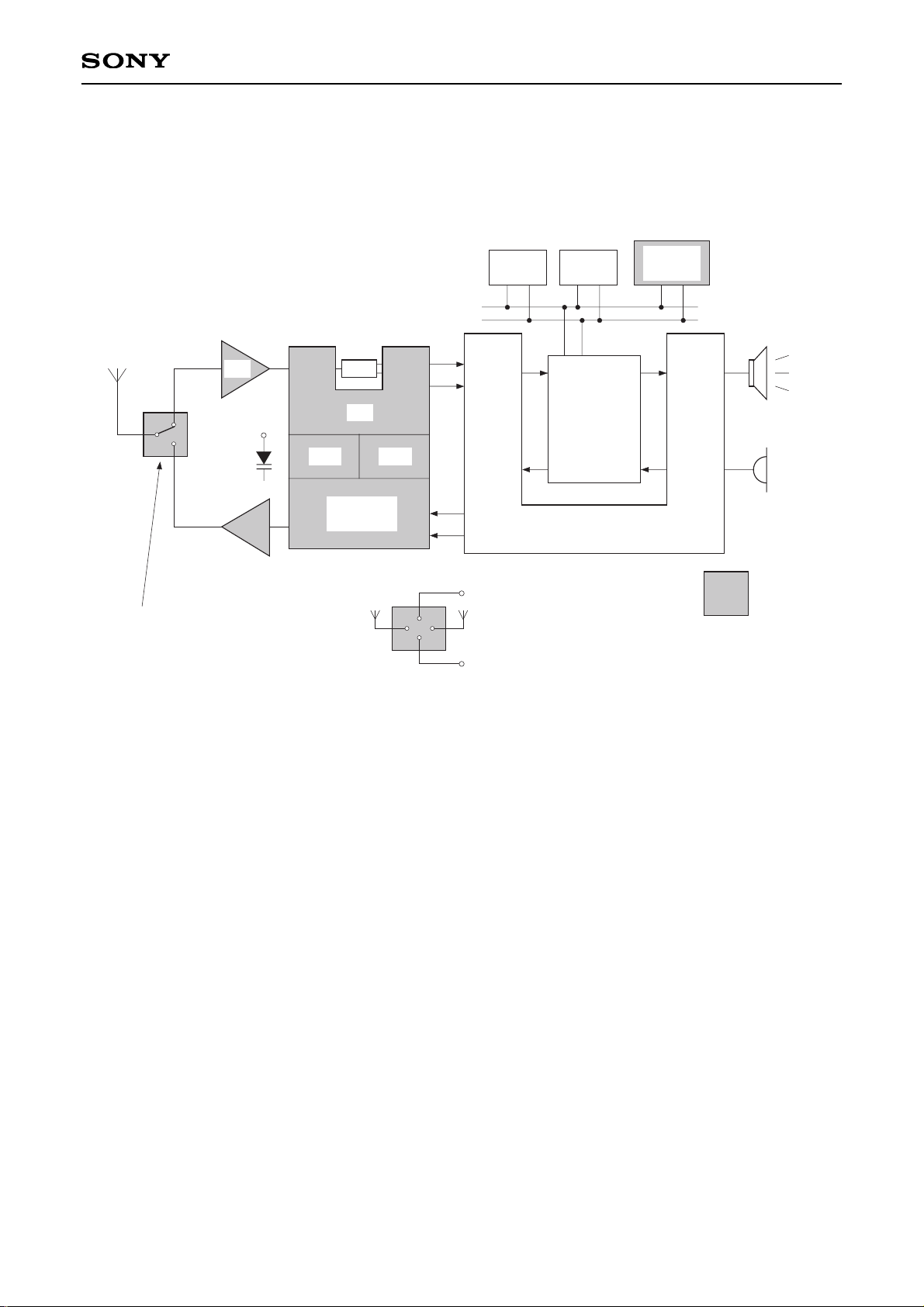
Sony GSM Lineup
Page 7

Package Outline Unit: mm
SONY CODE
EIAJ CODE
JEDEC CODE
PACKAGE MATERIAL
LEAD TREATMENT
LEAD MATERIAL
PACKAGE MASS
EPOXY RESIN
SOLDER / PALLADIUM
COPPER ALLOY
PACKAGE STRUCTURE
SSOP-8P-L01
PLATING
SSOP008-P-0044
0.04g
8PIN SSOP (PLASTIC)
0.24 – 0.07
+ 0.08
0.65
∗3.0 ± 0.1
∗4.4 ± 0.1
1.25 – 0.1
+ 0.2
0.1
A
6.4 ± 0.2
B
0.24 – 0.07
+ 0.08
(0.22)
0.17 – 0.015
+ 0.025
(0.15)
0.1 ± 0.05
0.25
0° to 10°
0.6 ± 0.15
(0.5)
1
4
58
0.13
M
DETAIL B
A
DETAIL
NOTE: Dimension “∗” does not include mold protrusion.
– 7 –
CXG1017N
<For Europe and America>
 Loading...