


SERVICE MANUAL
(without price)
ELECTRONIC CASH REGISTER
CE-3700 CE-3750
DEC, 1994
(EX-278)
(EX-279)
INDEX
|
CONTENTS |
|
|
|
Page |
1. |
SPECIFICATION .......................................................................................... |
1 |
2. |
OPTION SPECIFICATIONS ......................................................................... |
3 |
3. |
INSTALLATION ........................................................................................... |
3 |
4. |
INITIALIZE.................................................................................................... |
4 |
5. |
MAJOR COMPONENT ................................................................................ |
6 |
6. |
BLOCK DIAGRAM ....................................................................................... |
7 |
7. |
CIRCUIT EXPLANATIONS .......................................................................... |
8 |
8. |
DISASSEMBLY / ASSEMBLY METHOD .................................................. |
12 |
9. |
DIAGNOSTIC OPERATION ....................................................................... |
13 |
10. |
PROGRAMMING THE CE-3700 SERIES CASH REGISTERS ................. |
17 |
11. |
OPERATION .............................................................................................. |
19 |
12. |
ERROR CODES ......................................................................................... |
20 |
13. |
IC DATA ..................................................................................................... |
21 |
14. |
PCB LAYOUT ............................................................................................ |
22 |
15. |
CIRCUIT DIAGRAM ................................................................................... |
23 |
16. |
PARTS LIST ............................................................................................... |
33 |
Product introduction
This machine CE-3700(EX-278) is a succession machine for CE-3400(EX-253). The simultaneous boot model is EX-279.
EX-278: The drawer not separation type. EX-279: The drawer separation type.
The Rom/Ram is the internal organs.
1. SPECIFICATION
1-1. |
Product |
|
|
|
|
Operating temperature: |
0 °C |
~ |
40 °C |
|
Operation air moisture: |
10 % |
~ |
90 % |
|
Storage temperature: |
-25 °C |
~ |
65 °C |
|
Storage air moisture: |
10 % |
~ |
95 % |
|
Bombardment strength: |
To add bombardment from 10 high cm by single support, and there |
||
|
|
isn’t the problem. |
||
1-2. |
Package status |
|
|
|
|
Storage temperature: |
-25 °C |
~ |
65 °C |
|
Storage air moisture: |
10 % |
~ |
95 % |
|
Vibration strength: |
1.5 G |
|
|
|
Bombardment strength: |
To add bombardment from 60 high cm by single support, and there |
||
|
|
isn’t the problem. |
||
1-3. |
Accessory specifications |
|
|
|
|
Roll paper: |
P-4575 (EX-P-4574), 45 X 12 X 30 D |
||
|
Stamp logotype: |
CSP-2030ASA-2 |
||
|
Ink for supplement: |
Super Ink KC |
|
|
|
Ink roll: |
IR-92 (EX-INK-IR-92-OP) |
||
|
Dust cover: |
Only 1 part neighborhood |
||
1-4. |
Printer |
|
|
|
|
CR-812A-009-14-001A: |
Europe |
|
|
|
CR-812A-009-15-001A: |
USA, Canada, UK, Europe |
||
|
Printing type: |
ring select mode |
||
|
Output sheet number: |
2 |
|
|
|
Chart specifications |
|
|
|
|
Paper width: |
|
|
44.5 ± 0.5 mm |
|
Maximum paper diameter: |
|
Ø 83 mm |
|
|
Maximum paper thickness: |
|
0.06 ~ 0.085 mm |
|
|
Materials: |
|
|
Regular paper |
|
Inking: |
Ink roll |
|
|
|
Validation |
|
|
|
|
Print specifications: |
|
|
Yes |
|
Sensor: |
|
|
No |
|
Paper cut: |
Manual |
|
|
|
Stamp |
|
|
|
|
Color: |
|
|
Purple |
|
Seal side dimension: |
|
|
30 mm (W) X 20 mm (H) |
— 1 —

1-5. The durability specifications |
|
|
|
|
|
|
|
|
|
|
|
|
||||
|
Switch |
|
|
|
|
|
|
|
|
|
|
|
|
|
|
|
|
Key board switch: |
|
|
5,000,000 times |
|
|
|
|
|
|||||||
|
Control lock: |
|
|
20,000 times |
|
|
|
|
|
|
|
|||||
|
Operation key |
|
|
100,000 times |
|
|
|
|
|
|||||||
|
Feed switch |
|
|
5,000,000 times |
|
|
|
|
|
|||||||
|
Receipt on/off switch |
|
|
10,000 times |
|
|
|
|
|
|
|
|||||
|
Reset switch |
|
|
100,000 times |
|
|
|
|
|
|||||||
|
Drawer: |
|
|
|
|
|
|
|
|
|
|
|
|
|
|
|
|
|
|
|
|
|
|
1,000,000 times |
|
|
|
|
|
||||
|
Printer |
|
|
|
|
|
|
|
|
|
|
|
|
|
|
|
|
MCBF: |
|
|
|
|
|
2,000,000 line |
|
|
|
|
|
||||
|
Ink roll |
|
|
|
|
|
400,000 line |
|
|
|
|
|
|
|
||
|
Stamp |
|
|
|
|
|
|
|
|
|
|
|
|
|
|
|
|
Ink: |
|
|
|
|
|
50,000 times |
|
|
|
|
|
|
|
||
|
mechanism: |
|
|
500,000 times |
|
|
|
|
|
|||||||
1-6. |
Electric specifications |
|
|
|
|
|
|
|
|
|
|
|
|
|||
|
Power consumption |
|
|
|
|
|
|
|
|
|
|
|
|
|||
|
|
|
|
|
|
|
|
|
|
|
|
|
||||
|
|
Area |
|
|
120 V |
|
220 V |
230V |
|
240V |
||||||
|
|
|
|
|
|
|
|
|
|
|
|
|
|
|||
|
In action |
|
|
Max. |
|
|
0.40 A |
|
|
0.20 A |
|
0.20 A |
|
|
0.20 A |
|
|
In holding |
|
|
Min. |
|
|
0.09 A |
|
0.05 A |
0.05 A |
|
0.05 A |
||||
|
Power off |
|
|
0.08 A |
|
0.04 A |
0.04 A |
|
0.04 A |
|||||||
1-7. |
Memory Protection |
|
|
|
|
|
|
|
|
|
|
|
|
|||
|
Protection battery: |
Vanadium Lithium secondary battery |
|
|
||||||||||||
|
|
|
|
|
Model: VL3032/IF2 |
|
|
|
|
|
|
|
||||
|
Guard period: |
|
|
|
90 days (25 °C) In perfection charge status |
|
|
|||||||||
|
Galvanic cell life expectancy: |
|
5 years |
|
|
|
|
|
|
|
||||||
|
Recharge time: |
48 hours in secondary battery |
|
|
|
|
|
|||||||||
CAUTION
Danger of explosion if battery is incorrectly replaced. Replace only with the same or equivalent type recommended by the manufacturer.
Dispose of used batteries according to the manufacture’s instructions.
1-8. Clock, date facility |
|
|
Clock precision: |
Less than ±30 seconds (25 °C) |
|
|
Automatic calendar: |
Until 2099 |
1-9. Electric power supply for an emergency (B-6) |
|
|
Operating hour: |
3 hours |
|
Driving condition |
|
|
Processing time per customer one person: |
60 sec./ person |
|
Purchase item number: |
10 item / person |
|
1 item registration amount of money number of digits: 4 digits / item |
||
The handling number of people for 1 hour: |
30 person /hour |
|
Recharge time: |
8 hours |
|
— 2 —
2. OPTION SPECIFICATIONS
2-1. |
Ink roll: |
|
IR-92 |
|
|
|
2-2. |
Waterproofing cover: |
WT-70 |
|
|
||
2-3. |
Roll paper: |
|
P-4575 (45×12×75D) |
|
|
|
2-4. Electric power supply for an emergency: B-6 |
|
|
||||
|
The parts for adding B-6 are not equipped. They should be ordered separately from service department. |
|||||
|
The following parts are necessary to add B-6. |
|
|
|||
|
|
|
|
|
|
|
|
|
No. |
Code No. |
Parts Name |
Specification |
Q'ty |
|
|
|
|
|
|
|
|
|
Q1 |
2200 3577 |
Transistor |
2SA1015(GR,O,Y) |
1 |
|
|
ZD1 |
2310 8879 |
Zener diode |
RD18EB1 |
1 |
|
|
D6,D7 |
2301 0011 |
Diode |
1S2471 |
2 |
|
|
C5 |
2804 5476 |
Electrolytic capacitor |
50RE47 |
1 |
|
|
R2,R3,R5 |
2600 7313 |
Carbon film resistor |
R-25-10K-J |
3 |
|
|
R1 |
2600 5612 |
Carbon film resistor |
R-25-2K-J |
1 |
|
|
|
6221 4218 |
Connector sub assembly |
E311294-1(#22) |
1 |
2-5. |
Keyboard Conversion Kit: |
CVK-S2/-L2/-LLL2/-FS2 |
|
|
||
2-6. |
Ink for supplement |
Super ink K |
|
|
||
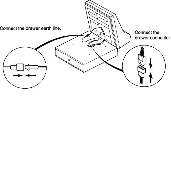
3. INSTALLATION
Connection is done of earth-line of drawer and main frame like lower chart.
— 3 —
4. INITIALIZE
By Initialize code
Init. A: The format is done of EEPROM, and, without it is read, and Init. Code is written in. Init. B: The data is read from EEPROM.
4-1. MAC
To hang initial start-up of CPU and peripheral device, and All Clear makes memory.
When there is Data backed up by EEPROM, by Initialize code, to develop it on Memory top.
Operation |
Display |
Printing |
Power off
To continued pushing J-feed button, and To set the MODE switch to Program.
To release from the
J-feed button.
D1 ~ D5
#-2
Header printing
0000000000
|
D1D2D3D4D5 |
XXXX: Rom Control No. |
|
|
|
|
|
-- XXXX -- |
|
|
D1D2D3D4D5 |
|
|
--------------- |
P1 |
0 |
|
Input value D1 ~ D5
D1 0: YYMMDD
1:MMDDYY
2:DDMMYY
D2 |
1: |
General |
(Add2, DDMMYY) |
|
|
|
|
2: |
US |
(Add2, MMDDYY) |
|
|
|
|
3: |
General |
(Add3, DDMMYY) |
|
|
|
|
5: |
Canada |
(Add2, MMDDYY) |
|
|
|
D3,D4 |
Department No. |
General |
15 |
|
|
|
|
|
|
|
US 30 |
|
|
D5 |
Clerk specification |
Switch: |
1,2,4 |
|
||
|
|
|
Password No.: |
0 |
(U.S.A. & Canada) |
|
Note: Operation code with Init.B is set up as with settlement in “00000”
— 4 —
4-2. Auto or Reset switch initialize |
|
||||
|
|
Operation |
Display |
||
|
|
|
0000000000 |
||
|
To push Reset SW. |
|
|||
|
|
or |
|
|
|
|
Power on In Low batt. |
|
|
||
|
|
|
|
|
D1D2D3D4D5 |
|
|
|
|
|
|
|
|
D1 ~ D5 |
|
|
|
|
|
|
|
|
|
#-2 |
P1 |
0 |
Input value D1 ~ D5
D1 0: YYMMDD
1:MMDDYY
2:DDMMYY
D2 |
1: |
General |
(Add2, DDMMYY) |
|
2: |
US |
(Add2, MMDDYY) |
|
3: |
General |
(Add3, DDMMYY) |
|
5: |
Canada |
(Add2, MMDDYY) |
D3,D4 |
Department No. |
General |
15 |
|
|
US |
30 |
D5 |
Clerk specification |
Switch: |
|
|
|
Password No.: |
|
Printing
XXXX:Rom Control No.
--XXXX --
D1D2D3D4D5
---------------
1,2,4
0 (U.S.A. & Canada)
Note: |
Operation code with Init.B is set up as with settlement in “00000”. |
4-3. Flag clear
To do Initialization of work memory, and make the operation sequence with the latest status.
Operation |
Display |
Printing |
Power off
To continued pushing R-feed button, and To set the MODE switch to Program.
To release from the
J-feed button.
#-2
Header printing
|
|
|
XXXX: Rom Control No. |
|
|
|
|
|
|
|
|
|
-- XXXX -- |
|
FFFFFFFFF |
|
D1D2D3D4D5 |
|
|
|
|
|
P1P2P3P4P5P6P7P8 |
|
|
|
|
X1X2X3X4 |
|
|
|
|
M1M2-D1D2-Y1Y2 |
|
|
|
|
--------------- |
|
|
|
|
Password for P1~P8 |
|
|
|
|
Password for X1~X4: |
|
|
|
|
X2/Z2 |
|
P1 |
0 |
|
M1M2D1D2Y1Y2 |
|
|
|
|
|
|
|
|
|
|
|
|
|
|
|
|
— 5 —

5. MAJOR COMPONENT
|
|
CPU |
|
|
UPD78044AGF080-3B9 |
|
|
|
|||
|
|
Ram |
|
|
LC36256PLL |
|
|
|
|
||
|
|
|
|
|
|
256K bit |
SRam |
|
|
|
|
|
|
Printer |
Model |
CR812A-009-15-001A |
|
|
|
||||
|
|
|
|
MCBF |
2,000,000 lines |
|
|
|
|
||
|
|
Drawer |
USA |
DL-2416 |
D-15TC-A55SP-1* |
|
|
||||
|
|
|
|
Canada |
DL-2351 |
D-15TC-A54SP-1* |
|
|
|||
|
|
|
|
UK |
|
DL-2751 |
D-15TC-A84SP-1* |
|
|
||
|
|
|
|
Other Countries |
DL-2350 |
D-15TC-A54P-1* |
|
|
|||
|
|
|
|
|
|
DL-2750 |
D-15TC-A84P-1* |
|
|
||
|
|
|
|
Germany |
DL-2752 |
D-15BC-A84S-1* |
|
|
|||
CPU Pin Description |
|
|
|
|
|
|
|
|
|||
Pin |
Port |
Name |
|
In/ |
Description |
Pin |
Port |
Name |
In/ |
Description |
|
No. |
No. |
|
|
Out |
|
|
No. |
No. |
|
Out |
|
|
|
|
|
|
|
|
|
|
|
|
|
1 |
94 |
FIP6 |
|
O |
Display Digit Signal (Dg7) |
41 |
32 |
TO2 |
O |
Receipt Common Signal |
|
2 |
93 |
FIP5 |
|
O |
Display Digit Signal (Dg6) |
42 |
31 |
TO1 |
O |
Auto cutter |
|
3 |
92 |
FIP4 |
|
O |
Display Digit Signal (Dg5) |
43 |
30 |
TO0 |
O |
Stamp |
|
4 |
91 |
FIP3 |
|
O |
Display Digit Signal (Dg4) |
44 |
3 |
INTP3 |
I |
Drawer sensor |
|
5 |
90 |
FIP2 |
|
O |
Display Digit Signal (Dg3) |
45 |
2 |
INTP2 |
I |
Key scan timing plus |
|
6 |
81 |
FIP1 |
|
O |
Display Digit Signal (Dg2) |
46 |
1 |
INTP1 |
I |
Power Down |
|
7 |
80 |
FIP0 |
|
O |
Display Digit Signal (Dg1) |
47 |
0 |
INTP0 |
I |
Printer |
|
8 |
|
|
|
|
Power (VDD) |
|
48 |
|
|
|
Gnd for Vpp (IC) |
9 |
27 |
SCK0 |
|
I/O |
Data 7 |
|
49 |
70 |
|
O |
Address decoder (A12/D0) |
10 |
26 |
SO1 |
|
I/O |
Data 6 |
|
50 |
71 |
|
O |
A13/Decod1 |
11 |
25 |
SI0 |
|
I/O |
Data 5 |
|
51 |
72 |
|
O |
A14/Decod1 |
12 |
24 |
BUSY |
|
I/O |
Data 4 |
|
52 |
|
|
|
Power (VDD) |
13 |
23 |
STB |
|
I/O |
Data 3 |
|
53 |
127 |
FIP33 |
O |
Printer Head (HD8) |
14 |
22 |
SCK1 |
|
I/O |
Data 2 |
|
54 |
126 |
FIP32 |
O |
Printer Head (HD7) |
15 |
21 |
SO1 |
|
I/O |
Data 1 |
|
55 |
125 |
FIP31 |
O |
Printer Head (HD6) |
16 |
20 |
SI1 |
|
I/O |
Data 0 |
|
56 |
124 |
FIP30 |
O |
Printer Head (HD5) |
17 |
|
|
|
|
Reset Signal |
|
57 |
123 |
FIP29 |
O |
Printer Head (HD4) |
18 |
74 |
|
|
O |
CE(Ram Chip Enable) |
58 |
122 |
FIP28 |
O |
Printer Head (HD3) |
|
19 |
73 |
|
|
O |
R/W(Ram Write Enable) |
59 |
121 |
FIP27 |
O |
Printer Head (HD2) |
|
|
|
|
|
|
Analog electric potential of AD |
|
|
|
|
|
|
20 |
|
|
|
|
converter (Gnd) |
|
60 |
120 |
FIP26 |
O |
Printer Head (HD1) |
21 |
17 |
ANI7 |
|
I |
Key Input Signal (KI7) |
61 |
117 |
FIP25 |
O |
Printer Head (HD10) |
|
22 |
16 |
ANI6 |
|
I |
Key Input Signal (KI6) |
62 |
116 |
FIP24 |
O |
Printer Head (HD9) |
|
23 |
15 |
ANI5 |
|
I |
Key Input Signal (KI5) |
63 |
115 |
FIP23 |
O |
Printer J-feed |
|
24 |
14 |
ANI4 |
|
I |
Key Input Signal (KI4) |
64 |
114 |
FIP22 |
O |
Printer R-feed |
|
25 |
13 |
ANI3 |
|
I |
Key Input Signal (KI3) |
65 |
113 |
FIP21 |
O |
Printer Motor |
|
26 |
12 |
ANI2 |
|
I |
Key Input Signal (KI2) |
66 |
112 |
FIP20 |
O |
Key Common Signal (KC9) |
|
|
|
|
|
|
|
|
|
|
|
|
Display Digit Signal / Key |
27 |
11 |
ANI1 |
|
I |
Key Input Signal (KI1) |
67 |
111 |
FIP19 |
O |
Common Signal (SGdb/KC8) |
|
|
|
|
|
|
|
|
|
|
|
|
Display Digit Signal / Key |
28 |
10 |
ANI0 |
|
I |
Key Input Signal (KI0) |
68 |
110 |
FIP18 |
O |
Common Signal (SGtr/KC7) |
|
|
|
|
|
|
Analog electric power supply of |
|
|
|
|
Display Digit Signal / Key |
|
29 |
|
|
|
|
AD converter (Vcc) |
|
69 |
107 |
FIP17 |
O |
Common Signal (SGg/KC6) |
|
|
|
|
|
Reference voltage input of AD |
|
|
|
|
Display Digit Signal / Key |
|
30 |
|
|
|
|
converter (Gnd) |
|
70 |
106 |
FIP16 |
O |
Common Signal (SGf/KC5) |
|
|
|
|
|
|
|
|
|
|
|
Pull Down electric potential for |
31 |
|
|
|
|
Clock Terminal |
|
71 |
|
|
|
Fip (VN) |
|
|
|
|
|
|
|
|
|
|
|
Display Digit Signal / Key |
32 |
|
|
|
|
Clock Terminal |
|
72 |
105 |
FIP15 |
O |
Common Signal (SGe/KC4) |
|
|
|
|
|
Analog electric potential of AD |
|
|
|
|
Display Digit Signal / Key |
|
33 |
|
|
|
|
converter(Gnd) |
|
73 |
104 |
FIP14 |
O |
Common Signal (SGd/KC3) |
|
|
|
|
|
|
|
|
|
|
|
Display Digit Signal / Key |
34 |
|
|
|
|
System Clock 4.19MHz |
74 |
103 |
FIP13 |
O |
Common Signal (SGc/KC2) |
|
|
|
|
|
|
|
|
|
|
|
|
Display Digit Signal / Key |
35 |
|
|
|
|
System Clock 4.19MHz |
75 |
102 |
FIP12 |
O |
Common Signal (SGb/KC1) |
|
|
|
|
|
|
|
|
|
|
|
|
Display Digit Signal / Key |
36 |
37 |
|
|
O |
EEPROM CE |
|
76 |
101 |
FIP11 |
O |
Common Signal (SGa/KC0) |
37 |
36 |
BUZ |
|
O |
Buzzer |
|
77 |
100 |
FIP10 |
O |
Key Scan Timing Plus |
38 |
35 |
PCL |
|
O |
Decoder CE |
|
78 |
97 |
FIP9 |
O |
Display Digit Signal (Dg10) |
39 |
34 |
TI2 |
|
O |
DW1&2 |
|
79 |
96 |
FIP8 |
O |
Display Digit Signal (Dg9) |
40 |
33 |
TI1 |
|
O |
Journal Common Signal |
80 |
95 |
FIP7 |
O |
Display Digit Signal (Dg8) |
|
— 6 —

6. BLOCK DIAGRAM
Standard |
CPU |
Option |
|
||
|
|
|
Printer (CR812A)
Main Display (10 columns)
Pop-uo Display
(10 columns)
RAM (32K byte)
EEPROM (512 byte)
Key board
Drawer |
|
Multi Drawer |
|
|
|
|
|
Compulsory Drawer
(USA, Canada,Germany, UK)
Buzzer
Power Supply
Back-up battery |
|
|
Battery operation |
(Vanadium Lithium) |
|
(B-6) |
|
|
|
|
|
— 7 —
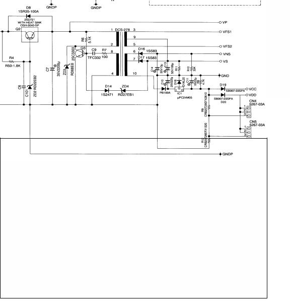
7. CIRCUIT EXPLANATIONS
7-1. Power supply circuit
1)Diodes rectification bridge
By diodes rectification bridge, alternating voltage is converted into DC voltage, and the electrical voltage is done filtering of by Capacitor C4.
2)Power supply circuit for B-6
The electrical voltage which puts in resistor 3 when line voltage includes anomaly changes, and transistor Q1 becomes on status, and CS signal is done outgoing of by this, and VP is supplied than Power supply B-6.
Note: The component for connection isn’t equipped with in plant shipping. (service arrangement)
7-2. DC/DC converter circuit
2SD721(Q2) is Power voltage control transistor, and electric power supply is supplied in DCDC converter with 2SC3303(Q3). 2SC3303(Q3) does a work as oscillator. The frequency of 2SC3303(Q3) is controlled by signal done feed back of through RD27EB1.
7-3. Electrical voltage value in check point
|
|
Vc |
Vp |
|
Vcc/Vdd |
|
Vns |
|
Vs |
|
Vf |
|
|
|
|
|
|
|
|
|
|
|
|
|
|
|
|
|
|
Rated output electrical voltage |
|
Min: 23 V |
20 V |
|
5 V |
|
32 V |
|
27 V |
|
4.75 |
V |
||
Output voltage drift range |
|
Max: 42 V |
|
2 V |
|
0.3 V |
|
10% |
|
10% |
|
7% |
|
|
Output voltage drift range |
|
AC |
DC |
|
DC |
|
DC |
|
DC |
|
AC |
|
|
|
— 8 —
7-4. Reset circuit
The voltage fluctuation of VDD is controlled of IC10 (S-80727AN).
CPU is done Reset by pushing Reset Switch or drifting VDD.
S-80727AN
Vdd
2 1
3
CPU
Reset SW
17
Reset
7-5. Data communication between CPU and EEPROM IC11(BR93LC46A).
EEPROM is Rom that write / erase is possible electrically.
BR93LC46A is a nonvolatile register, and serial data of 16 bit can be memorized with 64 register.
CPU |
|
|
EEPRom |
|
|
|
|
||
|
|
36 |
|
|
CS |
1 |
EEPCS |
||
2 |
14 |
|||
SK |
AD2 |
|||
3 |
15 |
|||
DI |
AD1 |
|||
4 |
16 |
|||
DO |
AD0 |
|||
|
|
|||
|
|
|
|
CS: |
Chip select |
SK: |
Serial data clock |
DI: |
Serial data input |
DO: |
Serial data output |
|
64 words X 16 bits 1,024 bits |
— 9 —
[ Data reading procedure ]
When the CPU read the data of EEPROM, CPU send the CS signal and SK signal to EEPROM. Then CPU send the address to EEPROM, and then EEPROM return the data to CPU.
CS |
|
SK |
|
DI |
Address |
DO |
Data |
|
|
|
Output data here |
[ Data writing procedure ]
When the CPU save the data to EEPROM, CPU sends the CS and SK signal to EEPROM. And CPU send the address and data to EEPROM from pin No. 15.
When the EEPROM writes the data, EEPROM outputs the busy signal form DO terminal to CPU. After finish writing, EEPROM outputs the ready signal from DO terminal to CPU.
Status
CS
SK
Address |
Data |
DI
READY(H)
DO
High Impedance
BUSY(L)
— 10 —

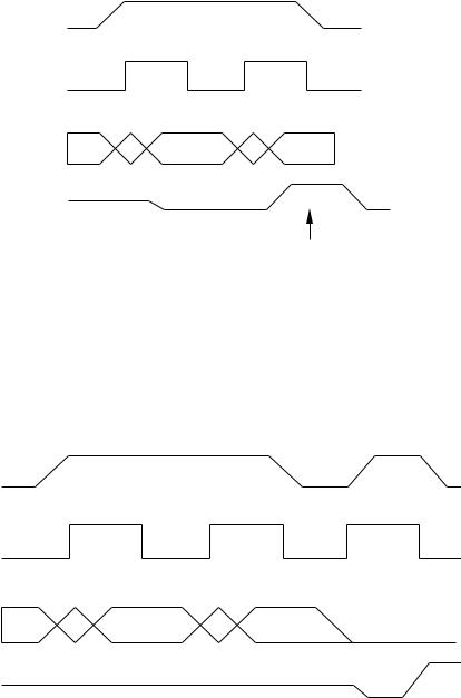
7-6. |
Time chart |
|
|
|
|
1) RAM writing timing |
|
|
|
|
|
|
16.4 us |
13.6us |
|
A0 |
WE |
|
3.95us |
|
A1 |
CE |
|
|
|
A2 |
D0 |
|
|
|
A3 |
D1 |
|
|
|
A4 |
D2 |
|
|
|
A5 |
D3 |
|
|
|
A6 |
D4 |
|
|
|
A7 |
D5 |
|
|
|
|
|
1.4us |
15.0us |
|
B2 |
A0 |
|
|
|
B3 |
|
|
|
|
B4 |
A1 |
|
|
|
B5 |
A2 |
|
|
|
B6 |
A3 |
|
|
|
B7 |
A4 |
|
|
|
B0 |
A6 |
|
|
|
B1 |
A7 |
|
|
|
2) RAM reading timing |
|
|
|
|
A0 |
WE |
|
|
|
A1 |
CE |
18.3us |
7.45us |
|
A2 |
D0 |
|
|
|
A3 |
D1 |
|
|
|
A4 |
D2 |
|
|
|
A5 |
D3 |
|
|
|
A6 |
D4 |
|
|
|
A7 |
D5 |
|
|
|
B2 |
A0 |
|
|
|
B3 |
|
|
|
|
B4 |
A1 |
|
|
|
B5 |
A2 |
|
|
|
B6 |
A3 |
|
|
|
B7 |
A4 |
|
|
|
B0 |
A6 |
|
|
|
B1 |
A7 |
|
|
3) EEP-ROM Writing and reading timing
29us
A0 CS
A1 SK
A2 DI
A3 DO
— 11 —
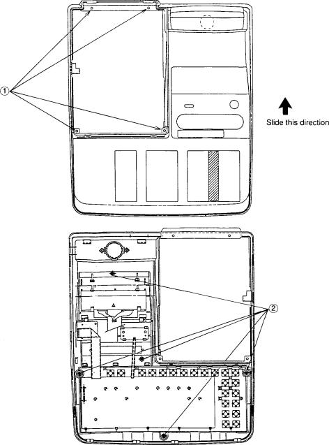
8.DISASSEMBLY / ASSEMBLY METHOD
1)Remove the Printer cover.
2)Upper case can remove it from by 4 places screws of printer four corners. (Lower chart 1 reference)
3)It comes off while sliding of Upper case backward by raising it.
4)Key board can remove it from by 4 places screws. (Lower chart 2 reference)
— 12 —

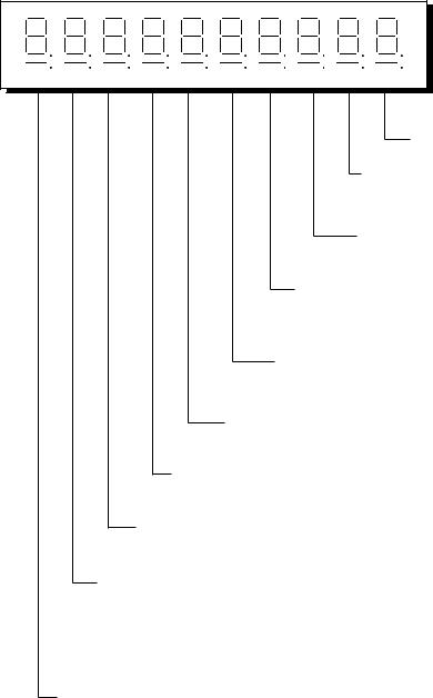
9. DIAGNOSTIC OPERATION
9-1. Start-up method
By the next operation, EX-278 enters Test mode.
1)Mode switch off.
2)To continued pushing J-feed button.
3)To set the Mode switch to Program.
4)To release from the J-feed button.
5)To input 9 9 9 9 9 0 0 0 0 0 #2
Printing out
00-00-00
00:00
0000
<Feed>
X: “Version No.” or “- - • • • • - -”
-- xxxx --
----------------
The cancellation of test mode do INIT.
9-2. Description
1)Key code representation: expect Value number, Clear and Feed button.
2)Various switches status display
|
|
3) Testing for Display, Print, DRW, RAM: |
|
Value number 1 column + #2 |
|
|
|
|||||||||||||||||||||
|
|
4) Testing for E2PROM: |
|
|
|
|
|
|
Value number 1 column + #2 |
|
|
|
||||||||||||||||
9-3. Key code representation |
|
|
|
|
|
|
|
|
|
|
|
|
|
|
|
|
|
|
||||||||||
|
|
RF |
|
JF |
|
062 |
|
C |
|
|
055 |
|
053 |
|
051 |
|
045 |
|
039 |
|
033 |
|
027 |
|
021 |
|
018 |
|
|
|
|
|
|
|
|
|
|
|
|
|
|
|
|
||||||||||||||
|
072 |
|
067 |
|
061 |
|
056 |
|
|
054 |
|
052 |
|
050 |
|
044 |
|
038 |
|
032 |
|
026 |
|
020 |
|
017 |
|
|
|
071 |
|
066 |
|
060 |
|
7 |
|
|
8 |
|
9 |
|
049 |
|
043 |
|
037 |
|
031 |
|
025 |
|
019 |
|
016 |
|
|
|
070 |
|
065 |
|
059 |
|
4 |
|
|
5 |
|
6 |
|
048 |
|
042 |
|
036 |
|
030 |
|
024 |
|
014 |
|
015 |
|
|
|
069 |
|
064 |
|
058 |
|
1 |
|
|
2 |
|
3 |
|
047 |
|
041 |
|
035 |
|
029 |
|
023 |
|
075 |
|
073 |
|
|
|
068 |
|
063 |
|
057 |
|
0 |
|
|
011 |
|
012 |
|
046 |
|
040 |
|
034 |
|
028 |
|
022 |
|
074 |
|
013 |
|
|
013: #1 key 014: #2 key
— 13 —
9-4. Various switch status display
0: Fixed
For Taiwan
1: Journal mark sensor 0: Except it
For Taiwan
1: Receipt mark sensor 0: Except it
1: Fixed
Non taxable pad For Japan 0: Taxable (pat short) 1: Non-taxable (pat open)
Drawer sensor
0: Open
1: Close
Journal near end
1: Near end
0: Out of sense
Receipt off switch
0:Receipt on
1:Receipt off
Key clerk
0:Non
1~9, A~F:Clerk code (Hexadecimal representation)
Push clerk
0:Non
1:Clerk 1
2:Clerk 2
3:Clerk 3
4:Clerk 4
Mode representation
1:PGM
2:RF
3:REG1
4:REG2
5:X
6:Z
7:X2Z2
8:Off
0: Disconnected
— 14 —
9-5. Print, Display, Drawer and Ram testing to do a various test by value number key. The following code print by all means then.
|
|
|
1 |
# |
|
1 #2: All testing |
|||||||||||||||||||||||||
|
|
|
|
||||||||||||||||||||||||||||
|
|
|
3 |
# |
|
3 #2: E2PRom r/w testing |
|||||||||||||||||||||||||
|
|
|
4 |
# |
|
4 #2: E2PRom reading testing |
|||||||||||||||||||||||||
|
|
|
5 |
# |
|
5 #2: Ram reading testing |
|||||||||||||||||||||||||
|
|
|
96 |
# |
|
96 #2:E2PRom Initialization |
|||||||||||||||||||||||||
|
|
|
8 |
# |
|
8 #2: Printing testing |
|||||||||||||||||||||||||
|
|
|
9 |
# |
|
9 #2: Clock testing |
|||||||||||||||||||||||||
|
|
|
|
|
|
|
|
|
|
|
|
|
|
|
|
|
|
|
|
|
|
|
|
|
|
|
|
|
|
|
|
|
|
|
|
|
|
|
|
|
|
|
|
|
|
|
|
|
|
|
|
|
|
|
|
|
|
|
|
|
|
|
|
1) |
|
|
|
|
|
|
All lighting, Ram, R/W, setting the time and date, drawer |
||||||||||||||||||||||||
1 |
|
|
#2 |
|
|||||||||||||||||||||||||||
|
|
|
|
opening, printing, receipt(Japan) stamp and receipt issue. |
|||||||||||||||||||||||||||
|
|
|
|
|
|
|
|||||||||||||||||||||||||
|
|
|
|
|
|
|
|
|
|
|
|
|
|
|
|
|
|
|
|
|
|
|
|
|
|
|
|
|
|
|
|
|
|
|
|
|
|
|
|
|
|
|
|
|
|
|
|
|
|
|
|
|
|
|
|
|
|
|
|
|
|
|
|
|
|
|
|
|
|
|
|
|
|
|
|
|
|
|
|
|
|
|
|
|
|
|
|
|
|
|
|
|
|
|
|
|
|
|
|
|
|
|
|
|
|
|
|
|
|
|
|
|
|
|
|
|
|
|
|
|
|
|
|
|
|
|
|
|
|
|
|
|
|
|
|
|
|
|
|
|
|
|
|
|
|
|
|
|
|
|
|
|
|
|
|
|
|
|
|
|
|
|
|
|
|
|
|
|
|
|
|
|
|
|
|
|
|
|
|
|
|
|
|
|
|
|
|
|
|
|
|
|
|
|
|
|
|
|
|
|
|
|
|
|
|
|
|
|
|
|
|
|
|
|
|
|
|
|
|
|
|
|
|
Display: |
All lighting |
|
|
|
|
|
Ram: R/W |
|
|
|
|
|
|
|
normal end: |
To be continued |
||||
|
Abnormal end: |
To do the following printing then breaking |
||||
|
|
|
|
|
|
|
|
|
|
|
- - - - - - - 2 |
|
|
|
|
|
|
|
|
|
|
|
|
|
|
|
|
|
|
|
|
|
|
|
Receipt printing
Beeping one shot buzzer on
Setting date and time:
Date: Dec. 31st 1994
Time: 23:59
Drawer open:
Drawer No.1 and No.2 are opened.
Test printing:
To do the following print
The first line does print in receipt, journal independence.
The second line does print at receipt, journal same time.
01234567FS@
01234567FS@
Receipt stamp: (only japan)
Receipt issue:
Testing display: To do indication as follows till key or a state changes
1234567890
— 15 —
2)
3 #2
Abnormal end:
3)
4 #2
This does R/W test of testing area of E2PRom during single word, and, at the time of normal, does normal termination print.
To do the following printing then breaking
- - - - - - - 8
Receipt printing
Beeping one shot buzzer on
This does read only test of testing area of EEPRom during single word. This test is continued till off mode or electric power supply enters it.
|
|
|
Abnormal end: |
To do the following printing then breaking |
||||||||
|
|
|
|
|
|
|
|
|
|
|
|
|
|
|
|
|
|
|
|
|
|
|
- - - - - - - 8 |
|
|
|
|
|
|
|
|
|
|
|
|
|
|
|
|
|
|
|
|
|
|
|
|
|
|
|
|
|
|
|
|
|
|
|
|
|
|
|
|
|
|
|
|
|
|
|
|
|
|
Receipt printing |
|||
|
|
|
|
|
|
|
|
|
Beeping one shot buzzer on |
|||
4) |
|
|
|
|
|
|
Read only test . |
|||||
|
5 |
|
#2 |
|||||||||
|
|
|
|
|
Outside Ram(0000H~7FFFH) read in testing |
|||||||
|
|
|
|
|
|
|
||||||
|
|
|
|
|
|
|
The address comparing data which comes under it |
|||||
|
|
|
|
|
|
|||||||
|
|
|
|
|
|
|
= (A0-A7) + (A8-A14) |
|||||
|
|
|
|
|
|
|
This test is continued till off mode or electric power supply enters it. |
|||||
|
|
|
Abnormal end: |
To do the following printing then breaking |
||||||||
|
|
|
|
|
|
|
|
|
|
|
|
|
|
|
|
|
|
|
|
|
|
|
- - - - - - - 2 |
|
|
|
|
|
|
|
|
|
|
|
|
|
|
|
|
|
|
|
|
|
|
|
|
|
|
|
|
|
|
|
|
|
|
|
|
|
|
|
|
|
|
|
|
|
|
|
|
|
|
Receipt printing |
|||
|
|
|
|
|
|
|
|
|
Beeping one shot buzzer on |
|||
5) |
|
|
|
|
|
|
|
Blanking (OFFH writing) of data in EEPRom entirely. |
||||
|
9 |
|
6 |
|
#2 |
|||||||
|
|
|
|
Time of day, a date are turned into zero entirely. |
||||||||
|
|
|
|
|
|
|
|
|||||
|
|
|
|
|
|
|
|
|
|
|
|
|
6) |
|
|
|
|
|
|
All time ring print testing |
|||||
8 |
|
#2 |
|
|||||||||
|
|
|
|
|
|
|
|
|
||||
|
|
|
|
|
|
|
|
|
|
|
|
|
|
|
|
|
|
|
|
|
|
|
- - - - - - - 2 |
|
|
|
|
|
|
|
|
|
|
|
|
|
|
|
|
|
|
|
|
|
|
|
|
|
|
|
|
|
|
|
|
|
|
|
|
|
|
Receipt printing |
||
7) |
|
|
|
|
|
|
Time of day representation testing |
|||||
9 |
|
#2 |
|
|||||||||
|
|
|
|
|
|
|
|
|
||||
|
|
|
|
|
|
|
|
|
|
|
|
|
Time of day indication is done till clear Key
23 -59 12
— 16 —
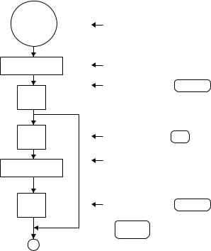
10. PROGRAMMING THE CE-3700 SERIES CASH REGISTERS
The Casio CE-3700 series is capable of a versatile range of features and function that give it the capability to readily adapt to almost any retail environment. The cash register is programmed at the factory with the most standard operating features and functions. Your local business requirements, however, may call for other functions of a totally different keyboard layout.
This section explains the different functions available, as well as the procedures that you can use to tailor the cash register to specific needs. Programming is simplified through the use of worksheets for each function, and step-by-step flow charts that walk you through each procedure.
10-1. Setting the proper MODE for programming
• Program Modes and feature
Mode |
Purpose |
Mode indicator |
|
Program 4 |
Assignment of 89 functions to programmable keys to create the |
P4 |
|
desired keyboard layout |
|||
|
|
||
Program 3 |
Definition of machine features and key functions that enhance |
P3 |
|
printing, totalizing, reporting and overall operation |
|||
|
|
||
Program 1 |
Programming of time, date and unit prices, amounts, rates, etc. |
P1 |
|
for enhanced security and automatic registration |
|||
|
|
You should perform the procedure shown blow as the first step of programming. Notice that the flowchart ends with an arrow on the bottom. This indicates that you should continue to the next programming procedure for the mode you specify.
• Procedure
Program
Program mode
Sub
Total
#1* Key
Program mode
Sub
Total
Set the Mode switch to Program
Enter a number to specify the program mode (1 ~ 4)
Press the Sub total key.
The display should show the letter “P” followed by the program number you specified (i.e. P3 = Program mode 3).
Press the # 1 key.
Enter 4-digit password.
Skip this step when the password is not programmed.
Press the Sub total key.
CA/Amt
Tend
key on standard keyboard.
Note: Program mode 1 is automatically set when the Mode switch is set to Program from another setting.
•Recommended programming sequence
Generally, you should perform programming in the following sequence. Note that we recommend you check what is programmed for each mode before proceeding to the programming operation.
—17 —
 Loading...