


ATMEL AT90LS2343-4SI, AT90LS2343-4SC, AT90LS2343-4PI, AT90LS2343-4PC, AT90S2343-10SI Datasheet
...Features
•Utilizes the AVR ® Enhanced RISC Architecture
•AVR - High Performance and Low Power RISC Architecture
•118 Powerful Instructions - Most Single Clock Cycle Execution
•2K bytes of In-System Programmable ISP Flash
–SPI Serial Interface for In-System Programming
–Endurance: 1,000 Write/Erase Cycles
•128 bytes EEPROM
–Endurance: 100,000 Write/Erase Cycles
•128 bytes Internal RAM
•32 x 8 General Purpose Working Registers
–3 AT90S/LS2323 Programmable I/O Lines
–5 AT90S/LS2343 Programmable I/O Lines
•VCC: 4.0 - 6.0V AT90S2323/AT90S2343
•VCC: 2.7 - 6.0V AT90LS2323/AT90LS2343
•Power-On Reset Circuit
•Speed Grades: 0 - 10 MHz AT90S2323/AT90S2343
•Speed Grades: 0 - 4 MHz AT90LS2323/AT90LS2343
•Up to 10 MIPS Throughput at 10 MHz
•One 8-Bit Timer/Counter with Separate Prescaler
•External and Internal Interrupt Sources
•Programmable Watchdog Timer with On-Chip Oscillator
•Low Power Idle and Power Down Modes
•Programming Lock for Flash Program and EEPROM Data Security
•Selectable On-Chip RC Oscillator
•8-Pin Device
Description
The AT90S/LS2323 and AT90S/LS2343 is a low-power CMOS 8-bit microcontrollers based on the AVR ® enhanced RISC architecture. By executing powerful instructions in a single clock cycle, the AT90S/LS2323 and AT90S/LS2343 achieves throughputs approaching 1 MIPS per MHz allowing the system designer to optimize power consumption versus processing speed.
The AVR core combines a rich instruction set with 32 general purpose working registers. All the 32 registers are directly connected to the Arithmetic Logic Unit (ALU), allowing two independent registers to be accessed in one single instruction executed in one clock cycle. The resulting architecture is more code efficient while achieving throughputs up to ten times faster than conventional CISC microcontrollers.
Pin Configuration
|
|
|
|
|
|
|
PDIP/SOIC |
|
|
|
|
|
||
|
|
|
|
|
|
|
|
|
|
|
|
|
|
|
|
|
|
|
|
|
|
|
|
|
|
|
|
|
|
RESET |
|
1 |
8 |
|
VCC |
RESET |
|
1 |
8 |
|
VCC |
|||
|
|
|
|
|||||||||||
(CLOCK) PB3 |
|
2 |
7 |
|
PB2 (SCK/T0) |
XTAL1 |
|
2 |
7 |
|
PB2 (SCK/T0) |
|||
|
|
|
||||||||||||
|
|
|
|
|||||||||||
|
PB4 |
|
3 |
6 |
|
PB1 (MISO/INT0) |
XTAL2 |
|
3 |
6 |
|
PB1 (MISO/INT0) |
||
|
|
|
|
|||||||||||
|
GND |
|
4 |
5 |
|
PB0 (MOSI) |
GND |
|
4 |
5 |
|
PB0 (MOSI) |
||
|
|
|
|
|||||||||||
|
|
|
|
|
|
|
|
|
|
|
|
|
||
|
|
|
AT90S/LS2343 |
|
|
|
AT90S/LS2323 |
|
||||||
8-Bit |
Microcontroller |
with 2K Bytes of |
In-System |
Programmable |
Flash |
AT90S2323 |
AT90LS2323 |
AT90S2343 |
AT90LS2343 |
Preliminary |
Rev. 1004AS–05/98 |
Note: This is a summary document. For the complete 34 page document, please visit our website at www.atmel.com or e-mail at 1 literature@atmel.com and request literature #1004A.
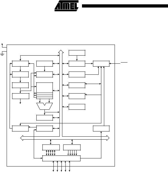
Block Diagram
Figure 1. The AT90S/LS2343 Block Diagram
VCC |
|
|
|
|
|
|
8-BIT DATA BUS |
|
|
||
|
|
INTERNAL |
|
|
|
|
|
OSCILLATOR |
|
|
|
GND |
|
|
|
|
|
PROGRAM |
STACK |
WATCHDOG |
TIMING AND |
RESET |
|
COUNTER |
POINTER |
TIMER |
CONTROL |
||
|
|||||
PROGRAM |
SRAM |
MCU CONTROL |
|
|
|
FLASH |
REGISTER |
|
|
||
|
|
|
|||
INSTRUCTION |
GENERAL |
TIMER/ |
|
|
|
REGISTER |
PURPOSE |
COUNTER |
|
|
|
|
REGISTERS |
|
|
|
|
INSTRUCTION |
X |
INTERRUPT |
|
|
|
Y |
|
|
|||
DECODER |
Z |
UNIT |
|
|
|
CONTROL |
ALU |
EEPROM |
|
|
|
LINES |
|
|
|||
|
|
|
|
||
|
STATUS |
|
|
|
|
|
REGISTER |
|
|
|
|
PROGRAMMING |
SPI |
|
OSCILLATOR |
|
|
LOGIC |
|
|
|||
|
|
|
|
||
|
DATA REGISTER |
DATA DIR. |
|
|
|
|
PORTB |
REG. PORTB |
|
|
|
|
PORTB DRIVERS |
|
|
||
|
PB0 - PB4 |
|
|
||
2 |
AT90S/LS2323 and AT90S/LS2343 |
|
|
||
|

AT90S/LS2323 and AT90S/LS2343
Figure 2. The AT90S/LS2323 Block Diagram
VCC |
|
|
|
|
|
|
8-BIT DATA BUS |
|
|
||
|
|
INTERNAL |
|
|
|
|
|
OSCILLATOR |
|
|
|
GND |
|
|
|
|
|
PROGRAM |
STACK |
WATCHDOG |
TIMING AND |
RESET |
|
COUNTER |
POINTER |
TIMER |
CONTROL |
||
|
|||||
PROGRAM |
SRAM |
MCU CONTROL |
|
|
|
FLASH |
REGISTER |
|
|
||
|
|
|
|||
INSTRUCTION |
GENERAL |
TIMER/ |
|
|
|
REGISTER |
PURPOSE |
COUNTER |
|
|
|
|
REGISTERS |
|
|
|
|
INSTRUCTION |
X |
INTERRUPT |
|
|
|
Y |
|
|
|||
DECODER |
Z |
UNIT |
|
|
|
CONTROL |
ALU |
EEPROM |
|
|
|
LINES |
|
|
|||
|
|
|
|
||
|
STATUS |
|
|
|
|
|
REGISTER |
|
|
|
|
PROGRAMMING |
SPI |
|
OSCILLATOR |
|
|
LOGIC |
|
|
|||
|
|
|
|
||
|
DATA REGISTER |
DATA DIR. |
|
|
|
|
PORTB |
REG. PORTB |
|
|
|
|
PORTB DRIVERS |
|
|
||
|
PB0 - PB2 |
|
|
||
Description
The AT90S/LS2323 and AT90S/LS2343 provides the following features: 2K bytes of In-System Programmable Fl ash, 1 28 bytes EE PRO M, 128 by tes S RAM, 3 (AT90S/LS2323) / 5 (AT90S/LS2343) general purpose I/O lines, 32 general purpose working registers, an 8-bit timer/counter, internal and external interrupts, programmable Watchdog Timer with internal oscillator, an SPI serial port for Flash Memory downloading and two software selectable power saving modes. The Idle Mode stops the CPU while allowing the SRAM, timer/counters, SPI port and interrupt system to continue functioning. The power down mode saves the register contents but freezes the oscillator, disabling all other chip functions until the next interrupt or hardware reset.
The device is manufactured using Atmel’s high density non-volatile memory technology. The on-chip Flash allows the program memory to be reprogrammed in-system through an SPI serial interface. By combining an 8-bit RISC CPU with ISP Flash on a monolithic chip, the Atmel AT90S/LS2323 and AT90S/LS2343 is a powerful micro-
controller that provides a highly flexible and cost effective solution to many embedded control applications.
The AT90S/LS2323 and AT90S/LS2343 AVR is supported with a full suite of program and system development tools including: C compilers, macro assemblers, program debugger/simulators, in-circuit emulators, and evaluation kits.
Comparison Between AT90S/LS2323
and AT90S/LS2343
The AT90S/LS2323 is intended for use with external quartz crystal or ceramic resonator as the clock source. The startup time is fuse selectable as either 1 ms (suitable for ceramic resonator) or 16 ms (suitable for crystal). The device has three I/0 pins.
The AT90S/LS2343 is intended for use with either an external clock source or the internal RC oscillator as clock source. The device has five I/0 pins.
3
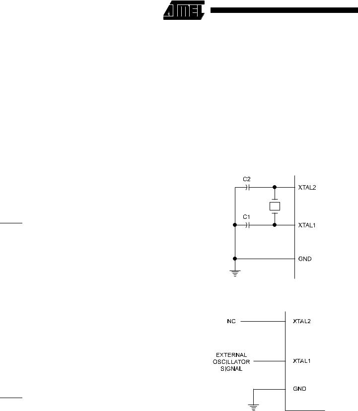
Table 1 summarizes the differences in features of the two devices.
Table 1. Feature Difference Summary
Part |
AT90S/LS2323 |
AT90S/LS2343 |
|
|
|
|
|
On-chip oscillator |
yes |
no |
|
amplifier |
|||
|
|
||
|
|
|
|
Internal RC Clock |
no |
yes |
|
|
|
|
|
PB3 usable |
never |
internal clock mode |
|
|
|
|
|
PB4 usable |
never |
always |
|
|
|
|
|
Startup time |
1 ms / 16 ms |
16 μs fixed |
|
|
|
|
Pin Descriptions AT90S/LS2323
VCC
Supply voltage pin.
GND
Ground pin.
Port B (PB2..PB0)
Port B is a 3-bit bi-directional I/O port. Port pins can provide internal pull-up resistors (selected for each bit).
RESET
Reset input. A low on this pin for two machine cycles while the oscillator is running resets the device.
XTAL1
Input to the inverting oscillator amplifier and input to the internal clock operating circuit.
XTAL2
Output from the inverting oscillator amplifier.
Pin Descriptions AT90S/LS2343
VCC
Supply voltage pin.
GND
Ground pin.
Port B (PB4..PB0)
Port B is a 5-bit bi-directional I/O port. Port pins can provide internal pull-up resistors (selected for each bit). When the device is clocked from an external clock source, PB3 is used as the clock input.
RESET
Reset input. A low on this pin for two machine cycles while the oscillator is running resets the device.
CLOCK
Clock signal input in external clock mode.
Clock Sources
The AT90S/LS2323 contains an inverting amplifier which can be configured for use as an on-chip oscillator, as shown in Figure 3. XTAL1 and XTAL2 are input and output respectively. Either a quartz crystal or a ceramic resonator may be used. It is recommended to use the AT90S/LS2343 if an external clock source is used, since this gives an extra I/O pin.
The AT90S/LS2343 can be clocked by an external clock signal, as shown in Figure 4, or by the on-chip RC oscillator. This RC oscillator runs at a nominal frequency of 1 MHz (VCC = 5V). A fuse bit - RCEN - in the Flash memory selects the on-chip RC oscillator as the clock source when programmed ('0'). The AT90S/LS2343 is shipped with this bit programmed.
Figure 3. Oscillator Connection
Figure 4. External Clock Drive Configuration
4 |
AT90S/LS2323 and AT90S/LS2343 |
|
|
||
|
 Loading...