


SDHC Card series
4~32GB High Capacity Secure Digital Card
Description |
|
Features |
|
Transcend High Capacity SD Card series are |
• |
RoHS compliant product. |
|
specifically designed to meet the High Capacity, High |
• |
Card Lid material: PC (comply with UL94,Flame |
|
Definition Audio and Video requirement for the latest |
Class:HB) |
||
Digital Cameras, DV Recorders, Mobile Phones, etc,. |
• |
Operating Voltage: 2.7 ~ 3.6V |
|
The new defined Speed Class enables the host to |
• |
Operating Temperature: -25 ~ 85°C |
|
support AV applications to perform real time |
• |
Durability: 10,000 insertion/removal cycles |
|
recording to the SD memory card. |
• |
Compatible with SD Specification Ver. 2.0 |
|
|
|
• |
Comply with SD File System Specification Ver. 2.0 |
Placement |
|
• |
Mechanical Write Protection Switch |
|
|
• |
Supports Speed Class Specification up to Class 2 |
|
|
• |
Supports Copy Protection for Recorded Media (CPRM) |
|
|
for SD-Audio |
|
|
|
• |
Seamless compatibility with SDMI-compliant digital audio |
|
|
devices |
|
|
|
• |
Form Factor: 24mm x 32mm x 2.1mm |
Front |
Back |
|
|
Pin Definition
Pin No. |
|
|
SD Mode |
|
|
SPI Mode |
|
|
|
|
|||
Name |
Type |
Description |
|
Type |
Description |
|
|
|
|||||
1 |
CD/DAT |
I/O/PP3 |
Card Detect/Data Line [Bit3] |
CS |
I |
Chip Select (neg true) |
2 |
CMD |
PP |
Command/Response |
DI |
I |
Data In |
3 |
VSS1 |
S |
Supply voltage ground |
VSS |
S |
Supply voltage ground |
4 |
VDD |
S |
Supply voltage |
VDD |
S |
Supply voltage |
5 |
CLK |
I |
Clock |
SCLK |
I |
Clock |
6 |
VSS2 |
S |
Supply voltage ground |
VSS2 |
S |
Supply voltage ground |
7 |
DAT0 |
I/O/PP |
Data Line [Bit0] |
DO |
O/PP |
Data Out |
8 |
DAT1 |
I/O/PP |
Data Line [Bit1] |
RSV |
|
|
9 |
DAT2 |
I/O/PP |
Data Line [Bit2] |
RSV |
|
|
Transcend Information Inc. |
1 |

SDHC Card series
4~32GB High Capacity Secure Digital Card
Architecture
Transcend Information Inc. |
2 |

SDHC Card series
4~32GB High Capacity Secure Digital Card
Bus Operating Conditions
• General
Parameter |
Symbol |
|
Min. |
Max. |
Unit |
Peak voltage on all lines |
|
-0.3 |
VDD+0.3 |
V |
|
All Inputs |
|
|
|
|
|
Input Leakage Current |
|
|
-10 |
10 |
µA |
All Outputs |
|
|
|
|
|
Output Leakage Current |
|
|
-10 |
10 |
µA |
• Power Supply Voltage
Parameter |
Symbol |
Min. |
Max. |
Unit |
|
Supply voltage |
VDD |
2.7 |
3.6 |
V |
|
Output High Voltage |
VOH |
0.75* VDD |
|
V |
IOH=-100uA@VDD Min. |
Output Low Voltage |
VOL |
|
0.125* VDD |
V |
IOL=100uA@VDD Min. |
Input High Voltage |
VIH |
0.625* VDD |
VDD+0.3 |
V |
|
Input Low Voltage |
VIL |
VSS-0.3 |
0.25* VDD |
V |
|
Power up time |
|
|
250 |
ms |
From 0v to VDD Min. |
• Current Consumption
The current consumption is measured by averaging over 1 second.
Before first command: Maximum 15 mA
During initialization: Maximum 100 mA
Operation in Default Mode: Maximum 100 mA
Operation in High Speed Mode: Maximum 200 mA
Operation with other functions: Maximum 500 mA.
•Bus Signal Line Load
The total capacitance CL the CLK line of the SD Memory Card bus is the sum of the bus master capacitance CHOST, the bus capacitance CBUS itself and the capacitance CCARD of each card connected to this line:
CL = CHOST + CBUS + Ν*CCARD
Where N is the number of connected cards.
|
Parameter |
Symbol |
Min. |
Max. |
Unit |
|
|
Pull-up resistance |
RCMD |
10 |
100 |
kΩ |
To prevent bus floating |
|
|
RDAT |
|
|
|
|
|
Bus signal line capacitance |
CL |
|
40 |
pF |
1 card |
|
|
|
|
|
|
CHOST+CBUS shall not exceed |
|
|
|
|
|
|
30 pF |
|
|
|
|
|
|
|
Transcend Information Inc. |
|
3 |
|
|
|
|
SDHC Card series
4~32GB High Capacity Secure Digital Card
Single card capacitance |
CCARD |
|
10 |
pF |
|
Maximum signal line inductance |
|
|
16 |
nH |
fPP ≤ 20 MHz |
Pull-up resistance inside card (pin1) |
RDAT3 |
10 |
90 |
kΩ |
May be used for card |
|
|
|
|
|
detection |
Note that the total capacitance of CMD and DAT lines will be consist of CHOST, CBUS and one CCARD only because they are connected separately to the SD Memory Card host.
Host should consider total bus capacitance for each signal as the sum of CHOST, CBUS, and CCARD, these parameters are defined by per signal. The host can determine CHOST and CBUS so that total bus capacitance is less than the card estimated capacitance load (CL=40 pF). The SD Memory Card guarantees its bus timing when total bus capacitance is less than
maximum value of CL (40 pF).
Transcend Information Inc. |
4 |
SDHC Card series
4~32GB High Capacity Secure Digital Card
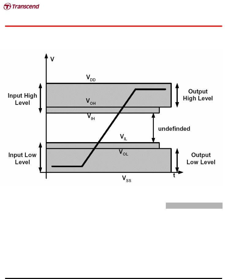
• Bus Signal Levels
As the bus can be supplied with a variable supply voltage, all signal levels are related to the supply voltage.
To meet the requirements of the JEDEC specification JESD8-1A and JESD8-7, the card input and output voltages shall be within the following specified ranges for any VDD of the allowed voltage range:
Parameter |
Symbol |
Min. |
Max. |
Unit |
Remark |
Output HIGH voltage |
VOH |
0.75* VDD |
|
V |
IOH = -100 µA @VDD min |
Output LOW voltage |
VOL |
|
0.125* VDD |
V |
IOL = -100 µA @VDD min |
Input HIGH voltage |
VIH |
0.625* VDD |
VDD + 0.3 |
V |
|
Input LOW voltage |
VIL |
VSS – 0.3 |
0.25* VDD |
V |
|
Transcend Information Inc. |
5 |

SDHC Card series
4~32GB High Capacity Secure Digital Card
• Bus Timing
Parameter |
Symbol |
Min |
Max. |
Unit |
Remark |
Clock CLK (All values are referred to min (VIH) and max (VIL)
|
Clock frequency Data Transfer Mode |
fPP |
0 |
25 |
MHz |
CCARD ≤ 10 pF, (1 card) |
|
|
Clock frequency Identification Mode |
fOD |
0(1)/100 |
400 |
KHz |
CCARD ≤ 10 pF, (1 card) |
|
|
Clock low time |
tWL |
10 |
|
ns |
CCARD ≤ 10 pF, (1 card) |
|
|
Clock high time |
tWH |
10 |
|
ns |
CCARD ≤ 10 pF, (1 card) |
|
|
Clock rise time |
tTLH |
|
10 |
ns |
CCARD ≤ 10 pF, (1 card) |
|
|
Clock fall time |
tTHL |
|
10 |
ns |
CCARD ≤ 10 pF, (1 card) |
|
|
Inputs CMD, DAT (referenced to CLK) |
|
|
|
|
|
|
|
Input set-up time |
tISU |
5 |
|
ns |
CCARD ≤ 10 pF, (1 card) |
|
|
Input hold time |
tIH |
5 |
|
ns |
CCARD ≤ 10 pF, (1 card) |
|
|
Outputs CMD, DAT (referenced to CLK) |
|
|
|
|
|
|
|
|
|
|
|
|
|
|
Transcend Information Inc. |
|
6 |
|
|
|
|
|

SDHC Card series
4~32GB High Capacity Secure Digital Card
Output Delay time during Data Transfer Mode |
tODLY |
0 |
14 |
ns |
CL ≤ 40 pF, (1 card) |
Output Delay time during Identification Mode |
tODLY |
0 |
50 |
ns |
CL ≤ 40 pF, (1 card) |
(1) 0 Hz means to stop the clock. The given minimum frequency range is for cases were continues clock is required
Transcend Information Inc. |
7 |

SDHC Card series
4~32GB High Capacity Secure Digital Card
• Bus Timing (High Speed Mode)
Parameter |
Symbol |
Min |
Max. |
Unit |
Remark |
Clock CLK (All values are referred to min (VIH) and max (VIL)
|
Clock frequency Data Transfer Mode |
fPP |
0 |
50 |
MHz |
CCARD ≤ 10 pF, (1 card) |
|
|
Clock low time |
tWL |
7 |
|
ns |
CCARD ≤ 10 pF, (1 card) |
|
|
Clock high time |
tWH |
7 |
|
ns |
CCARD ≤ 10 pF, (1 card) |
|
|
Clock rise time |
tTLH |
|
3 |
ns |
CCARD ≤ 10 pF, (1 card) |
|
|
Clock fall time |
tTHL |
|
3 |
ns |
CCARD ≤ 10 pF, (1 card) |
|
|
Inputs CMD, DAT (referenced to CLK) |
|
|
|
|
|
|
|
Input set-up time |
tISU |
6 |
|
ns |
CCARD ≤ 10 pF, (1 card) |
|
|
Input hold time |
tIH |
2 |
|
ns |
CCARD ≤ 10 pF, (1 card) |
|
|
Outputs CMD, DAT (referenced to CLK) |
|
|
|
|
|
|
|
|
|
|
|
|
|
|
Transcend Information Inc. |
|
8 |
|
|
|
|
|
 Loading...