


TS16GCF200I
Transcend TS16GCF200I, TS1GCF200I, TS4GCF200I, TS2GCF200I, TS256MCF200I DATASHEET
...
T
T
T
r
r
r
a
a
a
n
n
n
s
s
s
c
c
c
e
e
e
n
n
n
d
d
d
I
I
I
n
n
n
d
d
d
u
u
u
s
s
s
t
t
t
r
r
r
i
i
i
a
a
a
l
l
l
C
C
C
F
F
F
C
C
C
a
a
a
r
r
r
d
d
d
T
T
T
S
S
S
1
1
1
2
2
2
8
8
8
M
M
M
~
~
~
1
1
1
6
6
6
G
G
G
C
C
C
F
F
F
2
2
2
0
0
0
0
0
0
I
I
I
Transcend Information Inc.
V1.2
1
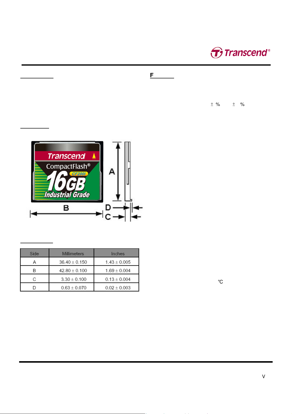
Description
The Transcend CF200I is a High Speed industrial
Compact Flash Card with high quality Flash Memory
assembled on a printed circuit board.
Placement
Dimensions
Features
•
CompactFlash Specification Version 4.1 Compliant
•
RoHS compliant products
•
Single Power Supply: 3.3V
±
5% or 5V
±
10%
•
Operating Temperature: -40
o
C to 85
o
C
•
Storage Temperature: -55
o
C to 100
o
C
•
Humidity (Non condensation): 0% to 95%
•
Built-in 13/24-bit ECC (Error Correction Code)
functionality and wear-leveling algorithm ensures highly
reliable of data transfer
13bit BCH ECC (2k+64 / 4k+128 byte per page flash)
24bit BCH ECC (4k+208 byte per page flash)
•
Operation Modes:
PC Card Memory Mode
PC Card IO Mode
True DE Mode
•
True IDE Mode supports:
Ultra DMA Mode 0 to 5 (UDMA4 as default)
Multi-Word DMA Mode 0 to 4
PIO Mode 0 to 6
•
True IDE Mode: Fixed Disk (Default)
• PC Card Mode: Fixed Disk (Default)
•
Durability of Connector: 10,000 times
• MTBF: 4,000,000 hours (in 25
℃
)
•
Support Global Wear-Leveling, Static Data Refresh,
Early Retirement, and Erase Count Monitor functions to
extend product life
•
Support S.M.A.R.T (Self-defined)
•
Support Security Command
•
Compliant to CompactFlash, PCMCIA, and ATA
standards

T
T
T
r
r
r
a
a
a
n
n
n
s
s
s
c
c
c
e
e
e
n
n
n
d
d
d
I
I
I
n
n
n
d
d
d
u
u
u
s
s
s
t
t
t
r
r
r
i
i
i
a
a
a
l
l
l
C
C
C
F
F
F
C
C
C
a
a
a
r
r
r
d
d
d
T
T
T
S
S
S
1
1
1
2
2
2
8
8
8
M
M
M
~
~
~
1
1
1
6
6
6
G
G
G
C
C
C
F
F
F
2
2
2
0
0
0
0
0
0
I
I
I
Transcend Information Inc.
V1.2
2
Ordering Information
Part Number Interface Transfer Mode Disk Type
True IDE mode
Ultra DMA mode 0~5
(UDMA4 as default)
Multi-Word DMA Mode 0~4
PIO Mode 0 ~ 6
Fixed Disk (Default)
TS128M~16GCF200I
PC Card mode (PCMCIA)
80ns, 100ns, 120ns, 250ns Fixed Disk (Default)
C.H.S Table
Capacity C H S Physical Capacity
128MB 246 16 63 126,959,616 bytes
256MB 493 16 63 254,435,328 bytes
512MB 987 16 63 509,386,752 bytes
1GB 1974 16 63 1,018,773,504 bytes
2GB 3949 16 63 2,038,063,104 bytes
4GB 7899 16 63 4,076,642,304 bytes
8GB 15798 16 63 8,153,284,608 bytes
16GB 16383 15 63 16,039,018,496 bytes
* Note: FAT format for <4GB, FAT32 format for 4~16GB
* Note : 25
℃
, according to CF to IDE connector test on P5K-VM, 1GB RAM * 2, IDE interface support UDMA4,
Windows
®
XP Version 2002 SP2, benchmark utility FDBENCH (version 1.02), copied file 40MB
Performance
Model P/N Read (KB/s) Write (KB/s) Random Read (KB/s)
Random Write (KB/s)
TS128MCF200I 25440 7362 24482 2559
TS256MCF200I 25940 10697 24719 3513
TS512MCF200I 25940 10317 24482 3390
TS1GCF200I 29111 12363 27563 4121
TS2GCF200I
28804 20791 27288 5079
TS4GCF200I 28784 22200 26736 6635
TS8GCF200I 49349 36900 44425 11966
TS16GCF200I 50381 39689 46757 10739
T
T
T
r
r
r
a
a
a
n
n
n
s
s
s
c
c
c
e
e
e
n
n
n
d
d
d
I
I
I
n
n
n
d
d
d
u
u
u
s
s
s
t
t
t
r
r
r
i
i
i
a
a
a
l
l
l
C
C
C
F
F
F
C
C
C
a
a
a
r
r
r
d
d
d
T
T
T
S
S
S
1
1
1
2
2
2
8
8
8
M
M
M
~
~
~
1
1
1
6
6
6
G
G
G
C
C
C
F
F
F
2
2
2
0
0
0
0
0
0
I
I
I
Transcend Information Inc.
V1.2
3
1. Read/Write operation is drived by IOMeter with 10MB file each operation.
2. StandBy Current : 5V : 2.8mA 3.3V : 2.2mA
3. All data above are maximum value of each measurements.
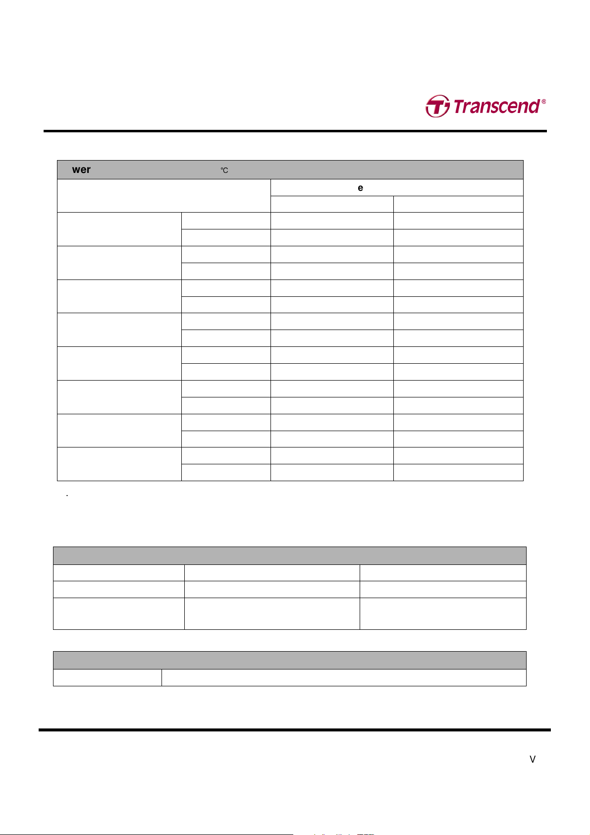
Power Requirements
(DC 5V
@
25
℃
)
Power Consumption (mA)
Part Number & Input Voltage
Read Write
3.3V ± 10%
61 52.6
TS128MCF200I
5V
±
10%
102.6 53.4
3.3V
±
10%
61.3 57.6
TS256MCF200I
5V
±
10%
99 58.8
3.3V
±
10%
86.9 57.8
TS512MCF200I
5V
±
10%
64.1 59.3
3.3V
±
10%
67.5 65.9
TS1GCF200I
5V ± 10%
71.3 68.6
3.3V ± 10%
71 89.6
TS2GCF200I
5V
±
10%
116 93.1
3.3V
±
10%
69.6 89.2
TS4GCF200I
5V
±
10%
113.8 98.9
3.3V
±
10%
88.6 137.1
TS8GCF200I
5V
±
10%
99.9 139.9
3.3V ± 10%
139.5 143.4
TS16GCF200I
5V ± 10%
173.4 152.6
SHOCK & Vibration Test
Condition Standard
Mechanical Shock Test
1500G, 0.5ms, 3 axes IEC 60068-2-27
Vibration Test
20G (Peak-to-Peak)
20Hz to 2000Hz (Frequency)
IEC 60068-2-6
Regulations
Compliance
CE, FCC and BSMI

T
T
T
r
r
r
a
a
a
n
n
n
s
s
s
c
c
c
e
e
e
n
n
n
d
d
d
I
I
I
n
n
n
d
d
d
u
u
u
s
s
s
t
t
t
r
r
r
i
i
i
a
a
a
l
l
l
C
C
C
F
F
F
C
C
C
a
a
a
r
r
r
d
d
d
T
T
T
S
S
S
1
1
1
2
2
2
8
8
8
M
M
M
~
~
~
1
1
1
6
6
6
G
G
G
C
C
C
F
F
F
2
2
2
0
0
0
0
0
0
I
I
I
Transcend Information Inc.
V1.2
4
More Functions to extend product life
1. Global Wear Leveling – Advanced algorithm to enhance the Wear-Leveling Efficiency
There are 3 main processes in global wear leveling approaches:
(1) Record the block erase count and save in the wear-leveling table.
(2) Find the static-block and save it in wear-leveling pointer.
(3) Check the erase count when the block popped from spare pool. If the
block erase count is bigger
than WEARCNT, then swapped the static-block and over-count-block.
After actual test, global wear leveling successfully even the erase
count of every block; hence, it can
extend the life expectancy of Flash product.
2. StaticDataRefresh Technology – Keeping Data Healthy
There are many variants that would disturb the charge inside a Flash cell. These variants can be:
time,
read operations, undesired charge, heat, etc; each variant would create a charge loss,
and the contents
shift in their charge levels slightly. In our everyday usage –
more than 60% are repeated read operations,
the accumulated charge loss would eventually result in the data loss.
Normally, ECC engine corrections are taken place without affecting the host normal
operations. As
time passes by, the number of error bits accumulated in the read transaction
exceeds the correcting
capability of the ECC engine, resulting in corrupted data being sent to the host.
To prevent this, Transcend’s CF200I monitor the error bit levels at each read
operation; when it
reaches the preset threshold value, the controller automatically performs
data refresh to “restore” the
correct charge levels in the cell. This implementation practically restores the data to its original, error-fr
ee
state, and hence, lengthening the life of the data.
3. EarlyRetirement – Avoiding Data Loss Due to Weak Block
The StaticDataRefresh feature functions well when the cells in a block are still healthy. As
the block
ages over time, it cannot store charge reliably anymore, EarlyRetirement enters the scene.
EarlyRetirement works by moving the static data to another block (a health block) before
the previously
used block becomes completely incapable of holding charges for data. W hen the charge loss error leve
l
exceeds another threshold value (higher from that for
StaticDataRefresh), the controller automatically
moves its data to another block. In addition,
the original block is then marked as a bad block, which
prevents its further use, and thus the block enters the state of “EarlyRetirement.”
Note that, through this
process, the incorrect data are detected and effectively corrected by
the ECC engine, thus the data in the
new block is stored error-free.
T
T
T
r
r
r
a
a
a
n
n
n
s
s
s
c
c
c
e
e
e
n
n
n
d
d
d
I
I
I
n
n
n
d
d
d
u
u
u
s
s
s
t
t
t
r
r
r
i
i
i
a
a
a
l
l
l
C
C
C
F
F
F
C
C
C
a
a
a
r
r
r
d
d
d
T
T
T
S
S
S
1
1
1
2
2
2
8
8
8
M
M
M
~
~
~
1
1
1
6
6
6
G
G
G
C
C
C
F
F
F
2
2
2
0
0
0
0
0
0
I
I
I
Transcend Information Inc.
V1.2
5
Transcend

T
T
T
r
r
r
a
a
a
n
n
n
s
s
s
c
c
c
e
e
e
n
n
n
d
d
d
I
I
I
n
n
n
d
d
d
u
u
u
s
s
s
t
t
t
r
r
r
i
i
i
a
a
a
l
l
l
C
C
C
F
F
F
C
C
C
a
a
a
r
r
r
d
d
d
T
T
T
S
S
S
1
1
1
2
2
2
8
8
8
M
M
M
~
~
~
1
1
1
6
6
6
G
G
G
C
C
C
F
F
F
2
2
2
0
0
0
0
0
0
I
I
I
Transcend Information Inc.
V1.2
6
Block Diagram

T
T
T
r
r
r
a
a
a
n
n
n
s
s
s
c
c
c
e
e
e
n
n
n
d
d
d
I
I
I
n
n
n
d
d
d
u
u
u
s
s
s
t
t
t
r
r
r
i
i
i
a
a
a
l
l
l
C
C
C
F
F
F
C
C
C
a
a
a
r
r
r
d
d
d
T
T
T
S
S
S
1
1
1
2
2
2
8
8
8
M
M
M
~
~
~
1
1
1
6
6
6
G
G
G
C
C
C
F
F
F
2
2
2
0
0
0
0
0
0
I
I
I
Transcend Information Inc.
V1.2
7
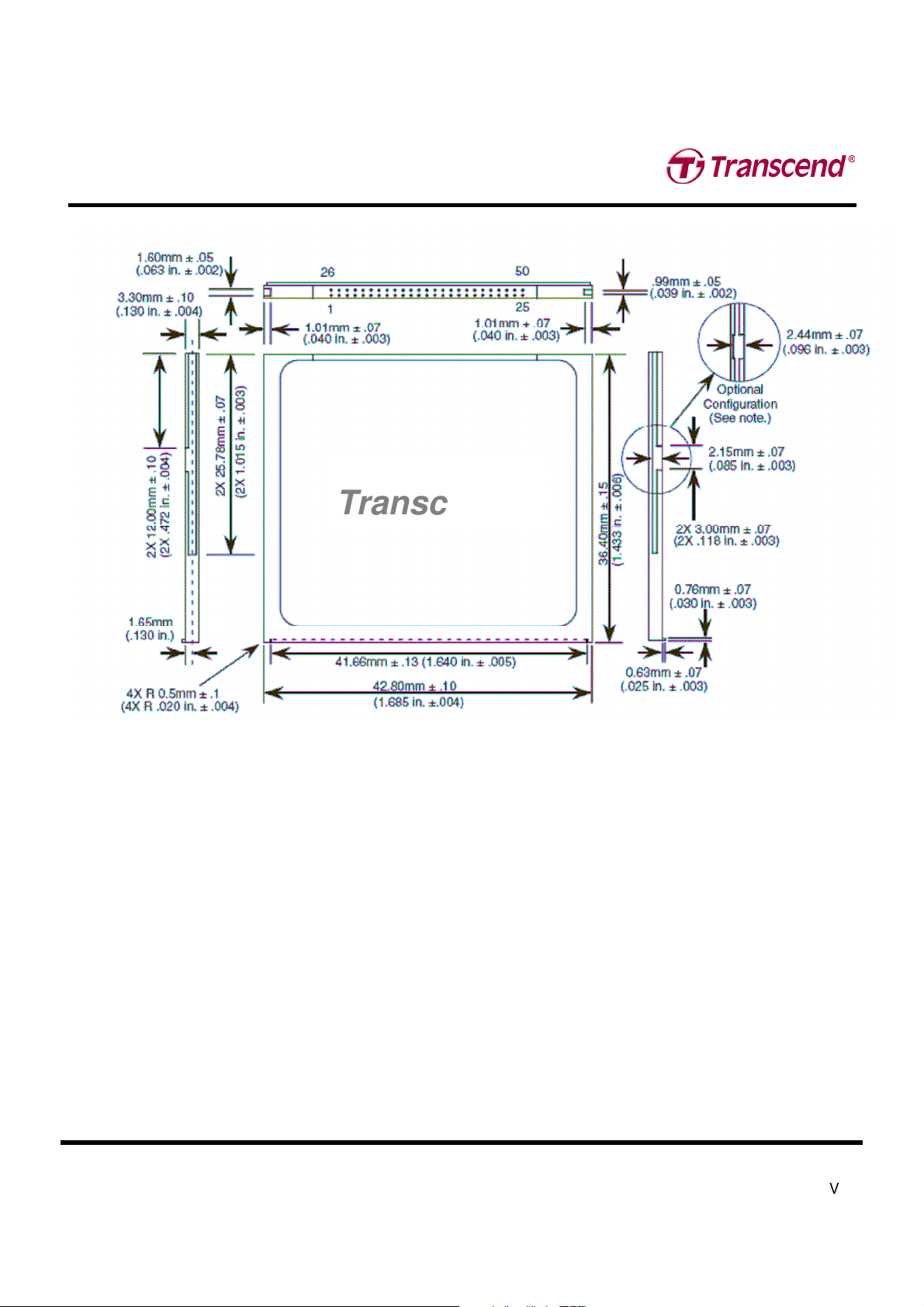
Pin Assignments and Pin Type
T
T
T
r
r
r
a
a
a
n
n
n
s
s
s
c
c
c
e
e
e
n
n
n
d
d
d
I
I
I
n
n
n
d
d
d
u
u
u
s
s
s
t
t
t
r
r
r
i
i
i
a
a
a
l
l
l
C
C
C
F
F
F
C
C
C
a
a
a
r
r
r
d
d
d
T
T
T
S
S
S
1
1
1
2
2
2
8
8
8
M
M
M
~
~
~
1
1
1
6
6
6
G
G
G
C
C
C
F
F
F
2
2
2
0
0
0
0
0
0
I
I
I
Transcend Information Inc.
V1.2
8
Note: 1) These signals are required only for 16 bit accesses and not required when installed in 8 bit
systems. Devices should allow for 3-state signals not to consume current.
2) The signal should be grounded by the host.
3) The signal should be tied to VCC by the host.
4) The mode is required for CompactFlash Storage Cards.
5) The -CSEL signal is ignored by the card in PC Card modes. However, because it is not
pulled upon the card in these modes, it should not be left floating by the host in PC Card
modes. In these modes, the pin should be connected by the host to PC Card A25 or
grounded by the host.
6) If DMA operations are not used, the signal should be held high or tied to VCC by the host. For
proper operation in older hosts: while DMA operations are not active, the card shall ignore
this signal,including a floating condition
7) Signal usage in True IDE Mode except when Ultra DMA mode protocol is active.
8) Signal usage in True IDE Mode when Ultra DMA mode protocol DMA Write is active.
9) Signal usage in True IDE Mode when Ultra DMA mode protocol DMA Read is active.
10) Signal usage in PC Card I/O and Memory Mode when Ultra DMA mode protocol DMA Write is active.
11) Signal usage in PC Card I/O and Memory Mode when Ultra DMA mode protocol DMA Read is active.
12) Signal usage in PC Card I/O and Memory Mode when Ultra DMA protocol is active.

T
T
T
r
r
r
a
a
a
n
n
n
s
s
s
c
c
c
e
e
e
n
n
n
d
d
d
I
I
I
n
n
n
d
d
d
u
u
u
s
s
s
t
t
t
r
r
r
i
i
i
a
a
a
l
l
l
C
C
C
F
F
F
C
C
C
a
a
a
r
r
r
d
d
d
T
T
T
S
S
S
1
1
1
2
2
2
8
8
8
M
M
M
~
~
~
1
1
1
6
6
6
G
G
G
C
C
C
F
F
F
2
2
2
0
0
0
0
0
0
I
I
I
Transcend Information Inc.
V1.2
9
Signal Description
Signal Name
Dir.
Pin
Description
A10 – A00
(PC Card Memory Mode)
A10 – A00
(PC Card I/O Mode)
A02 - A00
(True IDE Mode)
I
I
8,10,11,12,
14,15,16,17,
18,19,20
18,19,20
These address lines along with the -REG signal are used to
select the following:
The I/O port address registers within the CompactFlash Storage Card , the
memory mapped
port address registers within the CompactFlash Storage Card,
a byte in the card's information structure and its
configuration control and status
registers.
This signal is the same as the PC Card Memory Mode signal.
In True IDE Mode, only A[02:00] are used to select the one of eight registers
in the Task File, the remaining address lines should be grounded by the
host.
BVD1
(PC Card Memory Mode)
-STSCHG
(PC Card I/O Mode)
Status Changed
-PDIAG
(True IDE Mode)
I/O
46
This signal is asserted high, as BVD1 is not supported.
This signal is asserted low to alert the host to changes in the
READY and Write
Protect states, while the I/O interface is configured. Its use is controlled by the
Card Config and Status Register.
In the True IDE Mode, this input / output is the Pass Diagnostic signal in the
Master / Slave handshake protocol.
BVD2
(PC Card Memory Mode)
-SPKR
(PC Card I/O Mode)
-DASP
(True IDE Mode)
I/O
45
This signal is asserted high, as BVD2 is not supported.
This line is the Binary Audio output from the card. If the Card does not support
the Binary Audio function, this line should be held negated.
In the True IDE Mode, this input/output is the Disk Active/Slave
Present signal in
the Master/Slave handshake protocol.
-CD1, -CD2
(PC Card Memory Mode)
-CD1, -CD2
(PC Card I/O Mode)
-CD1, -CD2
(True IDE Mode)
O
26,25
These Card Detect pins are connected to ground on the
CompactFlash Storage
Card. They are used by the host to determine that the CompactFlash Storage
Card is fully inserted into its socket.
This signal is the same for all modes.
This signal is the same for all modes.

T
T
T
r
r
r
a
a
a
n
n
n
s
s
s
c
c
c
e
e
e
n
n
n
d
d
d
I
I
I
n
n
n
d
d
d
u
u
u
s
s
s
t
t
t
r
r
r
i
i
i
a
a
a
l
l
l
C
C
C
F
F
F
C
C
C
a
a
a
r
r
r
d
d
d
T
T
T
S
S
S
1
1
1
2
2
2
8
8
8
M
M
M
~
~
~
1
1
1
6
6
6
G
G
G
C
C
C
F
F
F
2
2
2
0
0
0
0
0
0
I
I
I
Transcend Information Inc.
V1.2
10
Signal Name
Dir.
Pin
Description
-CE1, -CE2
(PC Card Memory Mode)
Card Enable
-CE1, -CE2
(PC Card I/O Mode)
Card Enable
-CS0, -CS1
(True IDE Mode)
I
7,32
These input signals are used both to select the card and to
indicate to the card
whether a byte or a word operation is being performed. -CE2 always accesses
the odd byte of the word.-CE1 accesses the even byte or the Odd byte of the
word depending on A0 and -CE2. A multiplexing scheme based on A0,-CE1,
-CE2 allows 8 bit hosts to access all data on D0-D7. See Table 27, Table 29,
Table 31, Table 35, Table 36 and Table 37.
This signal is the same as the PC Card Memory Mode signal.
In the True IDE Mode, -CS0 is the address range select for the task file
registers while -CS1 is used to select the Alternate Status Register and the
Device Control Register.
While –DMACK is asserted, -CS0 and –CS1 shall be held negated and the
width of the transfers shall be 16 bits.
-CSEL
(PC Card Memory Mode)
-CSEL
(PC Card I/O Mode)
-CSEL
(True IDE Mode)
I
39
This signal is not used for this mode, but should be connected by
the host to PC
Card A25 or grounded by the host.
This signal is not used for this mode, but should be connected by
the host to PC
Card A25 or grounded by the host.
This internally pulled up signal is used to configure this device as
a Master or a
Slave when configured in the True IDE Mode.
When this pin is grounded, this device is configured as a Master.
When the pin is open, this device is configured as a Slave.
D15 - D00
(PC Card Memory Mode)
D15 - D00
(PC Card I/O Mode)
D15 - D00
(True IDE Mode)
I/O
31,30,29,28,
27,49,48,47,
6,5,4,3,2,
23, 22, 21
These lines carry the Data, Commands and Status information
between the host
and the controller. D00 is the LSB of the Even
Byte of the Word. D08 is the LSB
of the Odd Byte of the Word.
This signal is the same as the PC Card Memory Mode signal.
In True IDE Mode, all Task File operations occur in byte mode
on the low order
bus D[7:0] while all data transfers are 16 bit using D[15:0].
GND
(PC Card Memory Mode)
GND
(PC Card I/O Mode)
GND
(True IDE Mode)
--
1,50
Ground.
This signal is the same for all modes.
This signal is the same for all modes.

T
T
T
r
r
r
a
a
a
n
n
n
s
s
s
c
c
c
e
e
e
n
n
n
d
d
d
I
I
I
n
n
n
d
d
d
u
u
u
s
s
s
t
t
t
r
r
r
i
i
i
a
a
a
l
l
l
C
C
C
F
F
F
C
C
C
a
a
a
r
r
r
d
d
d
T
T
T
S
S
S
1
1
1
2
2
2
8
8
8
M
M
M
~
~
~
1
1
1
6
6
6
G
G
G
C
C
C
F
F
F
2
2
2
0
0
0
0
0
0
I
I
I
Transcend Information Inc.
V1.2
11
Signal Name
Dir.
Pin
Description
-INPACK
(PC Card Memory Mode)
-INPACK
(PC Card I/O Mode)
Input Acknowledge
DMARQ
(True IDE Mode)
O
43 This signal is not used in this mode.
The Input Acknowledge signal is asserted by the CompactFlash Storage Card
when the card is selected and responding to an I/O read cycle at the address
that is on the address bus. This signal is used by the host to control the enable
of
any input data buffers between the CompactFlash Storage Card and the CPU.
This signal is a DMA Request that is used for DMA data
transfers between host
and device. It shall be asserted by the
device when it is ready to transfer data to
or from the host. For Multiword DMA transfers, the direction of data transfer is
controlled by -IORD and -IOWR. This signal is used in a
handshake manner with
-DMACK, i.e., the device shall wait until the host asserts -DMACK before
negating DMARQ, and reasserting DMARQ if there is more data to transfer.
DMARQ shall not be driven when the device is not selected.
While a DMA operation is in progress, -CS0 and –CS1 shall be held negated
and the width of the transfers shall be 16 bits.
If there is no hardware support for DMA mode in the host, this
output signal is not
used and should not be connected at the host. In this case,
the BIOS must report
that DMA mode is not supported by the host so that device drivers will not
attempt DMA mode.
A host that does not support DMA mode and implements both PCMCIA and
True-IDE modes of operation need not alter the PCMCIA mode connections
while in True-IDE mode as long as
this does not prevent proper operation in any
mode.
-IORD
(PC Card Memory Mode)
-IORD
(PC Card I/O Mode)
-IORD
(True IDE Mode – Except
Ultra DMA Protocol Active)
-HDMARDY
(True IDE Mode – In Ultra
DMA Protocol DMA Read)
HSTROBE
(True IDE Mode – In Ultra
DMA Protocol DMA Write)
I
34 This signal is not used in this mode.
This is an I/O Read strobe generated by the host. This signal
gates I/O data onto
the bus from the CompactFlash Storage Card when the card is configu
red to use
the I/O interface.
In True IDE Mode, while Ultra DMA mode is not active, this
signal has the same
function as in PC Card I/O Mode.
In True IDE Mode when Ultra DMA mode DMA Read is active, this signal is
asserted by the host to indicate that the host is read to receive Ultra DMA data-
in
bursts. The host may negate -HDMARDY to pause an Ultra DMA transfer.
In True IDE Mode when Ultra DMA mode DMA Write is active,
this signal is the
data out strobe generated by the host. Both the rising and falling edge of
HSTROBE cause data to be latched by the device. The host may stop
generating HSTROBE edges to pause an Ultra DMA data-out burst.

T
T
T
r
r
r
a
a
a
n
n
n
s
s
s
c
c
c
e
e
e
n
n
n
d
d
d
I
I
I
n
n
n
d
d
d
u
u
u
s
s
s
t
t
t
r
r
r
i
i
i
a
a
a
l
l
l
C
C
C
F
F
F
C
C
C
a
a
a
r
r
r
d
d
d
T
T
T
S
S
S
1
1
1
2
2
2
8
8
8
M
M
M
~
~
~
1
1
1
6
6
6
G
G
G
C
C
C
F
F
F
2
2
2
0
0
0
0
0
0
I
I
I
Transcend Information Inc.
V1.2
12
Signal Name
Dir.
Pin
Description
-IOWR
(PC Card Memory Mode)
-IOWR
(PC Card I/O Mode)
-IOWR
(True IDE Mode – Except
Ultra DMA Protocol Active)
STOP
(True IDE Mode – Ultra DMA
Protocol Active)
I
35
This signal is not used in this mode.
The I/O Write strobe pulse is used to clock I/O data on the Card Data bus into
the CompactFlash Storage Card controller registers when the CompactFlash
Storage Card is configured to use the I/O interface.
The clocking shall occur on the negative to positive edge of the signal (trailing
edge).
In True IDE Mode, while Ultra DMA mode protocol is not active, this signal has
the same function as in PC Card I/O Mode. When Ultra DMA mode protocol is
supported, this signal must be negated before entering Ultra DMA mode
protocol.
In True IDE Mode, while Ultra DMA mode protocol is active, the
assertion of this
signal causes the termination of the Ultra DMA burst.
-OE
(PC Card Memory Mode)
-OE
(PC Card I/O Mode)
-ATA SEL
(True IDE Mode)
I
9
This is an Output Enable strobe generated by the host interface. It is used to
read data from the CompactFlash Storage Card in Memory Mode and to read
the CIS and configuration registers.
In PC Card I/O Mode, this signal is used to read the CIS and configuration
registers.
To enable True IDE Mode this input should be grounded by the host.
READY
(PC Card Memory Mode)
-IREQ
(PC Card I/O Mode)
INTRQ
(True IDE Mode)
O
37
In Memory Mode, this signal is set high when the CompactFlash Storage Card
is ready to accept a new data transfer
operation and is held low when the card is
busy.
At power up and at Reset, the READY signal is held low (busy) until the
CompactFlash Storage Card has completed its power up or reset function. No
access of any type should be made to the CompactFlash Storage Card during
this time.
Note, however, that when a card is powered up and used with RESET
continuously disconnected or asserted, the Reset function of the RESET pin is
disabled. Consequently, the continuous assertion of RESET from the
application of power
shall not cause the READY signal to remain continuously in
the busy state.
I/O Operation – After the CompactFlash Storage Card Card has been
configured for I/O operation, this signal is used as -
Interrupt Request. This line is
strobed low to generate a pulse mode interrupt or held low for a level mode
interrupt.
In True IDE Mode signal is the active high Interrupt Request to the host.

T
T
T
r
r
r
a
a
a
n
n
n
s
s
s
c
c
c
e
e
e
n
n
n
d
d
d
I
I
I
n
n
n
d
d
d
u
u
u
s
s
s
t
t
t
r
r
r
i
i
i
a
a
a
l
l
l
C
C
C
F
F
F
C
C
C
a
a
a
r
r
r
d
d
d
T
T
T
S
S
S
1
1
1
2
2
2
8
8
8
M
M
M
~
~
~
1
1
1
6
6
6
G
G
G
C
C
C
F
F
F
2
2
2
0
0
0
0
0
0
I
I
I
Transcend Information Inc.
V1.2
13
Signal Name
Dir.
Pin
Description
-REG
(PC Card Memory Mode)
Attribute Memory Select
-REG
(PC Card I/O Mode)
I
44
This signal is used during Memory Cycles to distinguish between Common
Memory and Register (Attribute) Memory accesses.
High for Common Memory,
Low for Attribute Memory.
The signal shall also be active (low) during I/O Cycles when the I/O address is
on the Bus.
-DMACK
(True IDE Mode)
This is a DMA Acknowledge signal that is asserted by the host in response to
DMARQ to initiate DMA transfers.
While DMA operations are not active, the card shall ignore the -
DMACK signal,
including a floating condition.
If DMA operation is not supported by a True IDE Mode only host, this signal
should be driven high or connected to VCC by the host.
A host that does not support DMA mode and implements both PCMCIA and
True-IDE modes of operation need not alter the PCMCIA mode connections
while in True-IDE mode as long as this does not prevent proper operation all
modes.
RESET
(PC Card Memory Mode)
RESET
(PC Card I/O Mode)
-RESET
(True IDE Mode)
I
41 The CompactFlash Storage Card is Reset when the
RESET pin is high with the
following important exception:
The host may leave the RESET pin open or keep it continually high from the
application of power without causing a continuous Reset of the card. Under
either of these conditions, the card shall emerge from power-up having
completed an initial Reset.
The CompactFlash Storage Card is also Reset when the Soft Reset bit in the
Card Configuration Option Register is set.
This signal is the same as the PC Card Memory Mode signal.
In the True IDE Mode, this input pin is the active low hardware reset from the
host.
VCC
(PC Card Memory Mode)
VCC
(PC Card I/O Mode)
VCC
(True IDE Mode)
--
13,38 +5 V, +3.3 V power.
This signal is the same for all modes.
This signal is the same for all modes.

T
T
T
r
r
r
a
a
a
n
n
n
s
s
s
c
c
c
e
e
e
n
n
n
d
d
d
I
I
I
n
n
n
d
d
d
u
u
u
s
s
s
t
t
t
r
r
r
i
i
i
a
a
a
l
l
l
C
C
C
F
F
F
C
C
C
a
a
a
r
r
r
d
d
d
T
T
T
S
S
S
1
1
1
2
2
2
8
8
8
M
M
M
~
~
~
1
1
1
6
6
6
G
G
G
C
C
C
F
F
F
2
2
2
0
0
0
0
0
0
I
I
I
Transcend Information Inc.
V1.2
14
Signal Name
Dir.
Pin
Description
-VS1
-VS2
(PC Card Memory Mode)
-VS1
-VS2
(PC Card I/O Mode)
-VS1
-VS2
(True IDE Mode)
O
33
40
Voltage Sense Signals. -VS1 is grounded on the Card and sensed by the Host
so that the CompactFlash Storage Card CIS can be read at 3.3 volts and -
VS2 is
reserved by PCMCIA for a secondary voltage and is not connected on the Card.
This signal is the same for all modes.
This signal is the same for all modes.
-WAIT
(PC Card Memory Mode)
-WAIT
(PC Card I/O Mode)
IORDY
(True IDE Mode – Except
Ultra DMA Mode)
-DDMARDY
(True IDE Mode – Ultra DMA
Write Mode)
DSTROBE
(True IDE Mode – Ultra
DMA Read Mode)
O
42 The -WAIT signal is driven low by the CompactFlash Storage
Card to signal the
host to delay completion of a memory or I/O cycle that is in progress.
This signal is the same as the PC Card Memory Mode signal.
In True IDE Mode, except in Ultra DMA modes, this output signal may be used
as IORDY.
In True IDE Mode, when Ultra DMA mode DMA Write is active, this signal is
asserted by the host to indicate that the device is read to receive Ultra DMA
data-in bursts. The device may negate -DDMARDY to pause an Ultra DMA
transfer.
In True IDE Mode, when Ultra DMA mode DMA Write is active,
this signal is the
data out strobe generated by the device. Both the rising and falling edge of
DSTROBE cause data to be latched by the host. The device may stop
generating DSTROBE edges to pause an Ultra DMA data-out burst.
-WE
(PC Card Memory Mode)
-WE
(PC Card I/O Mode)
-WE
(True IDE Mode)
I
36 This is a signal driven by the host and used for strobing memory
write data to the
registers of the CompactFlash Storage Card w
hen the card is configured in the
memory interface mode. It is also used for writing the configuration registers.
In PC Card I/O Mode, this signal is used for writing the configuration registers.
In True IDE Mode, this input signal is not used and should be
connected to VCC
by the host.
WP
(PC Card Memory Mode)
Write Protect
-IOIS16
(PC Card I/O Mode)
-IOCS16
(True IDE Mode)
O
24
Memory Mode – The CompactFlash Storage Card
does not have a write protect
switch. This signal is held low after the completion of the reset initialization
sequence.
I/O Operation – When the CompactFlash Storage Card is configured for I/O
Operation Pin 24 is used for the -I/O Selected is 16 Bit Port (-
IOIS16) function. A
Low signal indicates that a 16 bit or odd byte only o
peration can be performed at
the addressed port.
In True IDE Mode this output signal is asserted low when this
device is expecting
a word data transfer cycle.

T
T
T
r
r
r
a
a
a
n
n
n
s
s
s
c
c
c
e
e
e
n
n
n
d
d
d
I
I
I
n
n
n
d
d
d
u
u
u
s
s
s
t
t
t
r
r
r
i
i
i
a
a
a
l
l
l
C
C
C
F
F
F
C
C
C
a
a
a
r
r
r
d
d
d
T
T
T
S
S
S
1
1
1
2
2
2
8
8
8
M
M
M
~
~
~
1
1
1
6
6
6
G
G
G
C
C
C
F
F
F
2
2
2
0
0
0
0
0
0
I
I
I
Transcend Information Inc.
V1.2
15
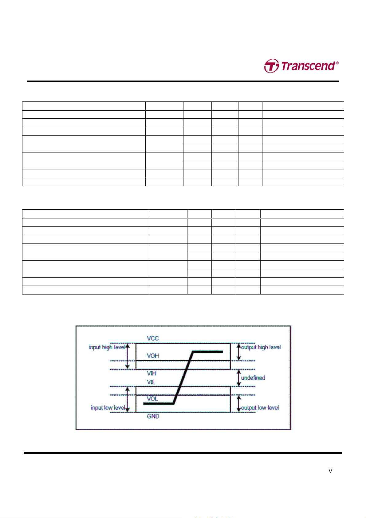
Electrical Specification
The following tables indicate all D.C. Characteristics for the CompactFlash Storage Card. Unless
otherwise stated, conditions are:
Vcc = 5V ±10%
Vcc = 3.3V ± 5%
Absolute Maximum Conditions
Input Power
Input Leakage Current
Input Characteristics
CompactFlash interface I/O at 5.0V
Parameter Symbol Min. Max. Unit Remark
Supply Voltage V
CC
4.5 5.5 V
High level output voltage V
OH
V
CC
-0.8
V
Low level output voltage V
OL
0.8 V
4.0 V Non-schmitt trigger
High level input voltage V
IH
2.92 V Schmitt trigger
1
0.8 V Non-schmitt trigger
Low level input voltage V
IL
1.70 V Schmitt trigger
1
Pull up resistance
2
R
PU
50. 73 kOhm
Pull down resistance R
PD
50 97 kOhm
T
T
T
r
r
r
a
a
a
n
n
n
s
s
s
c
c
c
e
e
e
n
n
n
d
d
d
I
I
I
n
n
n
d
d
d
u
u
u
s
s
s
t
t
t
r
r
r
i
i
i
a
a
a
l
l
l
C
C
C
F
F
F
C
C
C
a
a
a
r
r
r
d
d
d
T
T
T
S
S
S
1
1
1
2
2
2
8
8
8
M
M
M
~
~
~
1
1
1
6
6
6
G
G
G
C
C
C
F
F
F
2
2
2
0
0
0
0
0
0
I
I
I
Transcend Information Inc.
V1.2
16
CompactFlash interface I/O at 3.3V
Parameter Symbol Min. Max. Unit Remark
Supply Voltage V
CC
2.97 3.63 V
High level output voltage V
OH
V
CC
-0.8
V
Low level output voltage V
OL
0.8 V
2.4 V Non-schmitt trigger
High level input voltage V
IH
2.05 V Schmitt trigger
1
0.6 V Non-schmitt trigger
Low level input voltage V
IL
1.25 V Schmitt trigger
1
Pull up resistance
2
R
PU
52.7 141 kOhm
Pull down resistance R
PD
47.5 172 kOhm
The I/O pins other than CompactFlash interface
Parameter Symbol Min. Max. Unit Remark
Supply Voltage V
CC
2.7 3.6 V
High level output voltage V
OH
2.4 V
Low level output voltage V
OL
0.4 V
2.0 V Non-schmitt trigger
High level input voltage V
IH
1.4 2.0 V Schmitt trigger
0.8 V Non-schmitt trigger
Low level input voltage V
IL
0.8 1.2 V Schmitt trigger
Pull up resistance R
PU
40 kOhm
Pull down resistance R
PD
40 kOhm
1. Include CE1, CE2, HREG, HOE. HIOE, HWE, HIOW pins.
2. Include CE1, CE2, HREG, HOE. HIOE, HWE, HIOW, CSEL, PDIAG, DASP pins.
T
T
T
r
r
r
a
a
a
n
n
n
s
s
s
c
c
c
e
e
e
n
n
n
d
d
d
I
I
I
n
n
n
d
d
d
u
u
u
s
s
s
t
t
t
r
r
r
i
i
i
a
a
a
l
l
l
C
C
C
F
F
F
C
C
C
a
a
a
r
r
r
d
d
d
T
T
T
S
S
S
1
1
1
2
2
2
8
8
8
M
M
M
~
~
~
1
1
1
6
6
6
G
G
G
C
C
C
F
F
F
2
2
2
0
0
0
0
0
0
I
I
I
Transcend Information Inc.
V1.2
17
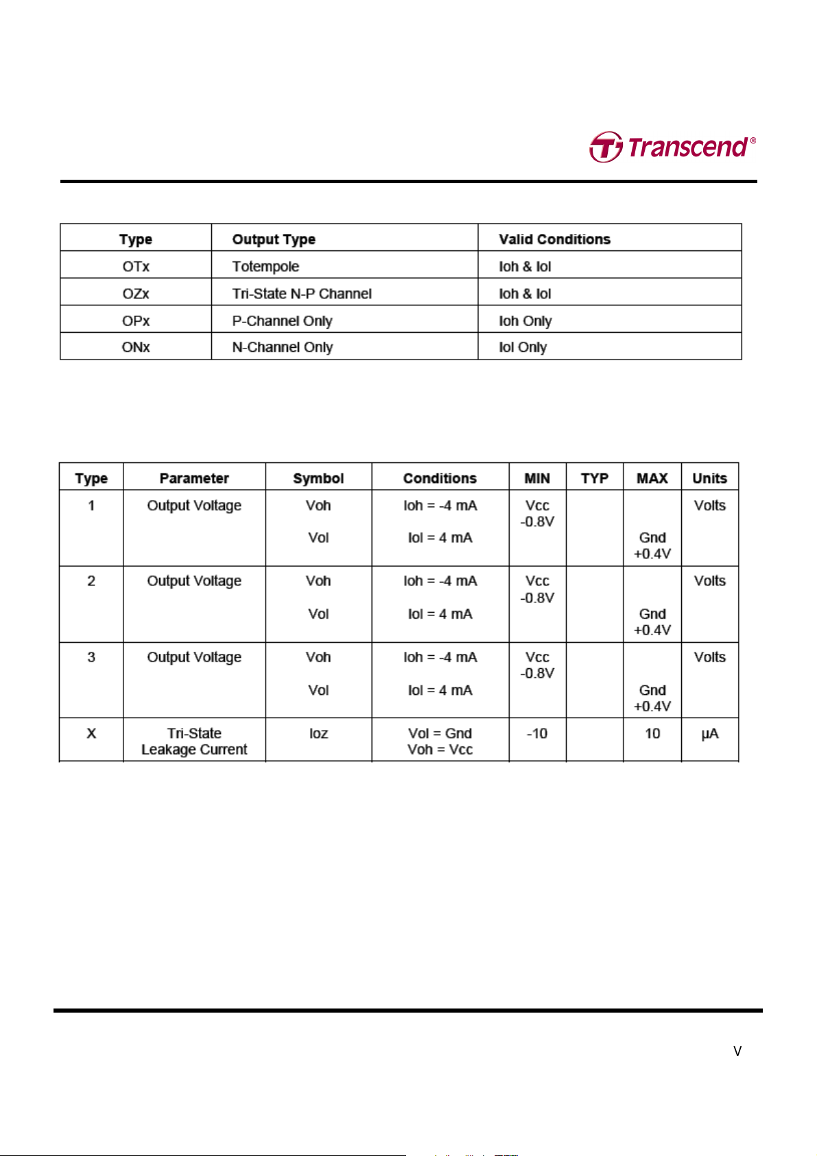
Output Drive Type
Output Drive Characteristics
T
T
T
r
r
r
a
a
a
n
n
n
s
s
s
c
c
c
e
e
e
n
n
n
d
d
d
I
I
I
n
n
n
d
d
d
u
u
u
s
s
s
t
t
t
r
r
r
i
i
i
a
a
a
l
l
l
C
C
C
F
F
F
C
C
C
a
a
a
r
r
r
d
d
d
T
T
T
S
S
S
1
1
1
2
2
2
8
8
8
M
M
M
~
~
~
1
1
1
6
6
6
G
G
G
C
C
C
F
F
F
2
2
2
0
0
0
0
0
0
I
I
I
Transcend Information Inc.
V1.2
18
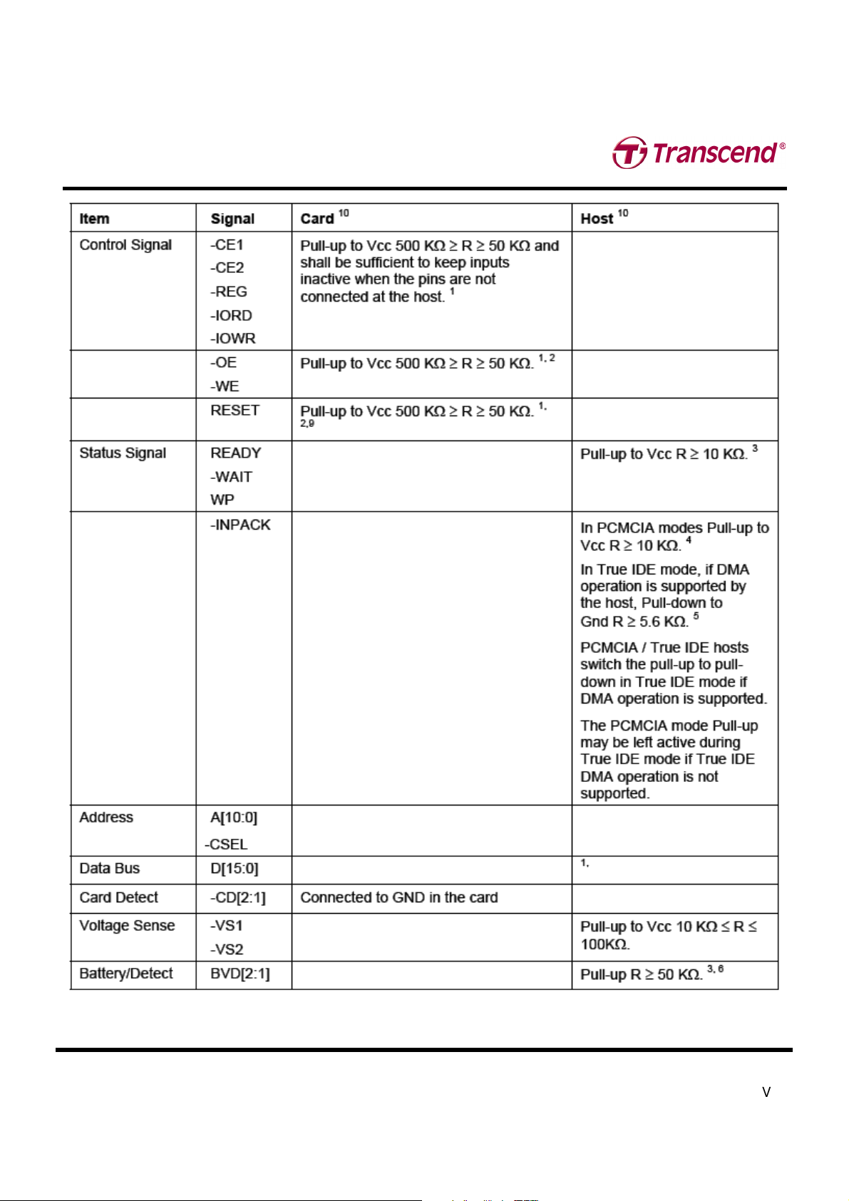
Signal Interface

T
T
T
r
r
r
a
a
a
n
n
n
s
s
s
c
c
c
e
e
e
n
n
n
d
d
d
I
I
I
n
n
n
d
d
d
u
u
u
s
s
s
t
t
t
r
r
r
i
i
i
a
a
a
l
l
l
C
C
C
F
F
F
C
C
C
a
a
a
r
r
r
d
d
d
T
T
T
S
S
S
1
1
1
2
2
2
8
8
8
M
M
M
~
~
~
1
1
1
6
6
6
G
G
G
C
C
C
F
F
F
2
2
2
0
0
0
0
0
0
I
I
I
Transcend Information Inc.
V1.2
19
Notes: 1) Control Signals: each card shall present a load to the socket no larger than 50 pF
10
at a DC current of 700
μ
A
low state and 150
μ
A high state, including pull-resistor. The socket shall be able to drive at least the following
load
10
while meeting all AC timing requirements: (the number of sockets wired in parallel) multiplied by (50 pF
with DC current 700
μ
A low state and 150
μ
A high state per socket).
2) Resistor is optional.
3) Status Signals: the socket shall present a load to the card no larger than 50 pF
10
at a DC current of 400
μ
A low
state and 100
μ
A high state, including pull-up resistor. The card shall be able to drive at least the following load
10
while meeting all AC timing requirements: 50 pF at a DC current of 400
μ
A low state and 100
μ
A high state.
4) Status Signals: the socket shall present a load to the card no larger than 50 pF
10
at a DC current of 400
μ
A low
state and 100
μ
A high state, including pull-up resistor. The card shall be able to drive at least the following load
10
while meeting all AC timing requirements: 50 pF at a DC current of 400
μ
A low state and 100
μ
A high state.
5) Status Signals: the socket shall present a load to the card no larger than 50 pF
10
at a DC current of 400
μ
A low
state and 100
μ
A high state, including pull-up resistor. The card shall be able to drive at least the following load
10
while meeting all AC timing requirements: 50 pF at a DC current of 400
μ
A low state and 1100
μ
A high state.
6) BVD2 was not defined in the JEIDA 3.0 release. Systems fully supporting JEIDA release 3 SRAM cards shall
pull-up pin 45 (BVD2) to avoid sensing their batteries as “Low.”
7) Address Signals: each card shall present a load of no more than 100pF
10
at a DC current of 450
μ
A low state and
150
μ
A high state. The host shall be able to drive at least the following load
10
while meeting all AC timing
requirements: (the number of sockets wired in parallel) multiplied by (100pF with DC current 450
μ
A low state
and 150
μ
A high state per socket).
8) Data Signals: the host and each card shall present a load no larger than 50pF
10
at a DC current of 450
μ
A and
150
μ
A high state. The host and each card shall be able to drive at least the following load
10
while meeting all
AC timing requirements: 100pF with DC current 1.6mA low state and 300
μ
A high state. This permits the host to
wire two sockets in parallel without derating the card access speeds.
9) Reset Signal: This signal is pulled up to prevent the input from floating when a CFA to PCMCIA adapter is used
in a PCMCIA revision 1 host. However, to minimize DC current drain through the pull-up resistor in normal
operation the pull-up should be turned off once the Reset signal has been actively driven low by the host.
Consequently, the input is specified as an I2Z because the resistor is not necessarily detectable in the input
current leakage test.
10) Host and card restrictions for CF Advanced Timing Modes and Ultra DMA modes: Additional Requirements for
CF Advanced Timing Modes and Ultra DMA Electrical Requirements for additional required limitations on the
implementation of CF Advanced Timing modes and Ultra DMA modes respectively.
Additional Requirements for CF Advanced Timing Modes
The CF Advanced Timing modes include PCMCIA I/O and Memory modes that are 100ns or faster and True
IDE PIO Modes 5,6 and Multiword DMA Modes 3,4.
When operating in CF Advanced timing modes, the host shall conform to the following requirements:
1) Only one CF device shall be attached to the CF Bus.
2) The host shall not present a load of more than 40pF to the device for all signals, including any cabling.
3) The maximum cable length is 0.15 m (6 in). The cable length is measured from the card connector to the host
controller. 0.46 m (18 in) cables are not supported.
4) The -WAIT and IORDY signals shall be ignored by the host.
Devices supporting CF Advanced timing modes shall also support slower timing modes, to ensure operability with
systems that do not support CF Advanced timing modes

T
T
T
r
r
r
a
a
a
n
n
n
s
s
s
c
c
c
e
e
e
n
n
n
d
d
d
I
I
I
n
n
n
d
d
d
u
u
u
s
s
s
t
t
t
r
r
r
i
i
i
a
a
a
l
l
l
C
C
C
F
F
F
C
C
C
a
a
a
r
r
r
d
d
d
T
T
T
S
S
S
1
1
1
2
2
2
8
8
8
M
M
M
~
~
~
1
1
1
6
6
6
G
G
G
C
C
C
F
F
F
2
2
2
0
0
0
0
0
0
I
I
I
Transcend Information Inc.
V1.2
20
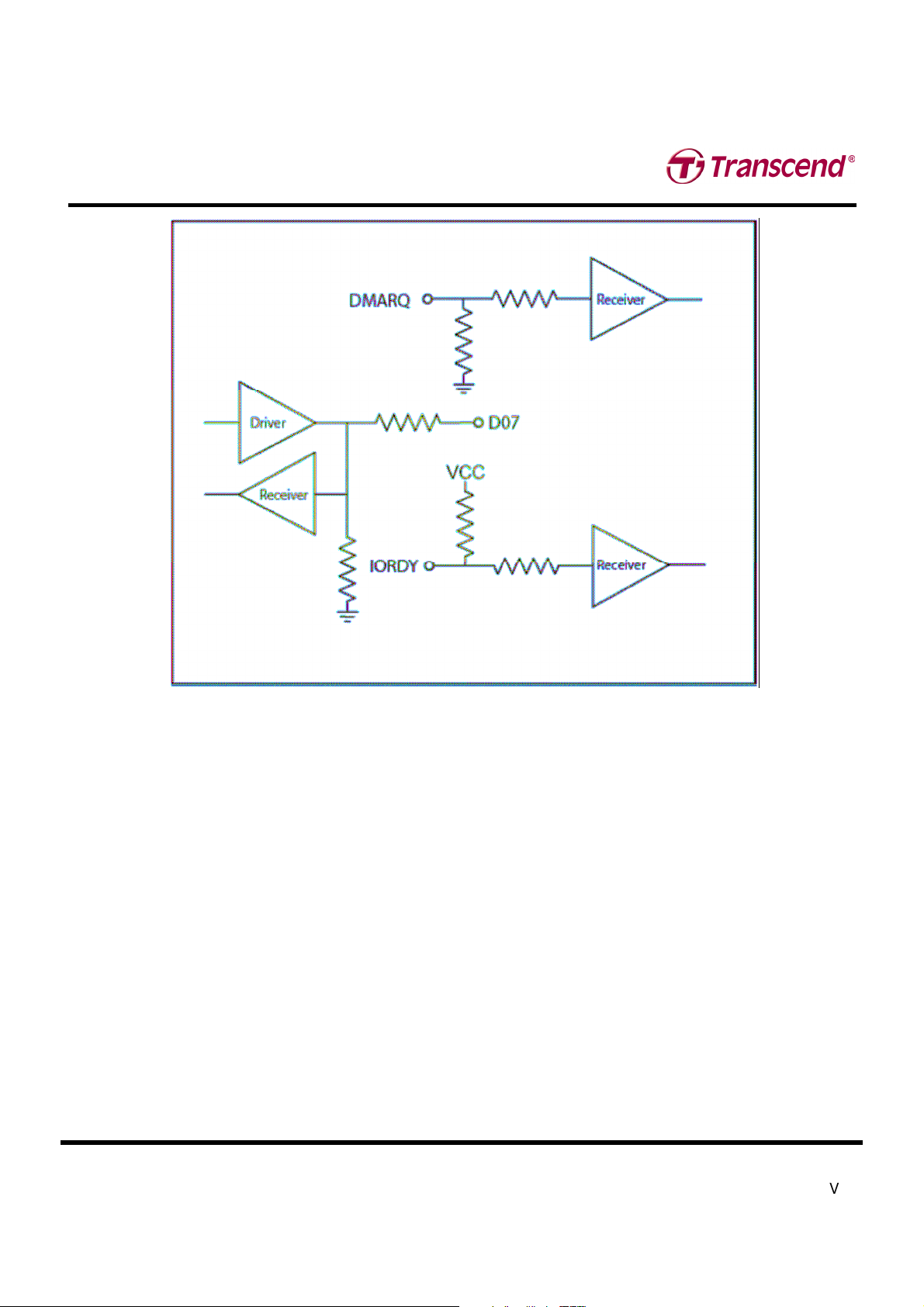
Ultra DMA Electrical Requirements
Host and Card signal capacitance limits for Ultra DMA operation
The host interface signal capacitance at the host connector shall be a maximum of 25 pF for each signal as measured at
1 MHz. The card interface signal capacitance at the card connector shall be a maximum of 20 pF for each signal as
measured at 1 MHz.
Series termination required for Ultra DMA operation
Series termination resistors are required at both the host and the card for operation in any of the Ultra DMA modes. Table
13 describes typical values for series termination at the host and the device.
Table: Typical Series Termination for Ultra DMA
Signal
T
T
T
r
r
r
a
a
a
n
n
n
s
s
s
c
c
c
e
e
e
n
n
n
d
d
d
I
I
I
n
n
n
d
d
d
u
u
u
s
s
s
t
t
t
r
r
r
i
i
i
a
a
a
l
l
l
C
C
C
F
F
F
C
C
C
a
a
a
r
r
r
d
d
d
T
T
T
S
S
S
1
1
1
2
2
2
8
8
8
M
M
M
~
~
~
1
1
1
6
6
6
G
G
G
C
C
C
F
F
F
2
2
2
0
0
0
0
0
0
I
I
I
Transcend Information Inc.
V1.2
21
Printed Circuit Board (PCB) Trace Requirements for Ultra DMA
On any PCB for a host or device supporting Ultra DMA:
The longest D[15:00] trace shall be no more than 0.5" longer than either STROBE trace as measured from the
IC pin to the connector.
The shortest D[15:00] trace shall be no more than 0.5" shorter than either STROBE trace as measured from
the IC pin to the connector.
Ultra DMA Mode Cabling Requirement
Operation in Ultra DMA mode requires a crosstalk suppressing cable. The cable shall have a grounded line
between each signal line.
For True IDE mode operation using a cable with IDE (ATA) type 40 pin connectors it is recommended that the
host sense the cable type using the method described in the ANSI INCITS 361-2002 AT Attachment - 6
standard, to prevent use of Ultra DMA with a 40 conductor cable.
Table: Ultra DMA Termination with Pull-up or Pull down Example
T
T
T
r
r
r
a
a
a
n
n
n
s
s
s
c
c
c
e
e
e
n
n
n
d
d
d
I
I
I
n
n
n
d
d
d
u
u
u
s
s
s
t
t
t
r
r
r
i
i
i
a
a
a
l
l
l
C
C
C
F
F
F
C
C
C
a
a
a
r
r
r
d
d
d
T
T
T
S
S
S
1
1
1
2
2
2
8
8
8
M
M
M
~
~
~
1
1
1
6
6
6
G
G
G
C
C
C
F
F
F
2
2
2
0
0
0
0
0
0
I
I
I
Transcend Information Inc.
V1.2
22
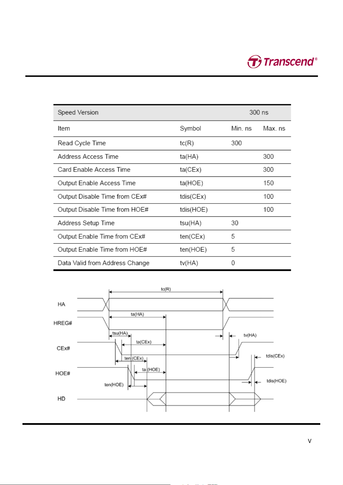
Attribute Memory Read Timing Specification

T
T
T
r
r
r
a
a
a
n
n
n
s
s
s
c
c
c
e
e
e
n
n
n
d
d
d
I
I
I
n
n
n
d
d
d
u
u
u
s
s
s
t
t
t
r
r
r
i
i
i
a
a
a
l
l
l
C
C
C
F
F
F
C
C
C
a
a
a
r
r
r
d
d
d
T
T
T
S
S
S
1
1
1
2
2
2
8
8
8
M
M
M
~
~
~
1
1
1
6
6
6
G
G
G
C
C
C
F
F
F
2
2
2
0
0
0
0
0
0
I
I
I
Transcend Information Inc.
V1.2
23
Configuration Register (Attribute Memory) Write Timing Specification

T
T
T
r
r
r
a
a
a
n
n
n
s
s
s
c
c
c
e
e
e
n
n
n
d
d
d
I
I
I
n
n
n
d
d
d
u
u
u
s
s
s
t
t
t
r
r
r
i
i
i
a
a
a
l
l
l
C
C
C
F
F
F
C
C
C
a
a
a
r
r
r
d
d
d
T
T
T
S
S
S
1
1
1
2
2
2
8
8
8
M
M
M
~
~
~
1
1
1
6
6
6
G
G
G
C
C
C
F
F
F
2
2
2
0
0
0
0
0
0
I
I
I
Transcend Information Inc.
V1.2
24
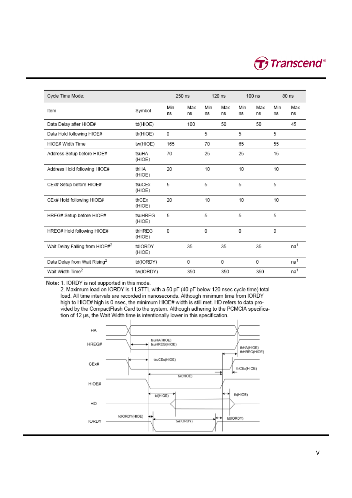
Common Memory Read Timing Specification

T
T
T
r
r
r
a
a
a
n
n
n
s
s
s
c
c
c
e
e
e
n
n
n
d
d
d
I
I
I
n
n
n
d
d
d
u
u
u
s
s
s
t
t
t
r
r
r
i
i
i
a
a
a
l
l
l
C
C
C
F
F
F
C
C
C
a
a
a
r
r
r
d
d
d
T
T
T
S
S
S
1
1
1
2
2
2
8
8
8
M
M
M
~
~
~
1
1
1
6
6
6
G
G
G
C
C
C
F
F
F
2
2
2
0
0
0
0
0
0
I
I
I
Transcend Information Inc.
V1.2
25
Common Memory Write Timing Specification
T
T
T
r
r
r
a
a
a
n
n
n
s
s
s
c
c
c
e
e
e
n
n
n
d
d
d
I
I
I
n
n
n
d
d
d
u
u
u
s
s
s
t
t
t
r
r
r
i
i
i
a
a
a
l
l
l
C
C
C
F
F
F
C
C
C
a
a
a
r
r
r
d
d
d
T
T
T
S
S
S
1
1
1
2
2
2
8
8
8
M
M
M
~
~
~
1
1
1
6
6
6
G
G
G
C
C
C
F
F
F
2
2
2
0
0
0
0
0
0
I
I
I
Transcend Information Inc.
V1.2
26
I/O Input (Read) Timing Specification

T
T
T
r
r
r
a
a
a
n
n
n
s
s
s
c
c
c
e
e
e
n
n
n
d
d
d
I
I
I
n
n
n
d
d
d
u
u
u
s
s
s
t
t
t
r
r
r
i
i
i
a
a
a
l
l
l
C
C
C
F
F
F
C
C
C
a
a
a
r
r
r
d
d
d
T
T
T
S
S
S
1
1
1
2
2
2
8
8
8
M
M
M
~
~
~
1
1
1
6
6
6
G
G
G
C
C
C
F
F
F
2
2
2
0
0
0
0
0
0
I
I
I
Transcend Information Inc.
V1.2
27
I/O Output (Write) Timing Specification
 Loading...