


Transcend TS2GDOM40V-S, TS256MDOM40V, TS32MDOM40V, TS8GDOM40V, TS64MDOM40V DATASHEET
...Transcend 40-Pin IDE Flash Module
TS128M ~ 16GDOM40V-S
Description
With an IDE interface and strong data retention ability, 40-Pin IDE Flash Modules are ideal for use in the harsh environments where Industrial PCs, Set-Top Boxes, etc. are used.
Placement
Features
•RoHS compliant products
•Storage Capacity: 128MB ~ 16GB
•Operating Voltage: 3.3V ±5% or 5V ±10%
•Operating Temperature: 0°C ~ 70°C
•Operating Humidity (Non condensation): 0% to 95%
•Storage Humidity (Non condensation): 0% to 95%
•Endurance: 2,000,000 Program/Erase cycles
•MTBF: 1,000,000 hours
•Durability of Connector: 10,000 times
•Fully compatible with devices and OS that support the IDE standard (pitch = 2.54mm)
•Built-in ECC function assures high reliability of data transfer
•Supports up to Ultra DMA Mode 4
•Supports PIO Mode 6
•Support Wear-Leveling to extend product life
Dimensions
Side |
Millimeters |
Inches |
|
|
|
A |
61.00 ± 0.40 |
2.402 ± 0.016 |
|
|
|
B |
27.10 ± 0.50 |
1.067 ± 0.020 |
|
|
|
C |
7.10 ± 0.20 |
0.280 ± 0.008 |
|
|
|
Transcend Information Inc. |
1 |
Ver 1.2
Transcend 40-Pin IDE Flash Module
TS128M ~ 16GDOM40V-S
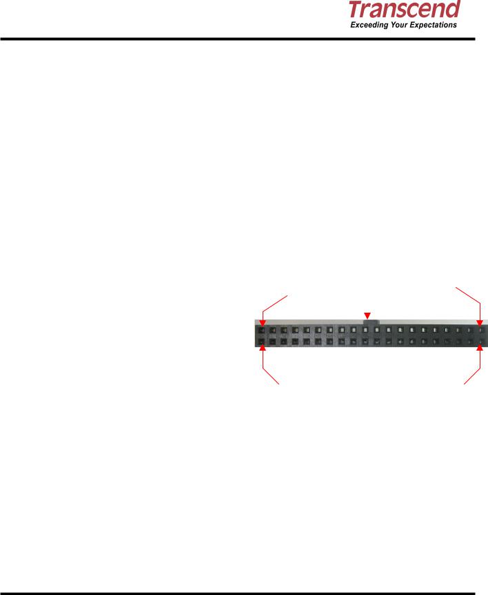
Pin Assignments
Pin |
Pin |
Pin |
Pin |
Pin |
Pin |
Pin |
Pin |
No. |
Name |
No. |
Name |
No. |
Name |
No. |
Name |
|
|
|
|
|
|
|
|
01 |
-RESET |
11 |
HD3 |
21 |
DMARQ |
31 |
IREQ |
02 |
GND |
12 |
HD12 |
22 |
GND |
32 |
IOIS16B |
03 |
HD7 |
13 |
HD2 |
23 |
IOWB |
33 |
HA1 |
04 |
HD8 |
14 |
HD13 |
24 |
GND |
34 |
PDIAGB |
05 |
HD6 |
15 |
HD1 |
25 |
IORB |
35 |
HA0 |
06 |
HD9 |
16 |
HD14 |
26 |
GND |
36 |
HA2 |
07 |
HD5 |
17 |
HD0 |
27 |
IORDY |
37 |
CE1B |
08 |
HD10 |
18 |
HD15 |
28 |
NC |
38 |
CE2B |
09 |
HD4 |
19 |
GND |
29 |
-DMACK |
39 |
DASPB |
10 |
HD11 |
20 |
VCC |
30 |
GND |
40 |
GND |
Input Power
The 40-Pin IDE Flash Module offers 2 ways to get input power, either via the small power cord or through Pin 20 of the IDE connector. If Pin 20 of the IDE connector is defined as NC (No Connect), then the 40-Pin IDE Flash Module must be directly connected to your system’s power supply. If Pin 20 of the IDE connector is defined as VCC, then the 40-Pin IDE Flash Module can get necessary power without use of the power cord.
Pin Definition |
Pin Layout |
|
|
|
|
|
|
|
|
|
|
Symbol |
Function |
|
Bulge |
|
|
HD0 ~ HD15 |
Data Bus (Bi-directional) |
Pin1 |
Pin39 |
||
|
|
|
|
||
HA0 ~ HA2 |
Address Bus (Input) |
|
|
|
|
-RESET |
Device Reset (Input) |
|
|
|
|
IORB |
Device I/O Read (Input) |
|
|
|
|
IOWB |
Device I/O Write (Input) |
|
|
|
|
IOIS16B |
Transfer Type 8/16 bit (Output) |
|
|
|
|
CE1B, CE2B |
Chip Select (Input) |
|
|
|
|
PDIAGB |
Pass Diagnostic (Bi-directional) |
Pin2 |
|
|
Pin40 |
DASPB |
Disk Active/Slave Present |
|
|
|
|
(Bi-directional) |
|
|
|
|
|
|
|
|
|
|
|
DMARQ |
DMA request |
|
|
|
|
DMACK- |
DMA acknowledge |
|
|
|
|
IREQ |
Interrupt Request (Output) |
|
|
|
|
NC |
No Connection |
|
|
|
|
GND |
Ground |
|
|
|
|
VCC |
Vcc Power Input |
|
|
|
|
Transcend Information Inc. |
2 |
Ver 1.2

Transcend 40-Pin IDE Flash Module
TS128M ~ 16GDOM40V-S
Block Diagram
With 1 pcs of Flash Memory:
With 2 pcs of Flash Memory:
Transcend Information Inc. |
3 |
Ver 1.2

Transcend 40-Pin IDE Flash Module
TS128M ~ 16GDOM40V-S
Absolute Maximum Ratings
Symbol |
Parameter |
Min |
Max |
Unit |
VDD-VSS |
DC Power Supply |
-0.6 |
+6 |
V |
|
|
|
|
|
Ta |
Operating Temperature |
0 |
+70 |
°C |
Tst |
Storage Temperature |
-40 |
+85 |
°C |
Recommended Operating Conditions
Symbol |
Parameter |
Min |
Max |
Units |
VDD |
Power supply |
3.0 |
5.5 |
V |
VIN |
Input voltage |
0 |
VDD+0.3 |
V |
Ta |
Operating Temperature |
0 |
+70 |
°C |
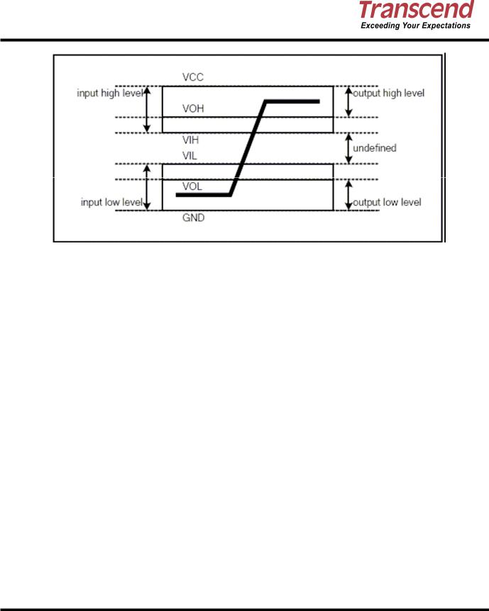
DC Characteristics
(Ta=0 oC to +70 oC, Vcc = 5.0V ±10%)
Parameter |
Symbol |
Min |
Max |
Unit |
Remark |
|
Supply Voltage |
VCC |
4.5 |
5.5 |
V |
|
|
High level output voltage |
VOH |
VCC-0.8 |
-- |
V |
|
|
Low level output voltage |
VOL |
-- |
0.8 |
V |
|
|
High level input voltage |
VIH |
4.0 |
-- |
V |
Non-schmitt trigger |
|
2.92 |
-- |
V |
Schmitt trigger1 |
|||
|
|
|||||
Low level input voltage |
VIL |
-- |
0.8 |
V |
Non-schmitt trigger |
|
-- |
1.70 |
V |
Schmitt trigger1 |
|||
|
|
|||||
(Ta=0 oC to +70 oC, Vcc = 3.3V ±5%) |
|
|
|
|||
|
|
|
|
|
|
|
Parameter |
Symbol |
Min |
Max |
Unit |
Remark |
|
Supply Voltage |
VCC |
3.135 |
3.465 |
V |
|
|
High level output voltage |
VOH |
VCC-0.8 |
-- |
V |
|
|
Low level output voltage |
VOL |
-- |
0.8 |
V |
|
|
High level input voltage |
VIH |
2.4 |
-- |
V |
Non-schmitt trigger |
|
2.05 |
-- |
V |
Schmitt trigger1 |
|||
|
|
|||||
Low level input voltage |
VIL |
-- |
0.6 |
V |
Non-schmitt trigger |
|
-- |
1.25 |
V |
Schmitt trigger1 |
|||
|
|
|||||
Transcend Information Inc. |
4 |
Ver 1.2
Transcend 40-Pin IDE Flash Module
TS128M ~ 16GDOM40V-S
Transcend Information Inc. |
5 |
Ver 1.2

Transcend 40-Pin IDE Flash Module
TS128M ~ 16GDOM40V-S
True IDE PIO Mode Read/Write Timing
|
Item |
Mode |
Mode |
Mode |
Mode |
Mode |
Mode |
Mode |
|
0 |
1 |
2 |
3 |
4 |
5 |
6 |
|
|
|
|||||||
t0 |
Cycle time (min) 1 |
600 |
383 |
240 |
180 |
120 |
100 |
80 |
t1 |
Address Valid to -IORD/-IOWR setup (min) |
70 |
50 |
30 |
30 |
25 |
15 |
10 |
t2 |
-IORD/-IOWR (min) 1 |
165 |
125 |
100 |
80 |
70 |
65 |
55 |
t2 |
-IORD/-IOWR (min) Register (8 bit) |
290 |
290 |
290 |
80 |
70 |
65 |
55 |
t2i |
-IORD/-IOWR recovery time (min) |
-- |
-- |
-- |
70 |
25 |
25 |
20 |
t3 |
-IOWR data setup (min) |
60 |
45 |
30 |
30 |
20 |
20 |
15 |
t4 |
-IOWR data hold (min) |
30 |
20 |
15 |
10 |
10 |
5 |
5 |
t5 |
-IORD data setup (min) |
50 |
35 |
20 |
20 |
20 |
15 |
10 |
t6 |
-IORD data hold (min) |
5 |
5 |
5 |
5 |
5 |
5 |
5 |
t6Z |
-IORD data tristate (max)2 |
30 |
30 |
30 |
30 |
30 |
20 |
20 |
t7 |
Address valid to IOCS16 assertion (max) 4 |
90 |
50 |
40 |
N/A |
N/A |
N/A |
N/A |
t8 |
Address valid to IOCS16 released (max) 4 |
60 |
45 |
30 |
N/A |
N/A |
N/A |
N/A |
t9 |
-IORD/-IOWR to address valid hold |
20 |
15 |
10 |
10 |
10 |
10 |
10 |
tRD |
Read Data Valid to IORDY active (min), if |
0 |
0 |
0 |
0 |
0 |
0 |
0 |
|
IORDY initially low after tA |
|||||||
|
|
|
|
|
|
|
|
|
tA |
IORDY Setup time 3 |
35 |
35 |
35 |
35 |
35 |
N/A5 |
N/A5 |
tB |
IORDY Pulse Width (max) |
1250 |
1250 |
1250 |
1250 |
1250 |
N/A5 |
N/A5 |
tC |
IORDY assertion to release (max) |
5 |
5 |
5 |
5 |
5 |
N/A5 |
N/A5 |
Notes: All timings are in nanoseconds. The maximum load on -IOCS16 is 1 LSTTL with a 50 pF (40pF below 120nsec Cycle Time) total load. All times are in nanoseconds. Minimum time from -IORDY high to -IORD high is 0 nsec, but minimum -IORD width shall still be met.
(1)t0 is the minimum total cycle time, t2 is the minimum command active time, and t2i is the minimum command recovery time or command inactive time. The actual cycle time equals the sum of the actual
command active time and the actual command inactive time. The three timing requirements of t0, t2, and t2i shall be met. The minimum total cycle time requirement is greater than the sum of t2 and t2i. This means a host implementation can lengthen either or both t2 or t2i to ensure that t0 is equal to or greater than the value reported in the device’s identify device data.
(2)This parameter specifies the time from the negation edge of -IORD to the time that the data bus is released by the device.
(3)The delay from the activation of -IORD or -IOWR until the state of IORDY is first sampled. If IORDY is inactive then the host shall wait until IORDY is active before the PIO cycle can be completed. If the device
is not driving IORDY negated at tA after the activation of -IORD or -IOWR, then t5 shall be met and tRD is not applicable. If the device is driving IORDY negated at the time tA after the activation of -IORD or -IOWR, then tRD shall be met and t5 is not applicable.
(4)t7 and t8 apply only to modes 0, 1 and 2. For other modes, this signal is not valid.
(5)IORDY is not supported in this mode.
Transcend Information Inc. |
6 |
Ver 1.2

Transcend 40-Pin IDE Flash Module
TS128M ~ 16GDOM40V-S
True IDE PIO Mode Timing Diagram
Figure 1: True IDE PIO Mode Timing Diagram
Notes:
(1)Device address consists of -CS0, -CS1, and A[02::00]
(2)Data consists of D[15::00] (16-bit) or D[07::00] (8 bit)
(3)-IOCS16 is shown for PIO modes 0, 1 and 2. For other modes, this signal is ignored.
(4)The negation of IORDY by the device is used to extend the PIO cycle. The determination of whether the cycle
is to be extended is made by the host after tA from the assertion of -IORD or -IOWR. The assertion and negation of IORDY is described in the following three cases:
(4-1) Device never negates IORDY: No wait is generated.
(4-2) Device starts to drive IORDY low before tA, but causes IORDY to be asserted before tA: No wait generated.
(4-3) Device drives IORDY low before tA: wait generated. The cycle completes after IORDY is reasserted. For cycles where a wait is generated and -IORD is asserted, the device shall place read data on D15-D00 for tRD before causing IORDY to be asserted.
Transcend Information Inc. |
7 |
Ver 1.2

Transcend 40-Pin IDE Flash Module
TS128M ~ 16GDOM40V-S
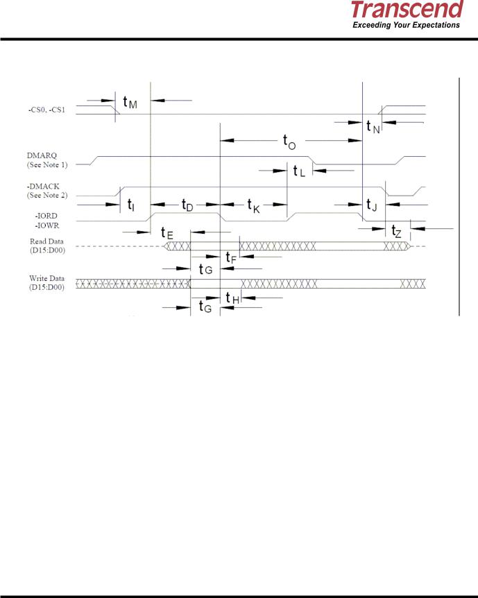
True IDE Multiword DMA Mode Read/Write Timing Specification
|
Item |
Mode 0 |
Mode 1 |
Mode 2 |
Mode 3 |
Mode 4 |
|
(ns) |
(ns) |
(ns) |
(ns) |
(ns) |
|
|
|
|||||
|
|
|
|
|
|
|
t0 |
Cycle time (min) 1 |
480 |
150 |
120 |
100 |
80 |
tD |
-IORD / -IOWR asserted width(min) 1 |
215 |
80 |
70 |
65 |
55 |
tE |
-IORD data access (max) |
150 |
60 |
50 |
50 |
45 |
tF |
-IORD data hold (min) |
5 |
5 |
5 |
5 |
5 |
tG |
-IORD/-IOWR data setup (min) |
100 |
30 |
20 |
15 |
10 |
|
|
|
|
|
|
|
tH |
-IOWR data hold (min) |
20 |
15 |
10 |
5 |
5 |
tI |
DMACK to –IORD/-IOWR setup (min) |
0 |
0 |
0 |
0 |
0 |
|
|
|
|
|
|
|
tJ |
-IORD / -IOWR to -DMACK hold (min) |
20 |
5 |
5 |
5 |
5 |
tKR |
-IORD negated width (min) 1 |
50 |
50 |
25 |
25 |
20 |
tKW |
-IOWR negated width (min) 1 |
215 |
50 |
25 |
25 |
20 |
tLR |
-IORD to DMARQ delay (max) |
120 |
40 |
35 |
35 |
35 |
|
|
|
|
|
|
|
tLW |
-IOWR to DMARQ delay (max) |
40 |
40 |
35 |
35 |
35 |
|
|
|
|
|
|
|
tM |
CS(1:0) valid to –IORD / -IOWR |
50 |
30 |
25 |
10 |
5 |
tN |
CS(1:0) hold |
15 |
10 |
10 |
10 |
10 |
tZ |
-DMACK |
20 |
25 |
25 |
25 |
25 |
|
|
|
|
|
|
|
Notes:
(1) t0 is the minimum total cycle time and tD is the minimum command active time, while tKR and tKW are the minimum command recovery time or command inactive time for input and output cycles respectively. The actual cycle time equals the sum of the actual command active time and the actual command inactive time. The three timing requirements of t0, tD, tKR, and tKW shall be met. The minimum total cycle time requirement is greater than the sum of tD and tKR or tKW.for input and output cycles respectively. This means a host implementation can lengthen either or both of tD and either of tKR, and tKW as needed to ensure that t0 is equal to or greater than the value reported in the device’s identify device data.
Transcend Information Inc. |
8 |
Ver 1.2
Transcend 40-Pin IDE Flash Module
TS128M ~ 16GDOM40V-S
True IDE Multiword DMA Mode Read/Write Timing Diagram
Figure 2: True IDE Multiword DMA Mode Read/Write Timing Diagram
Notes:
(1)If the Card cannot sustain continuous, minimum cycle time DMA transfers, it may negate DMARQ within the time specified from the start of a DMA transfer cycle to suspend the DMA transfers in progress and reassert the signal at a later time to continue the DMA operation.
(2)This signal may be negated by the host to suspend the DMA transfer in progress.
Transcend Information Inc. |
9 |
Ver 1.2

Transcend 40-Pin IDE Flash Module
TS128M ~ 16GDOM40V-S
Ultra DMA Mode Read/Write Timing Specification
Ultra DMA is an optional data transfer protocol used with the READ DMA, and WRITE DMA, commands. When this protocol is enabled, the Ultra DMA protocol shall be used instead of the Multiword DMA protocol when these commands are issued by the host. This protocol applies to the Ultra DMA data burst only. When this protocol is used there are no changes to other elements of the ATA protocol.
UDMA Signal |
Type |
TRUE IDE MODE |
|
UDMA |
|||
|
|
||
DMARQ |
Output |
DMARQ |
|
DMACK |
Input |
-DMACK |
|
STOP |
Input |
STOP1 |
|
HDMARDY(R) |
Input |
-HDMARDY1,2 |
|
HSTROBE(W) |
HSTROBE(W)1,3,4 |
||
|
|||
DDMARDY(W) |
Output |
-DDMARDY(W)1,3 |
|
DSTROBE(R) |
DSTROBE(R)1,2,4 |
||
|
|||
DATA |
Bidir |
D[15:00] |
|
ADDRESS |
Input |
A[02:00]5 |
|
CSEL |
input |
-CSEL |
|
INTRQ |
Output |
INTRQ |
|
Card Select |
Input |
-CS0 |
|
-CS1 |
|||
|
|
Notes: 1) The UDMA interpretation of this signal is valid only during an Ultra DMA data burst.
2)The UDMA interpretation of this signal is valid only during and Ultra DMA data burst during a DMA Read command.
3)The UDMA interpretation of this signal is valid only during an Ultra DMA data burst during a DMA Write command.
4)The HSTROBE and DSTROBE signals are active on both the rising and the falling edge.
5)Address lines 03 through 10 are not used in True IDE mode.
Several signal lines are redefined to provide different functions during an Ultra DMA data burst. These lines assume their UDMA definitions when:
1.an Ultra DMA mode is selected, and
2.a host issues a READ DMA, or a WRITE DMA command requiring data transfer, and
3.the device asserts (-)DMARQ, and
4.the host asserts (-)DMACK.
These signal lines revert back to the definitions used for non-Ultra DMA transfers upon the negation of -DMACK by the host at the termination of an Ultra DMA data burst.
With the Ultra DMA protocol, the STROBE signal that latches data from D[15:00] is generated by the
Transcend Information Inc. |
10 |
Ver 1.2
Transcend 40-Pin IDE Flash Module
TS128M ~ 16GDOM40V-S
same agent (either host or device) that drives the data onto the bus. Ownership of D[15:00] and this data strobe signal are given either to the device during an Ultra DMA data-in burst or to the host for an Ultra DMA data-out burst.
During an Ultra DMA data burst a sender shall always drive data onto the bus, and, after a sufficient time to allow for propagation delay, cable settling, and setup time, the sender shall generate a STROBE edge to latch the data. Both edges of STROBE are used for data transfers so that the frequency of STROBE is limited to the same frequency as the data.
Words in the IDENTIFY DEVICE data indicate support of the Ultra DMA feature and the Ultra DMA modes the device is capable of supporting. The Set transfer mode subcommand in the SET FEATURES command shall be used by a host to select the Ultra DMA mode at which the system operates. The Ultra DMA mode selected by a host shall be less than or equal to the fastest mode of which the device is capable. Only one Ultra DMA mode shall be selected at any given time. All timing requirements for a selected Ultra DMA mode shall be satisfied. Devices supporting any Ultra DMA mode shall also support all slower Ultra DMA modes.
An Ultra DMA capable device shall retain the previously selected Ultra DMA mode after executing a software reset sequence or the sequence caused by receipt of a DEVICE RESET command if a SET FEATURES disable reverting to defaults command has been issued. The device may revert to a Multiword DMA mode if a SET FEATURES enable reverting to default has been issued. An Ultra DMA capable device shall clear any previously selected Ultra DMA mode and revert to the default non-Ultra DMA modes after executing a power-on or hardware reset.
Both the host and device perform a CRC function during an Ultra DMA data burst. At the end of an Ultra DMA data burst the host sends its CRC data to the device. The device compares its CRC data to the data sent from the host. If the two values do not match, the device reports an error in the error register. If an error occurs during one or more Ultra DMA data bursts for any one command, the device shall report the first error that occurred. If the device detects that a CRC error has occurred before data transfer for the command is complete, the device may complete the transfer and report the error or abort the command and report the error.
NOTE − If a data transfer is terminated before completion, the assertion of INTRQ should be passed through to the host software driver regardless of whether all data requested by the command has been transferred.
Transcend Information Inc. |
11 |
Ver 1.2
 Loading...