


Transcend TS256MUSD, TS2GUSD-1, TS2GUSD-MS, TS512MUSD-MS, TS512MUSD DATASHEET
...TS256M~2GUSD |
|
microSD Memory Card |
||
|
|
|
|
|
Description |
|
Features |
||
Transcend microSD card series are non-volatile, |
• ROHS compliant product. |
|||
which means no external power is required to retain |
• |
Operating Voltage: 2.7 ~ 3.6V |
||
the information stored on it. Besides, it is also a |
• |
Operating Temperature: -25 ~ 85°C |
||
solid-state device that without moving parts to skip or |
• |
Durability: 10,000 insertion/removal cycles |
||
break down. Based on original NAND flash chip, |
• |
Fully compatible with SD card spec. v1.1 |
||
Transcend microSD can offer an incredible |
• |
Comply with SD Association File System Specification |
||
combination of fast data transfer, great flexibility, |
• |
Mechanical Write Protection Switch with microSD adapter |
||
excellent security and incredibly small size. |
• |
SD Host allows MultiMediaCard upward compatibility |
||
|
|
• |
Form Factor: 11mm x 15mm x 1mm |
|
Placement |
1 2 3 4 5 6 7 8 |
|
|
|
|
|
Front |
|
|
Back |
|
|
|
|
|
|
|
Pin Definition |
|
|
|
|
|
|
|
|
|
|
|
|
|
|
|
|
|
|
|
|
|
|
|
Pin No. |
|
|
SD Mode |
|
|
SPI Mode |
|
|
||
|
|
|
|
|
|
|
|
|
|
|
|
|
Name |
Type |
|
Description |
Name |
Type |
|
Description |
|
|
|
|
|
|
|
|
|
||||||
|
1 |
DAT2 |
I/O/PP |
|
Data Line [Bit2] |
RSV |
|
|
Reserved |
|
|
|
|
|
|
|
|
|
|
|
|||
|
|
|
|
|
|
|
|
|
|
|
|
|
2 |
CD/DAT3 |
I/O/PP |
|
Card Detect / Data Line [Bit3] |
CS |
I |
|
Chip Select |
|
|
|
|
|
|
|
|
|
|
|
|
|
|
|
3 |
CMD |
PP |
|
Command / Response |
DI |
I |
|
Data In |
|
|
|
|
|
|
|
|
|
|
|
|
|
|
|
4 |
VDD |
S |
|
Supply voltage |
VDD |
S |
|
Supply voltage |
|
|
|
|
|
|
|
|
|
|
|
|
|
|
|
5 |
CLK |
I |
|
Clock |
SCLK |
I |
|
Clock |
|
|
|
|
|
|
|
|
|
|
|
|
|
|
|
6 |
VSS |
S |
|
Supply voltage ground |
VSS |
S |
|
Supply voltage ground |
|
|
|
|
|
|
|
|
|
|
|
|
|
|
|
7 |
DAT0 |
I/O/PP |
|
Data Line [Bit0] |
DO |
O/PP |
|
Data out |
|
|
|
|
|
|
|
|
|
|
|
|
|
|
|
8 |
DAT1 |
I/O/PP |
|
Data Line [Bit1] |
RSV |
|
|
Reserved |
|
|
|
|
|
|
|
|
|
|
|
|
|
|
|
|
|
|
|
S: Power Supply; I:Input; O:Output; PP:Push-Pull |
|
|
|
|
||
|
|
|
|
|
|
|
|
|
|
|
|
|
|
|
|
|
|
|
|
|
|
|
|
|
Transcend Information Inc. |
1 |
|
|
|
|
|
|
|||
TS256M~2GUSD |
microSD Memory Card |
|
|
|
|
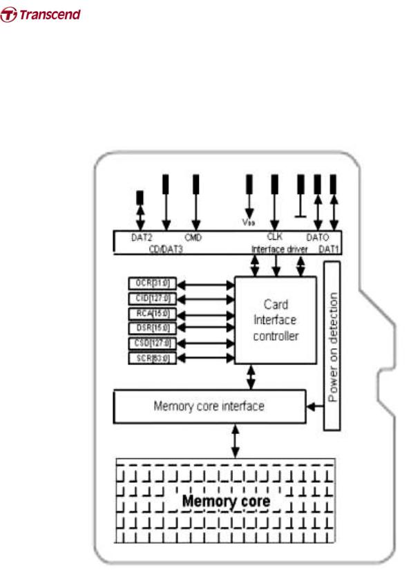
Architecture
|
|
|
|
|
|
Transcend Information Inc. |
2 |
|
|
TS256M~2GUSD |
|
|
|
|
|
microSD Memory Card |
|
|
|
|
|
|
|
|
|
|
|
Bus Operating Conditions |
|
|
|
|
|
|
|
|
• General |
|
|
|
|
|
|
|
|
Parameter |
Symbol |
|
Min. |
Max. |
Unit |
|
|
|
Peak voltage on all lines |
|
-0.3 |
VDD+0.3 |
V |
|
|
|
|
All Inputs |
|
|
|
|
|
|
|
|
Input Leakage Current |
|
|
-10 |
10 |
µA |
|
|
|
All Outputs |
|
|
|
|
|
|
|
|
Output Leakage Current |
|
|
-10 |
10 |
µA |
|
|
|
• Power Supply Voltage |
|
|
|
|
|
|
|
|
|
|
|
|
|
|
|
|
|
Parameter |
Symbol |
|
Min. |
Max. |
Unit |
|
|
|
Supply voltage |
VDD |
2.0 |
3.6 |
V |
CMD0, 15,55,ACMD41 |
||
|
|
|
|
|
|
|
commands |
|
|
Supply voltage specified in OCR register |
|
|
|
|
|
Except CMD0, 15,55, |
|
|
|
|
|
|
|
|
ACMD41 commands |
|
|
Supply voltage differentials (VSS1, VSS2) |
|
-0.3 |
0.3 |
V |
|
|
|
|
Power up time |
|
|
|
250 |
ms |
From 0v to VDD Min. |
|
Note. The current consumption of any card during the power-up procedure must not exceed 10 mA.
• Bus Signal Line Load
The total capacitance CL the CLK line of the SD Memory Card bus is the sum of the bus master capacitance CHOST, the bus capacitance CBUS itself and the capacitance CCARD of each card connected to this line:
CL = CHOST + CBUS + Ν*CCARD
Where N is the number of connected cards. Requiring the sum of the host and bus capacitances not to exceed 30 pF for up to 10 cards, and 40 pF for up to 30 cards, the following values must not be exceeded:
Parameter |
Symbol |
Min. |
Max. |
Unit |
|
|
Bus signal line capacitance |
CL |
|
100 |
pF |
fPP ≤ 20 |
MHz, 7 cards |
Single card capacitance |
CCARD |
|
10 |
pF |
|
|
Maximum signal line inductance |
|
|
16 |
nH |
fPP ≤ 20 |
MHz |
Pull-up resistance inside card (pin1) |
RDAT3 |
10 |
90 |
KΩ |
May be used for card |
|
|
|
|
|
|
detection |
|
Note that the total capacitance of CMD and DAT lines will be consist of CHOST, CBUS and one CCARD only since they are connected separately to the SD Memory Card host.
|
Parameter |
Symbol |
Min. |
Max. |
Unit |
|
|
Pull-up resistance |
RCMD, RDAT |
10 |
100 |
KΩ |
To prevent bus floating |
|
Bus signal line capacitance |
CL |
|
250 |
pF |
fPP ≤ 5 MHz, 21 cards |
|
|
|
|
|
|
|
Transcend Information Inc. |
|
3 |
|
|
|
|
TS256M~2GUSD |
microSD Memory Card |
|
|
|
|
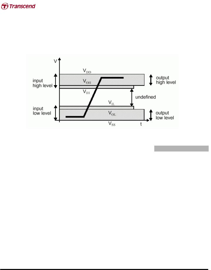
• Bus Signal Levels
As the bus can be supplied with a variable supply voltage, all signal levels are related to the supply voltage.
To meet the requirements of the JEDEC specification JESD8-1A, the card input and output voltages shall be within the following specified ranges for any VDD of the allowed voltage range:
Parameter |
Symbol |
Min. |
Max. |
Unit |
Remark |
Output HIGH voltage |
VOH |
0.75* VDD |
|
V |
IOH = -100 μA @VDD min |
Output LOW voltage |
VOL |
|
0.125* VDD |
V |
IOL = 100 μA @VDD min |
Input HIGH voltage |
VIH |
0.625* VDD |
VDD + 0.3 |
V |
|
Input LOW voltage |
VIL |
VSS – 0.3 |
0.25* VDD |
V |
|
Transcend Information Inc. |
4 |
TS256M~2GUSD |
microSD Memory Card |
|
|
|
|
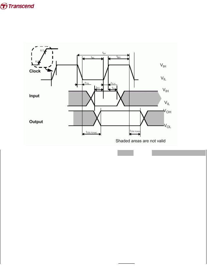
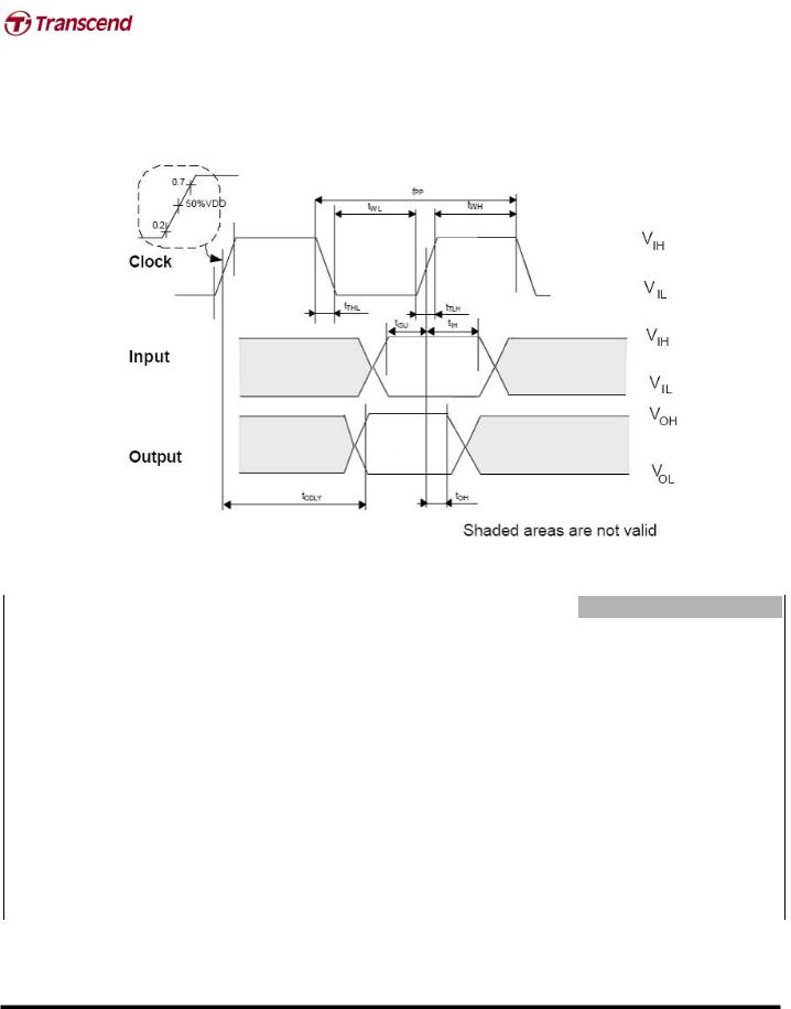
• Bus Timing (Default) |
|
|
Parameter |
Symbol |
Min |
Max. |
Unit |
Remark |
Clock CLK (All values are referred to min (VIH) and max (VIL)
|
Clock frequency Data Transfer Mode |
fPP |
0 |
25 |
MHz |
CL ≤ 100 pF, (7 cards) |
|
||
|
Clock frequency Identification Mode |
fOD |
0 |
400 |
KHz |
CL ≤ 250 pF, (21 cards) |
|
||
|
(The low freq. is required for MultiMediaCard |
|
|
|
|
|
|
|
|
|
compatibility.) |
|
|
|
|
|
|
|
|
|
Clock low time |
tWL |
10 |
|
|
ns |
CL ≤ 100 pF, (7 cards) |
|
|
|
|
|
50 |
|
|
ns |
CL ≤ 250 pF, (21 cards) |
|
|
|
Clock high time |
tWH |
10 |
|
|
ns |
CL ≤ 100 pF, (7 cards) |
|
|
|
|
|
50 |
|
|
ns |
CL ≤ 250 pF, (21 cards) |
|
|
|
Clock rise time |
tTLH |
|
|
10 |
ns |
CL ≤ 100 pF, (7 cards) |
|
|
|
|
|
|
|
50 |
ns |
CL ≤ 250 pF, (21 cards) |
|
|
|
Clock fall time |
tTHL |
|
|
10 |
ns |
CL ≤ 100 pF, (7 cards) |
|
|
|
|
|
|
|
50 |
ns |
CL ≤ 250 pF, (21 cards) |
|
|
|
Inputs CMD, DAT (referenced to CLK) |
|
|
|
|
|
|
|
|
|
Input set-up time |
tISU |
5 |
|
|
ns |
CL ≤ 25 pF, (1 cards) |
|
|
|
Input hold time |
tIH |
5 |
|
|
ns |
CL ≤ 25 pF, (1 cards) |
|
|
|
Outputs CMD, DAT (referenced to CLK) |
|
|
|
|
|
|
|
|
|
Output Delay time |
tODLY |
|
0 |
|
14 |
ns |
CL ≤ 25 pF, (1 cards) |
|
|
|
|
|
|
|
|
|
|
|
Transcend Information Inc. |
|
5 |
|
|
|
|
|
|
|
TS256M~2GUSD |
microSD Memory Card |
|
|
|
|
• Bus Timing (High-speed Mode) |
|
|
Parameter |
Symbol |
Min |
Max. |
Unit |
Remark |
Clock CLK (All values are referred to min (VIH) and max (VIL)
Clock frequency Data Transfer Mode |
fPP |
0 |
50 |
MHz |
CCARD ≤ 10 pF, (1 card) |
Clock low time |
tWL |
7 |
|
ns |
CCARD ≤ 10 pF, (1 card) |
Clock high time |
tWH |
7 |
|
ns |
CCARD ≤ 10 pF, (1 card) |
Clock rise time |
tTLH |
|
3 |
ns |
CCARD ≤ 10 pF, (1 card) |
Clock fall time |
tTHL |
|
3 |
ns |
CCARD ≤ 10 pF, (1 card) |
Inputs CMD, DAT (referenced to CLK) |
|
|
|
|
|
Input set-up time |
tISU |
6 |
|
ns |
CCARD ≤ 10 pF, (1 card) |
Input hold time |
tIH |
2 |
|
ns |
CCARD ≤ 10 pF, (1 card) |
Outputs CMD, DAT (referenced to CLK) |
|
|
|
|
|
Output Delay time during Data Transfer Mode |
tODLY |
|
14 |
ns |
CL ≤ 40 pF, (1 card) |
Output Hold time |
tOH |
2.5 |
|
ns |
CL ≤ 40 pF, (1 card) |
Total System capacitance for each line1 |
CL |
|
40 |
pF |
(1 card) |
1) In order to satisfy severe timing, host shall drive only one card.
Transcend Information Inc. |
6 |

|
TS256M~2GUSD |
microSD Memory Card |
||
|
|
|
|
|
|
Reliability and Durability |
|
|
|
|
|
|
|
|
|
Temperature |
Operation: -25°C / 85°C (Target spec) |
|
|
|
|
Storage: -40°C (168h) / 85°C (500h) |
|
|
|
|
Junction temperature: max. 95°C |
|
|
|
Moisture and corrosion |
Operation: 25°C / 95% rel. humidity |
|
|
|
|
Storage: 40°C / 93% rel. hum./500h |
|
|
|
|
Salt Water Spray: 3% NaCl/35C; 24h acc. MIL STD Method 1009 |
||
|
Durability |
10000 mating cycles |
|
|
|
Bending |
10N |
|
|
|
Torque |
0.10N*m , +/- 2.5deg max |
|
|
|
Drop test |
1.5m free fall |
|
|
|
UV light exposure |
UV: 254nm, 15Ws/cm² according to ISO 7816-1 |
|
|
|
Visual inspection |
No warppage; no mold skin; complete form; no cavities surface smoothness <= -0.1 |
||
|
Shape and form |
mm/cm² within contour; no cracks; no pollution (fat, oil dust, etc.) |
||
Above technical information is based on standard data and tested to be reliable. However, Transcend makes no warranty, either expressed or implied, as to its accuracy and assumes no liability in connection with the use of this product. Transcend reserves the right to make changes in specifications at any time without prior notice.
Transcend Information Inc. |
7 |

TS256M~2GUSD |
microSD Memory Card |
|
|
|
|
Register Information
Within the card interface six registers are defined: OCR, CID, CSD, RCA, DSR and SCR. These can be accessed only by corresponding commands (see Chapter 4.7). The OCR, CID, CSD and SCR registers carry the card/content specific information, while the RCA and DSR registers are configuration registers storing actual configuration parameters.
1. OCR register
The 32-bit operation conditions register stores the VDD voltage profile of the card. In addition, this register includes a status information bit. This status bit is set if the card power up procedure has been finished. The OCR register shall be implemented by the cards which do not support the full operating voltage range of the SD Memory Card bus, or if the card power up extends the definition in the timing diagram.
A voltage range is not supported if the corresponding bit value is set to LOW. As long as the card is busy, the corresponding bit (31) is set to LOW.
Transcend Information Inc. |
8 |
 Loading...