


TS128MCF80
Transcend TS128MCF80, TS256MCF80-P, TS64MCF80-P, TS1GCF80, TS512MCF80 QUICK INSTRUCTION GUIDE
...
T
T
T
S
S
S
3
3
3
2
2
2
M
M
M
~
~
~
1
1
1
G
G
G
C
C
C
F
F
F
8
8
8
0
0
0
80X CompactFlash Card
Transcend Information Inc.
V1.7
1
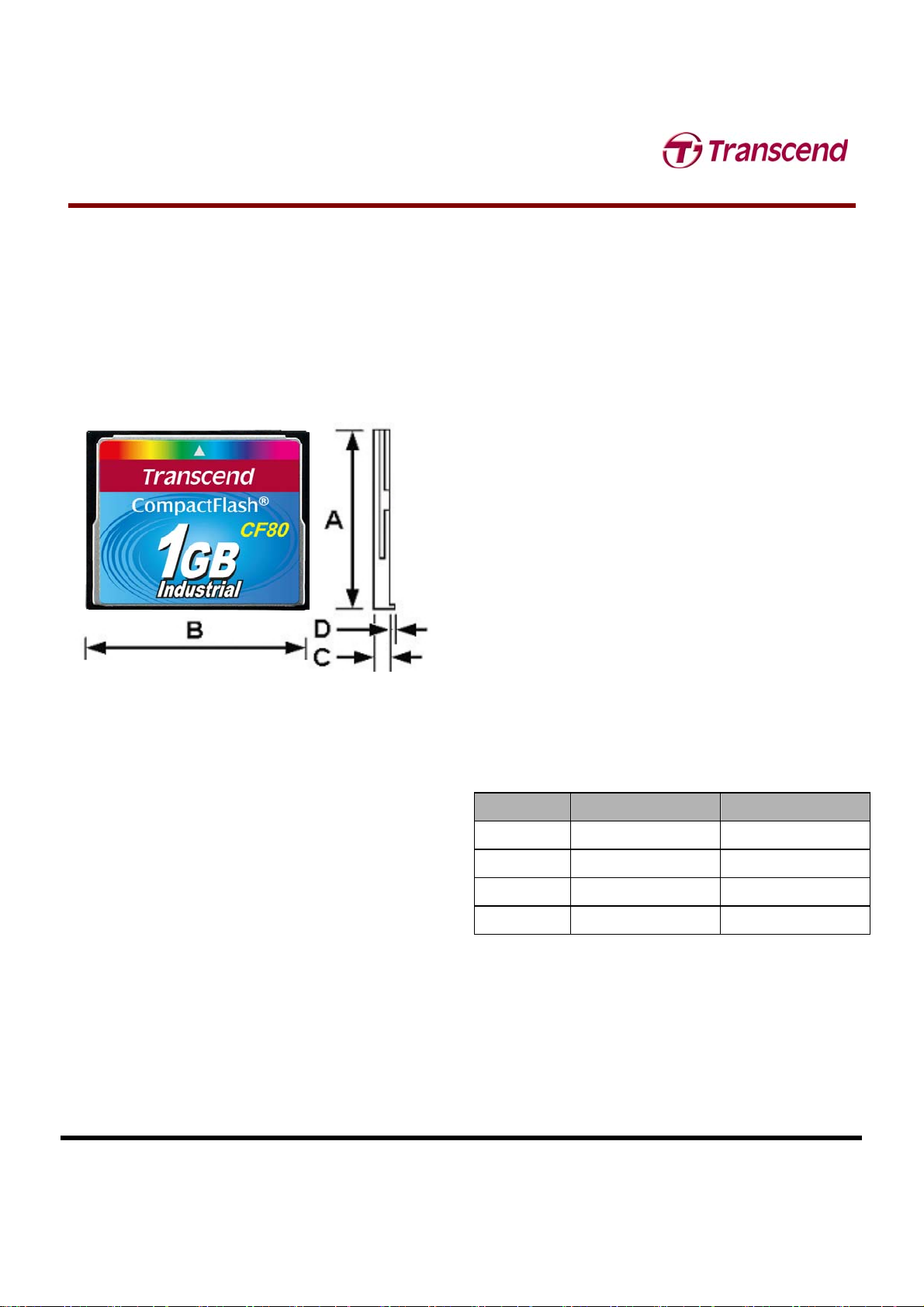
1. Description
The Transcend CF 80X is a High Speed Compact
Flash Card with high quality Flash Memory assembled
on a printed circuit board.
Placement
1.1 Feature
• RoHS compliant products
• Compliant with CompactFlash® specification V3.0
• Single Power Supply: 5V ± 10% / 3.3V ± 5%
• Compliant to CompactFlash, PCMCIA, and ATA
standards
• Support PIO mode 0 to PIO mode 6
• Support Multi-Word DMA mode 0 to Multi-Word DMA
mode 4 (Series of –P only supports PIO mode 0 to
mode 4, please see Ordering Information)
• True IDE Mode: Fixed Disk (Standard)
• PC Card Mode: Removable Disk (Standard)
• Operating Temperature: -25
o
C to 85
o
C
• Storage Temperature: -40
o
C to 85
o
C
• Operating Humidity (Non condensation): 0% to 95%
• Storage Humidity (Non condensation): 0% to 95%
• Hardware RS-code ECC
• Support Wear-Leveling to extend product life
• Durability of Connector: 10,000 times
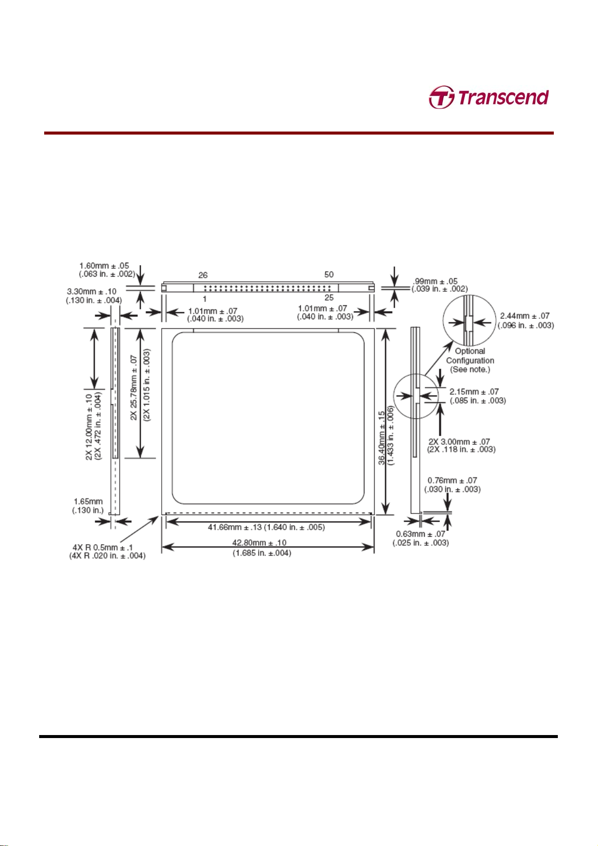
1.2 Dimensions
Side Millimeters Inches
A 36.40 ± 0.150 1.43 ± 0.005
B 42.80 ± 0.100 1.69 ± 0.004
C 3.30 ± 0.100 0.13 ± 0.004
D 0.63 ± 0.070 0.02 ± 0.003

T
T
T
S
S
S
3
3
3
2
2
2
M
M
M
~
~
~
1
1
1
G
G
G
C
C
C
F
F
F
8
8
8
0
0
0
80X CompactFlash Card
Transcend Information Inc.
V1.7
2
1.3 Ordering Information
1.4 CHS and Capacity
Product Name Cylinder Head Sector Capacity
TS32MCF80 62 16 63 29.9MB
TS64MCF80 125 16 63 60.8MB
TS128MCF80 246 16 63 120MB
TS256MCF80 500 16 63 245MB
TS512MCF80 989 16 63 486MB
TS1GCF80 1978 16 63 972MB
Part Number Mode Description Transfer mode
True IDE mode DMA Fixed Disk Multiword DMA mode 0~4, PIO mode 0~6
TS32M~1GCF80
PCMCIA mode Non-DMA Removable Disk N/A
True IDE mode Non-DMA Fixed Disk PIO mode 0~4
CF80
TS32M~1GCF80-P
PCMCIA mode Non-DMA Removable Disk N/A
T
T
T
S
S
S
3
3
3
2
2
2
M
M
M
~
~
~
1
1
1
G
G
G
C
C
C
F
F
F
8
8
8
0
0
0
80X CompactFlash Card
Transcend Information Inc.
V1.7
3
2.Product Specification
2.1 Compactflash Card Specification
Transcend
T
T
T
S
S
S
3
3
3
2
2
2
M
M
M
~
~
~
1
1
1
G
G
G
C
C
C
F
F
F
8
8
8
0
0
0
80X CompactFlash Card
Transcend Information Inc.
V1.7
4
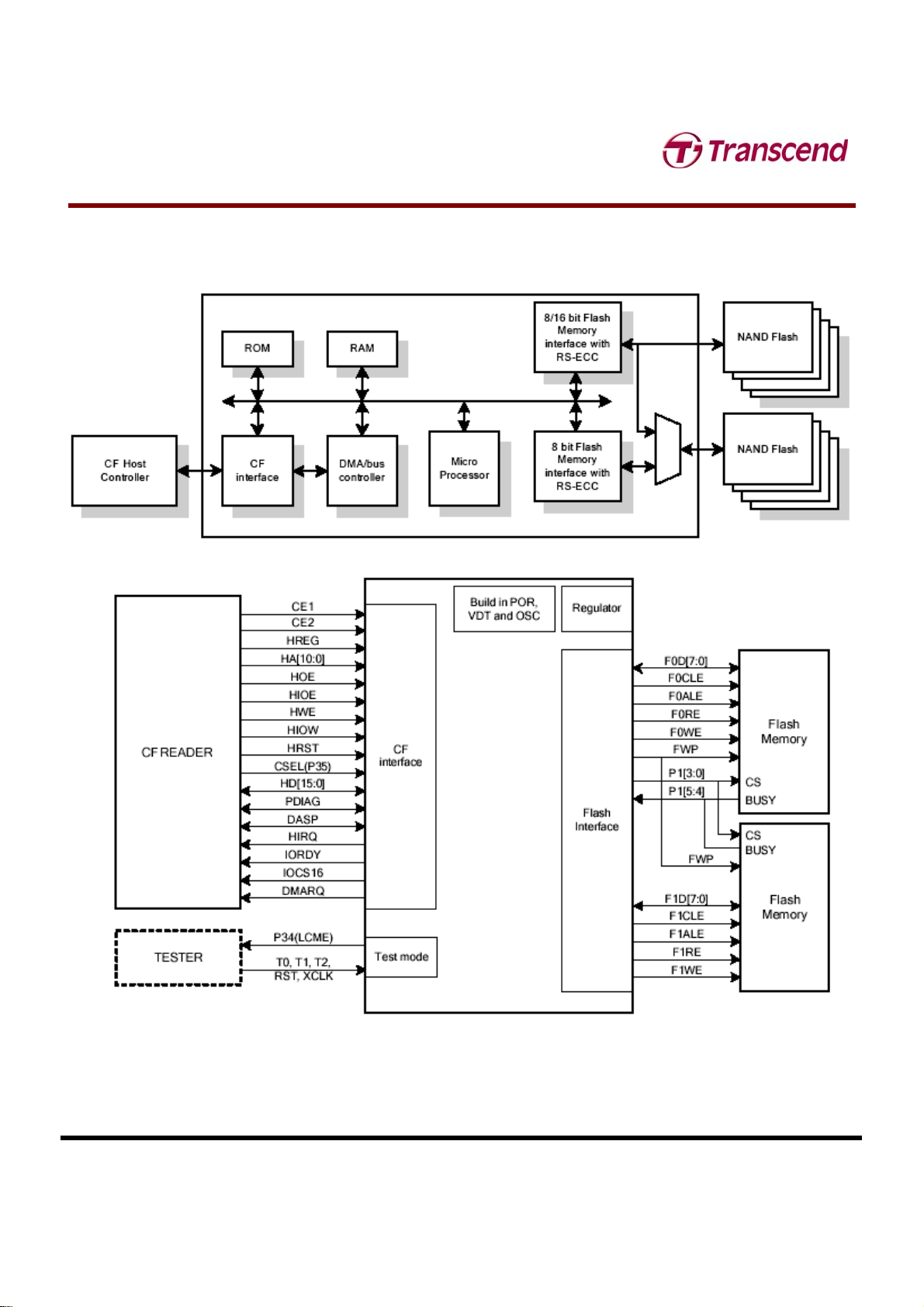
2.2 Block Diagram
T
T
T
S
S
S
3
3
3
2
2
2
M
M
M
~
~
~
1
1
1
G
G
G
C
C
C
F
F
F
8
8
8
0
0
0
80X CompactFlash Card
Transcend Information Inc.
V1.7
5
3. Electrical Interface
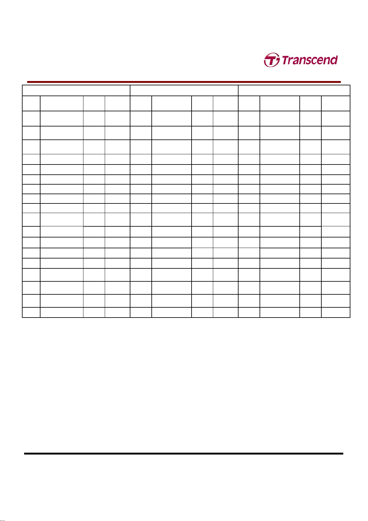
3.1 Pin Assignment and Pin Type
PC Card Memory Mode PC Card I/O Mode
True IDE Mode
4
Pin
Num
Signal
Name
Pin
Type
In, Out Type Pin Num
Signal
Name
Pin
Type
In, Out
Type
Pin
Num
Signal
Name
Pin
Type
In, Out
Type
1 GND
Ground 1 GND
Ground 1 GND
Ground
2 D03 I/O I1Z, OZ3 2 D03 I/O I1Z, OZ3 2 D03 I/O I1Z, OZ3
3 D04 I/O I1Z, OZ3 3 D04 I/O I1Z, OZ3 3 D04 I/O I1Z, OZ3
4 D05 I/O I1Z, OZ3 4 D05 I/O I1Z, OZ3 4 D05 I/O I1Z, OZ3
5 D06 I/O I1Z, OZ3 5 D06 I/O I1Z, OZ3 5 D06 I/O I1Z, OZ3
6 D07 I/O I1Z, OZ3 6 D07 I/O I1Z, OZ3 6 D07 I/O I1Z, OZ3
7 -CE1 I I3U 7 -CE1 I I3U 7 -CS0 I I3Z
8 A10 I I1Z 8 A10 I I1Z 8 A10
2
I I1Z
9 -OE I I3U 9 -OE I I3U 9 -ATA SEL I I3U
10 A09 I I1Z 10 A09 I I1Z 10 A09
2
I I1Z
11 A08 I I1Z 11 A08 I I1Z 11 A08
2
I I1Z
12 A07 I I1Z 12 A07 I I1Z 12 A07
2
I I1Z
13 VCC
Power 13 VCC
Power 13 VCC
Power
14 A06 I I1Z 14 A06 I I1Z 14 A06
2
I I1Z
15 A05 I I1Z 15 A05 I I1Z 15 A05
2
I I1Z
16 A04 I I1Z 16 A04 I I1Z 16 A04
2
I I1Z
17 A03 I I1Z 17 A03 I I1Z 17 A03
2
I I1Z
18 A02 I I1Z 18 A02 I I1Z 18 A02 I I1Z
19 A01 I I1Z 19 A01 I I1Z 19 A01 I I1Z
20 A00 I I1Z 20 A00 I I1Z 20 A00 I I1Z
21 D00 I/O I1Z, OZ3 21 D00 I/O I1Z, OZ3 21 D00 I/O I1Z, OZ3
22 D01 I/O I1Z, OZ3 22 D01 I/O I1Z, OZ3 22 D01 I/O I1Z, OZ3
23 D02 I/O I1Z, OZ3 23 D02 I/O I1Z, OZ3 23 D02 I/O I1Z, OZ3
24 WP O OT3 24 -IOIS16 O OT3 24 -IOCS16 O ON3
25 -CD2 O Ground 25 -CD2 O Ground 25 -CD2 O Ground
26 -CD1 O Ground 26 -CD1 O Ground 26 -CD1 O Ground
27 D11
1
I/O I1Z, OZ3 27 D11
1
I/O I1Z, OZ3 27 D11
1
I/O I1Z, OZ3
28 D121 I/O I1Z, OZ3 28 D12
1
I/O I1Z, OZ3 28 D12
1
I/O I1Z, OZ3
29 D13
1
I/O I1Z, OZ3 29 D13
1
I/O I1Z, OZ3 29 D13
1
I/O I1Z, OZ3
30 D14
1
I/O I1Z, OZ3 30 D14
1
I/O I1Z, OZ3 30 D14
1
I/O I1Z, OZ3
31 D15
1
I/O I1Z, OZ3 31 D15
1
I/O I1Z, OZ3 31 D15
1
I/O I1Z, OZ3
32 -CE2
1
I I3U 32 -CE2
1
I I3U 32 -CS1
1
I I3Z
T
T
T
S
S
S
3
3
3
2
2
2
M
M
M
~
~
~
1
1
1
G
G
G
C
C
C
F
F
F
8
8
8
0
0
0
80X CompactFlash Card
Transcend Information Inc.
V1.7
6
PC Card Memory Mode PC Card I/O Mode
True IDE Mode
4
Pin
Num
Signal Name
Pin
Type
In, Out
Type
Pin
Num
Signal Name
Pin
Type
In, Out
Type
Pin
Num
Signal Name
Pin
Type
In, Out
Type
33 -VS1 O Ground 33 -VS1 O Ground 33 -VS1 O Ground
34 -IORD I I3U 34 -IORD I I3U 34 -IORD I I3Z
35 -IOWR I I3U 35 -IOWR I I3U 35 -IOWR I I3Z
36 -WE I I3U 36 -WE I I3U 36 -WE
3
I I3U
37 READY O OT1 37 -IREQ O OT1 37 INTRQ O OZ1
38 VCC Power 38 VCC Power 38 VCC Power
39 -CSEL
5
I I2Z 39 -CSEL
5
I I2Z 39 -CSEL I I2U
40 -VS2 O OPEN 40 -VS2 O OPEN 40 -VS2 O OPEN
41 RESET I I2Z 41 RESET I I2Z 41 -RESET I I2Z
42 -WAIT O OT1 42 -WAIT O OT1 42 IORDY O ON1
43 -INPACK O OT1 43 -INPACK O OT1 43 DMARQ O OZ1
44 -REG I I3U 44 -REG I I3U 44 -DMACK
6
I I3U
45 BVD2 O OT1 45 -SPKR O OT1 45 -DASP I/O I1U, ON1
46 BVD1 O OT1 46 -STSCHG O OT1 46 -PDIAG I/O I1U, ON1
47 D08
1
I/O
I1Z,
OZ3
47 D08
1
I/O
I1Z,
OZ3
47 D08
1
I/O I1Z, OZ3
48 D09
1
I/O
I1Z,
OZ3
48 D09
1
I/O
I1Z,
OZ3
48 D09
1
I/O I1Z, OZ3
49 D10
1
I/O
I1Z,
OZ3
49 D10
1
I/O
I1Z,
OZ3
49 D10
1
I/O I1Z, OZ3
50 GND Ground 50 GND Ground 50 GND Ground
Note:
1) These signals are required only for 16 bit accesses and not required when installed in 8 bit systems. Devices
should allow for 3-state signals not to consume current.
2) The signal should be grounded by the host.
3) The signal should be tied to VCC by the host.
4) The mode is required for CompactFlash Storage Cards.
5) The -CSEL signal is ignored by the card in PC Card modes. However, because it is not pulled upon the card in these
modes, it should not be left floating by the host in PC Card modes. In these modes, the pin should be connected by the
host to PC Card A25 or grounded by the host.
6) If DMA operations are not used, the signal should be held high or tied to VCC by the host. For proper operation in older
hosts: while DMA operations are not active, the card shall ignore this signal,including a floating condition

T
T
T
S
S
S
3
3
3
2
2
2
M
M
M
~
~
~
1
1
1
G
G
G
C
C
C
F
F
F
8
8
8
0
0
0
80X CompactFlash Card
Transcend Information Inc.
V1.7
7
3.2 Signal Description
Signal Name Dir. Pin Description
A10 – A00
(PC Card Memory Mode)
A10 – A00
(PC Card I/O Mode)
A02 - A00
(True IDE Mode)
I
I
8,10,11,12,
14,15,16,17,
18,19,20
18,19,20
These address lines along with the -REG signal are used to select the following:
The I/O port address registers within the CompactFlash Storage Card , the
memory mapped port address registers within the CompactFlash Storage Card,
a byte in the card's information structure and its configuration control and status
registers.
This signal is the same as the PC Card Memory Mode signal.
In True IDE Mode, only A[02:00] are used to select the one of eight registers
in the Task File, the remaining address lines should be grounded by the host.
BVD1
(PC Card Memory Mode)
-STSCHG
(PC Card I/O Mode)
Status Changed
-PDIAG
(True IDE Mode)
I/O 46 This signal is asserted high, as BVD1 is not supported.
This signal is asserted low to alert the host to changes in the READY and Write
Protect states, while the I/O interface is configured. Its use is controlled by the
Card Config and Status Register.
In the True IDE Mode, this input / output is the Pass Diagnostic signal in the
Master / Slave handshake protocol.
BVD2
(PC Card Memory Mode)
-SPKR
(PC Card I/O Mode)
-DASP
(True IDE Mode)
I/O 45 This signal is asserted high, as BVD2 is not supported.
This line is the Binary Audio output from the card. If the Card does not support
the Binary Audio function, this line should be held negated.
In the True IDE Mode, this input/output is the Disk Active/Slave Present signal in
the Master/Slave handshake protocol.
-CD1, -CD2
(PC Card Memory Mode)
-CD1, -CD2
(PC Card I/O Mode)
-CD1, -CD2
(True IDE Mode)
O 26,25 These Card Detect pins are connected to ground on the CompactFlash Storage
Card. They are used by the host to determine that the CompactFlash Storage
Card is fully inserted into its socket.
This signal is the same for all modes.
This signal is the same for all modes.

T
T
T
S
S
S
3
3
3
2
2
2
M
M
M
~
~
~
1
1
1
G
G
G
C
C
C
F
F
F
8
8
8
0
0
0
80X CompactFlash Card
Transcend Information Inc.
V1.7
8
Signal Name Dir. Pin Description
-CE1, -CE2
(PC Card Memory Mode)
Card Enable
-CE1, -CE2
(PC Card I/O Mode)
Card Enable
-CS0, -CS1
(True IDE Mode)
I 7,32
These input signals are used both to select the card and to indicate to the card
whether a byte or a word operation is being performed. -CE2 always accesses
the odd byte of the word.-CE1 accesses the even byte or the Odd byte of the
word depending on A0 and -CE2. A multiplexing scheme based on A0,-CE1,
-CE2 allows 8 bit hosts to access all data on D0-D7. See Table 27, Table 29,
Table 31, Table 35, Table 36 and Table 37.
This signal is the same as the PC Card Memory Mode signal.
In the True IDE Mode, -CS0 is the address range select for the task file
registers while -CS1 is used to select the Alternate Status Register and the
Device Control Register.
While –DMACK is asserted, -CS0 and –CS1 shall be held negated and the
width of the transfers shall be 16 bits.
-CSEL
(PC Card Memory Mode)
-CSEL
(PC Card I/O Mode)
-CSEL
(True IDE Mode)
I 39 This signal is not used for this mode, but should be connected by the host to PC
Card A25 or grounded by the host.
This signal is not used for this mode, but should be connected by the host to PC
Card A25 or grounded by the host.
This internally pulled up signal is used to configure this device as a Master or a
Slave when configured in the True IDE Mode.
When this pin is grounded, this device is configured as a Master.
When the pin is open, this device is configured as a Slave.
D15 - D00
(PC Card Memory Mode)
D15 - D00
(PC Card I/O Mode)
D15 - D00
(True IDE Mode)
I/O
31,30,29,28,
27,49,48,47,
6,5,4,3,2,
23, 22, 21
These lines carry the Data, Commands and Status information between the host
and the controller. D00 is the LSB of the Even Byte of the Word. D08 is the LSB
of the Odd Byte of the Word.
This signal is the same as the PC Card Memory Mode signal.
In True IDE Mode, all Task File operations occur in byte mode on the low order
bus D[7:0] while all data transfers are 16 bit using D[15:0].
GND
(PC Card Memory Mode)
GND
(PC Card I/O Mode)
GND
(True IDE Mode)
-- 1,50 Ground.
This signal is the same for all modes.
This signal is the same for all modes.

T
T
T
S
S
S
3
3
3
2
2
2
M
M
M
~
~
~
1
1
1
G
G
G
C
C
C
F
F
F
8
8
8
0
0
0
80X CompactFlash Card
Transcend Information Inc.
V1.7
9
Signal Name Dir. Pin Description
-INPACK
(PC Card Memory Mode)
-INPACK
(PC Card I/O Mode)
Input Acknowledge
DMARQ
(True IDE Mode)
O 43 This signal is not used in this mode.
The Input Acknowledge signal is asserted by the CompactFlash Storage Card
when the card is selected and responding to an I/O read cycle at the address that
is on the address bus. This signal is used by the host to control the enable of any
input data buffers between the CompactFlash Storage Card and the CPU.
This signal is a DMA Request that is used for DMA data transfers between host
and device. It shall be asserted by the device when it is ready to transfer data to
or from the host. For Multiword DMA transfers, the direction of data transfer is
controlled by -IORD and -IOWR. This signal is used in a handshake manner with
-DMACK, i.e., the device shall wait until the host asserts -DMACK before
negating DMARQ, and reasserting DMARQ if there is more data to transfer.
DMARQ shall not be driven when the device is not selected.
While a DMA operation is in progress, -CS0 and –CS1 shall be held negated and
the width of the transfers shall be 16 bits.
If there is no hardware support for DMA mode in the host, this output signal is not
used and should not be connected at the host. In this case, the BIOS must report
that DMA mode is not supported by the host so that device drivers will not
attempt DMA mode.
A host that does not support DMA mode and implements both PCMCIA and
True-IDE modes of operation need not alter the PCMCIA mode connections
while in True-IDE mode as long as this does not prevent proper operation in any
mode.
-IORD
(PC Card Memory Mode)
-IORD
(PC Card I/O Mode)
-IORD
(True IDE Mode )
I 34 This signal is not used in this mode.
This is an I/O Read strobe generated by the host. This signal gates I/O data onto
the bus from the CompactFlash Storage Card when the card is configured to use
the I/O interface.
In True IDE Mode, this signal has the same function as in PC Card I/O Mode.
-IOWR
(PC Card Memory Mode)
-IOWR
(PC Card I/O Mode)
-IOWR
(True IDE Mode)
I 35
This signal is not used in this mode.
The I/O Write strobe pulse is used to clock I/O data on the Card Data bus into the
CompactFlash Storage Card controller registers when the CompactFlash
Storage Card is configured to use the I/O interface.
The clocking shall occur on the negative to positive edge of the signal (trailing
edge).
In True IDE Mode, this signal has the same function as in PC Card I/O Mode.

T
T
T
S
S
S
3
3
3
2
2
2
M
M
M
~
~
~
1
1
1
G
G
G
C
C
C
F
F
F
8
8
8
0
0
0
80X CompactFlash Card
Transcend Information Inc.
V1.7
10
Signal Name Dir. Pin Description
-OE
(PC Card Memory Mode)
-OE
(PC Card I/O Mode)
-ATA SEL
(True IDE Mode)
I 9
This is an Output Enable strobe generated by the host interface. It is used to read
data from the CompactFlash Storage Card in Memory Mode and to read the CIS
and configuration registers.
In PC Card I/O Mode, this signal is used to read the CIS and configuration
registers.
To enable True IDE Mode this input should be grounded by the host.
READY
(PC Card Memory Mode)
-IREQ
(PC Card I/O Mode)
INTRQ
(True IDE Mode)
O 37
In Memory Mode, this signal is set high when the CompactFlash Storage Card is
ready to accept a new data transfer operation and is held low when the card is
busy.
At power up and at Reset, the READY signal is held low (busy) until the
CompactFlash Storage Card has completed its power up or reset function. No
access of any type should be made to the CompactFlash Storage Card during
this time.
Note, however, that when a card is powered up and used with RESET
continuously disconnected or asserted, the Reset function of the RESET pin is
disabled. Consequently, the continuous assertion of RESET from the application
of power shall not cause the READY signal to remain continuously in the busy
state.
I/O Operation – After the CompactFlash Storage Card Card has been configured
for I/O operation, this signal is used as -Interrupt Request. This line is strobed
low to generate a pulse mode interrupt or held low for a level mode interrupt.
In True IDE Mode signal is the active high Interrupt Request to the host.
-REG
(PC Card Memory Mode)
Attribute Memory Select
-REG
(PC Card I/O Mode)
I 44
This signal is used during Memory Cycles to distinguish between Common
Memory and Register (Attribute) Memory accesses. High for Common Memory,
Low for Attribute Memory.
The signal shall also be active (low) during I/O Cycles when the I/O address is on
the Bus.
-DMACK
(True IDE Mode)
This is a DMA Acknowledge signal that is asserted by the host in response to
DMARQ to initiate DMA transfers.
While DMA operations are not active, the card shall ignore the -DMACK signal,
including a floating condition.
If DMA operation is not supported by a True IDE Mode only host, this signal
should be driven high or connected to VCC by the host.
A host that does not support DMA mode and implements both PCMCIA and
True-IDE modes of operation need not alter the PCMCIA mode connections
while in True-IDE mode as long as this does not prevent proper operation all
modes.

T
T
T
S
S
S
3
3
3
2
2
2
M
M
M
~
~
~
1
1
1
G
G
G
C
C
C
F
F
F
8
8
8
0
0
0
80X CompactFlash Card
Transcend Information Inc.
V1.7
11
Signal Name Dir. Pin Description
RESET
(PC Card Memory Mode)
RESET
(PC Card I/O Mode)
-RESET
(True IDE Mode)
I 41 The CompactFlash Storage Card is Reset when the RESET pin is high with the
following important exception:
The host may leave the RESET pin open or keep it continually high from the
application of power without causing a continuous Reset of the card. Under
either of these conditions, the card shall emerge from power-up having
completed an initial Reset.
The CompactFlash Storage Card is also Reset when the Soft Reset bit in the
Card Configuration Option Register is set.
This signal is the same as the PC Card Memory Mode signal.
In the True IDE Mode, this input pin is the active low hardware reset from the
host.
VCC
(PC Card Memory Mode)
VCC
(PC Card I/O Mode)
VCC
(True IDE Mode)
-- 13,38 +5 V, +3.3 V power.
This signal is the same for all modes.
This signal is the same for all modes.
-VS1
-VS2
(PC Card Memory Mode)
-VS1
-VS2
(PC Card I/O Mode)
-VS1
-VS2
(True IDE Mode)
O 33
40
Voltage Sense Signals. -VS1 is grounded on the Card and sensed by the Host so
that the CompactFlash Storage Card CIS can be read at 3.3 volts and -VS2 is
reserved by PCMCIA for a secondary voltage and is not connected on the Card.
This signal is the same for all modes.
This signal is the same for all modes.
-WAIT
(PC Card Memory Mode)
-WAIT
(PC Card I/O Mode)
IORDY
(True IDE Mode)
O 42 The -WAIT signal is driven low by the CompactFlash Storage Card to signal the
host to delay completion of a memory or I/O cycle that is in progress.
This signal is the same as the PC Card Memory Mode signal.
In True IDE Mode, except in Ultra DMA modes, this output signal may be used as
IORDY.

T
T
T
S
S
S
3
3
3
2
2
2
M
M
M
~
~
~
1
1
1
G
G
G
C
C
C
F
F
F
8
8
8
0
0
0
80X CompactFlash Card
Transcend Information Inc.
V1.7
12
Signal Name Dir. Pin Description
-WE
(PC Card Memory Mode)
-WE
(PC Card I/O Mode)
-WE
(True IDE Mode)
I 36 This is a signal driven by the host and used for strobing memory write data to the
registers of the CompactFlash Storage Card when the card is configured in the
memory interface mode. It is also used for writing the configuration registers.
In PC Card I/O Mode, this signal is used for writing the configuration registers.
In True IDE Mode, this input signal is not used and should be connected to VCC
by the host.
WP
(PC Card Memory Mode)
Write Protect
-IOIS16
(PC Card I/O Mode)
-IOCS16
(True IDE Mode)
O 24
Memory Mode – The CompactFlash Storage Card does not have a write protect
switch. This signal is held low after the completion of the reset initialization
sequence.
I/O Operation – When the CompactFlash Storage Card is configured for I/O
Operation Pin 24 is used for the -I/O Selected is 16 Bit Port (-IOIS16) function. A
Low signal indicates that a 16 bit or odd byte only operation can be performed at
the addressed port.
In True IDE Mode this output signal is asserted low when this device is expecting
a word data transfer cycle.

T
T
T
S
S
S
3
3
3
2
2
2
M
M
M
~
~
~
1
1
1
G
G
G
C
C
C
F
F
F
8
8
8
0
0
0
80X CompactFlash Card
Transcend Information Inc.
V1.7
13
3.3 Electrical Specification
The following tables indicate all D.C. Characteristics for the CompactFlash Storage Card. Unless otherwise stated,
conditions are:
Vcc = 5V ±10%
Vcc = 3.3V ± 5%
Absolute Maximum Conditions
Input Power
3.3.1 Input Leakage Current
3.3.2 Input Characteristics
3.3.2.1 CompactFlash interface I/O at 5.0V
Parameter Symbol Min. Max. Unit Remark
Supply Voltage V
CC
4.5 5.5 V
High level output voltage V
OH
V
CC
-0.8 V
Low level output voltage V
OL
0.8 V
4.0 V Non-schmitt trigger
High level input voltage V
IH
2.6 V Schmitt trigger
1
0.8 V Non-schmitt trigger
Low level input voltage V
IL
1.79 V Schmitt trigger
1
Pull up resistance
2
R
PU
52.54 86.56 kOhm
Pull down resistance R
PD
63 244 kOhm
T
T
T
S
S
S
3
3
3
2
2
2
M
M
M
~
~
~
1
1
1
G
G
G
C
C
C
F
F
F
8
8
8
0
0
0
80X CompactFlash Card
Transcend Information Inc.
V1.7
14
3.3.2.2 CompactFlash interface I/O at 3.3V
Parameter Symbol Min. Max. Unit Remark
Supply Voltage V
CC
3.135 3.465 V
High level output voltage V
OH
V
CC
-0.8 V
Low level output voltage V
OL
0.8 V
2.4 V Non-schmitt trigger
High level input voltage V
IH
1.67 V Schmitt trigger
1
0.6 V Non-schmitt trigger
Low level input voltage V
IL
1.07 V Schmitt trigger
1
Pull up resistance
2
R
PU
81.39 154.85 kOhm
Pull down resistance R
PD
42 172 kOhm
3.3.2.3 The I/O pins other than CompactFlash interface
Parameter Symbol Min. Max. Unit Remark
Supply Voltage V
CC
3.135 3.465 V
High level output voltage V
OH
2.4 V
Low level output voltage V
OL
0.4 V
2.0 V Non-schmitt trigger
High level input voltage V
IH
1.4 V Schmitt trigger
0.8 V Non-schmitt trigger
Low level input voltage V
IL
1.2 V Schmitt trigger
Pull up resistance R
PU
40 kOhm
Pull down resistance R
PD
40 kOhm
1. Include CE1,CE2 ,HREG ,HOE ,HIOE ,HWE ,HIOW pins.
2. Include CE1,CE2 ,HREG ,HOE , HIOE ,HWE ,HIOW ,CSEL ,PDIAG ,DASP pins.
T
T
T
S
S
S
3
3
3
2
2
2
M
M
M
~
~
~
1
1
1
G
G
G
C
C
C
F
F
F
8
8
8
0
0
0
80X CompactFlash Card
Transcend Information Inc.
V1.7
15
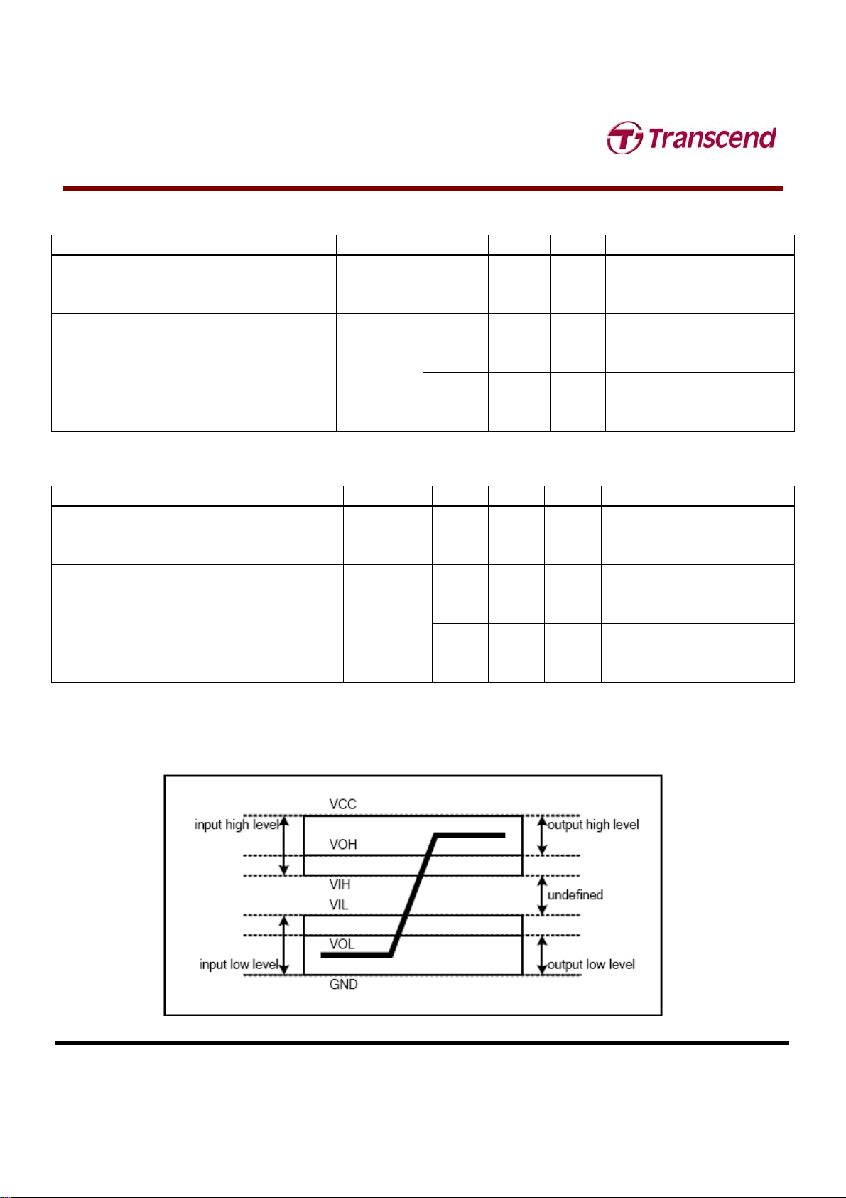
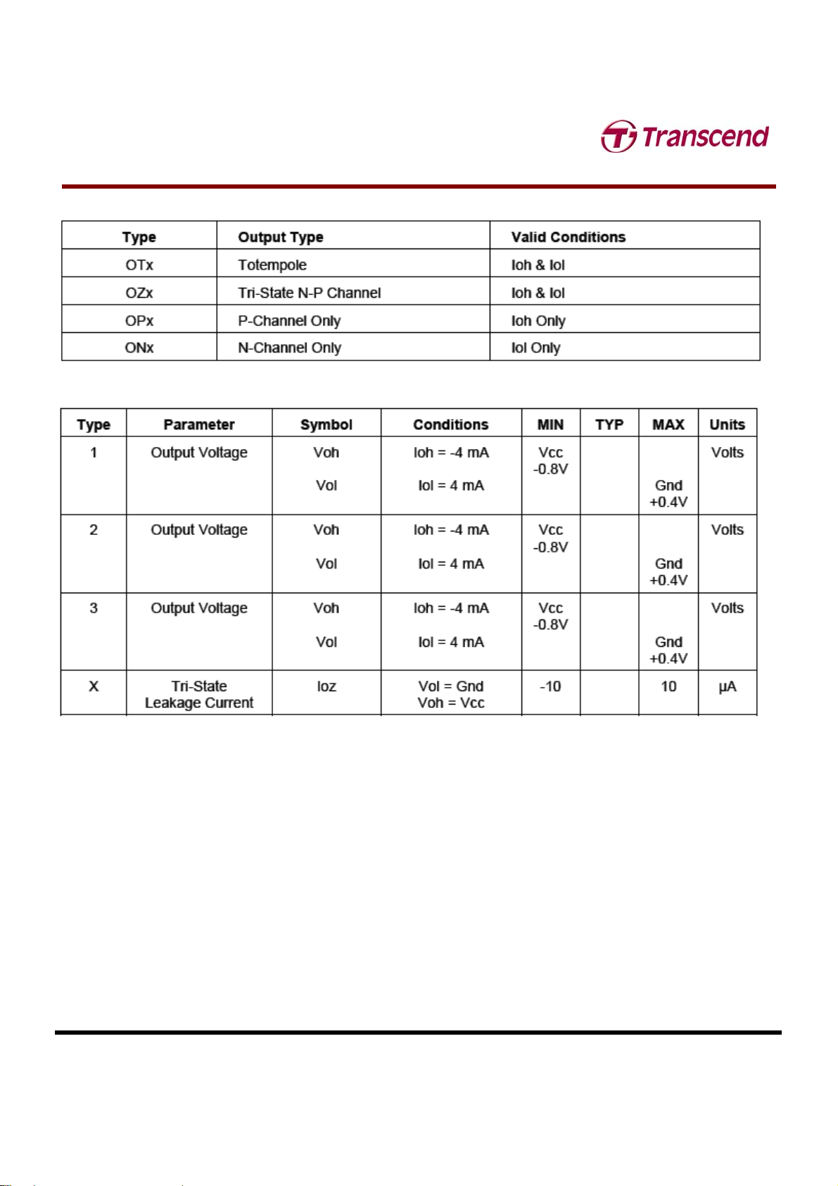
3.3.3 Output Drive Type
3.3.4 Output Drive Characteristics
T
T
T
S
S
S
3
3
3
2
2
2
M
M
M
~
~
~
1
1
1
G
G
G
C
C
C
F
F
F
8
8
8
0
0
0
80X CompactFlash Card
Transcend Information Inc.
V1.7
16
3.4 Signal Interface
Electrical specifications shall be maintained to ensure data reliability.
Item Signal Card
10
Host
10
Control Signal
-CE1
-CE2
-REG
-IORD
-IOWR
Pull-up to V
CC
500 KΩ≧ R≧ 50 KΩ and
shall be sufficient to keep inputs inactive
when the pins are not connected at the
host.
1
-OE
-WE
Pull-up to V
CC
500 KΩ ≧ R ≧ 50 KΩ .
1,2
RESET
Pull-up to V
CC
500 KΩ ≧ R ≧ 50 KΩ .
1,2,9,
Status Signal
READY
-WAIT
WP
Pull-up to V
CC
R ≧ 10 KΩ .
3
-INPACK
In PCMCIA PC Card modes Pull-up to V
CC
R ≧ 10 KΩ .
4
In True IDE mode, if DMA operation is
supported by the host, Pull-down to Gnd R
≧ 5.6 KΩ .
5
PC Card / True IDE hosts switch the pull-up
to pull down in True IDE mode if DMA
operation is supported.
The PC Card mode Pull-up may be left
active during True IDE mode if True IDE
DMA operation is not supported.
Address
A[10:00]
-CSEL
Data Bus D[15:00]
1.
Card Detect -CD[2:1] Connected to GND in the card
Voltage Sense
-VS1
-VS2
Pull-up to Vcc 10 KΩ ≦ R ≦ 100KΩ .
Battery/Detect BVD[2:1]
Pull-up R ≧ 50 KΩ .
3.6
Notes: 1) Control Signals: each card shall present a load to the socket no larger than 50 pF 10 at a DC current of 700 μ A low
state and 150 μ A high state, including pull-resistor. The socket shall be able to drive at least the following load
10
while meeting all AC timing requirements: (the number of sockets wired in parallel) multiplied by (50 pF with DC
current 700 μ A low state and 150 μ A high state per socket).
2) Resistor is optional.
3) Status Signals: the socket shall present a load to the card no larger than 50 pF
10 at a DC current of 400 μ A low state
and 100 μ A high state, including pull-up resistor. The card shall be able to drive at least the following load
10 while
meeting all AC timing requirements: 50 pF at a DC current of 400 μ A low state and 100 μ A high state.
4) Status Signals: the socket shall present a load to the card no larger than 50 pF
10 at a DC current of 400 μ A low state
and 100 μ A high state, including pull-up resistor. The card shall be able to drive at least the following load
10 while

T
T
T
S
S
S
3
3
3
2
2
2
M
M
M
~
~
~
1
1
1
G
G
G
C
C
C
F
F
F
8
8
8
0
0
0
80X CompactFlash Card
Transcend Information Inc.
V1.7
17
meeting all AC timing requirements: 50 pF at a DC current of 400 μ A low state and 100 μ A high state.
5) Status Signals: the socket shall present a load to the card no larger than 50 pF
10 at a DC current of 400 μ A low state
and 100 μ A high state, including pull-up resistor. The card shall be able to drive at least the following load
10 while
meeting all AC timing requirements: 50 pF at a DC current of 400 μ A low state and 1100 μ A high state.
6) BVD2 was not defined in the JEIDA 3.0 release. Systems fully supporting JEIDA release 3 SRAM cards shall pull-up
pin 45 (BVD2) to avoid sensing their batteries as “Low.”
7) Address Signals: each card shall present a load of no more than 100pF
10 at a DC current of 450μ A low state and
150μ A high state. The host shall be able to drive at least the following load
10 while meeting all AC timing
requirements: (the number of sockets wired in parallel) multiplied by (100pF with DC current 450μ A low state and
150μ A high state per socket).
8) Data Signals: the host and each card shall present a load no larger than 50pF
10 at a DC current of 450μ A and 150
μ A high state. The host and each card shall be able to drive at least the following load
10 while meeting all AC timing
requirements: 100pF with DC current 1.6mA low state and 300μ A high state. This permits the host to wire two
sockets in parallel without derating the card access speeds.
9) Reset Signal: This signal is pulled up to prevent the input from floating when a CFA to PCMCIA adapter is used in a
PCMCIA revision 1 host. However, to minimize DC current drain through the pull-up resistor in normal operation the
pull-up should be turned off once the Reset signal has been actively driven low by the host. Consequently, the input
is specified as an I2Z because the resistor is not necessarily detectable in the input current leakage test.

T
T
T
S
S
S
3
3
3
2
2
2
M
M
M
~
~
~
1
1
1
G
G
G
C
C
C
F
F
F
8
8
8
0
0
0
80X CompactFlash Card
Transcend Information Inc.
V1.7
18
3.5 Attribute Memory Read Timing
Figure: Attribute Memory Read Timing Diagram

T
T
T
S
S
S
3
3
3
2
2
2
M
M
M
~
~
~
1
1
1
G
G
G
C
C
C
F
F
F
8
8
8
0
0
0
80X CompactFlash Card
Transcend Information Inc.
V1.7
19
3.6 Configuration Register (Attribute Memory) Write Timing
Figure: Configuration Register (Attribute Memory) Write Timing Diagram
T
T
T
S
S
S
3
3
3
2
2
2
M
M
M
~
~
~
1
1
1
G
G
G
C
C
C
F
F
F
8
8
8
0
0
0
80X CompactFlash Card
Transcend Information Inc.
V1.7
20
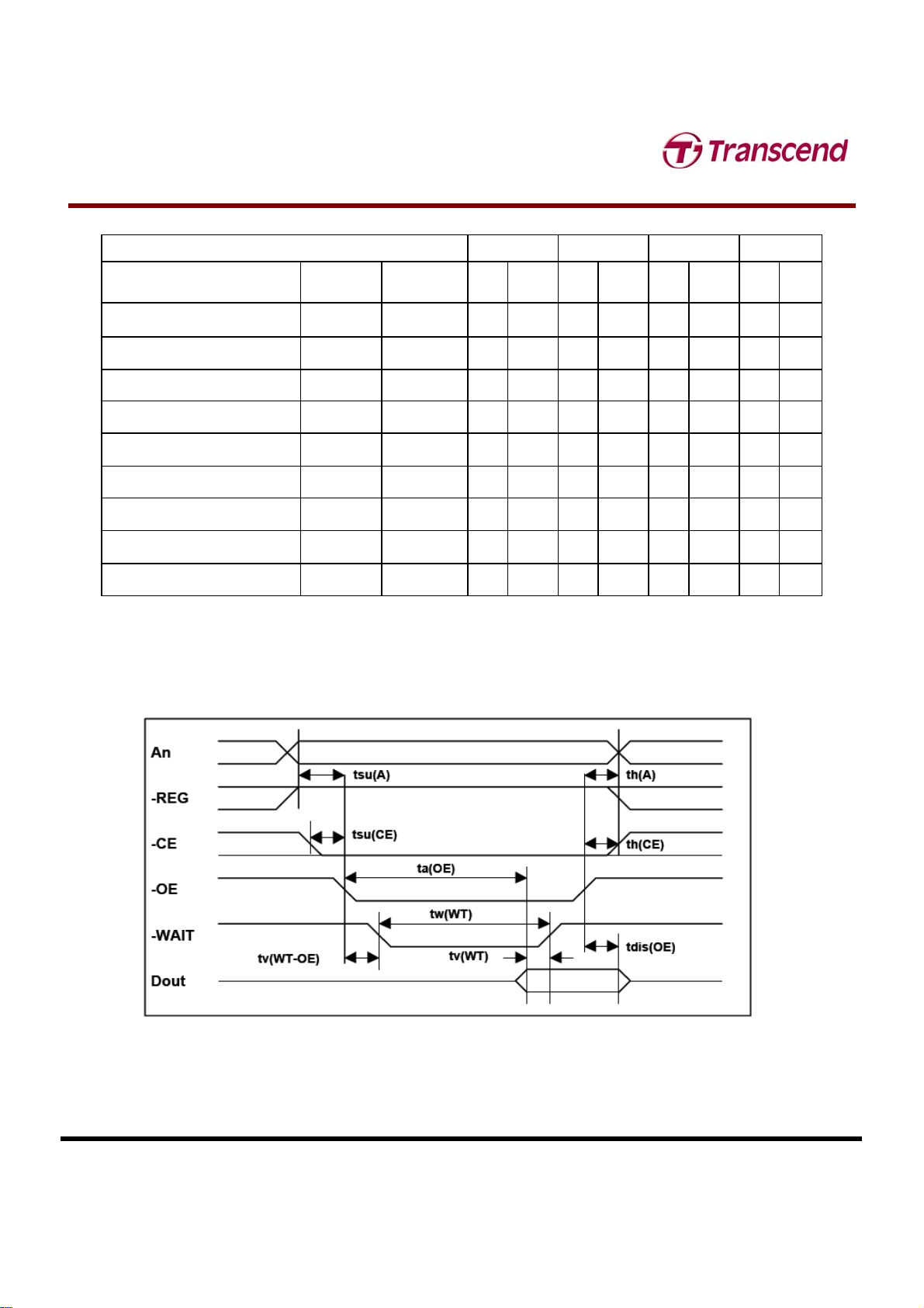
3.7 Common Memory Read Timing Specification
Cycle Time Mode: 250 ns 120 ns 100 ns 80 ns
Item Symbol
IEEE
Symbol
Min
ns.
Max
ns.
Min
ns.
Max
ns.
Min
ns.
Max
ns.
Min
ns.
Max
ns.
Output Enable Access Time ta(OE) tGLQV
125
60
50
45
Output Disable Time from OE tdis(OE) tGHQZ
100
60
50
45
Address Setup Time tsu(A) tAVGL 30
15
10
10
Address Hold Time th(A) tGHAX 20
15
15
10
CE Setup before OE tsu(CE) tELGL 0
0
0
0
CE Hold following OE th(CE) tGHEH 20
15
15
10
Wait Delay Falling from OE
tv(WT-OE
)
tGLWTV
35
35
35
na
1
Data Setup for Wait Release tv(WT) tQVWTH
0
0
0
na
1
Wait Width Time2 tw(WT) tWTLWTH
350
350
350
na
1
Notes:1) –WAIT is not supported in this mode.
2) The maximum load on -WAIT is 1 LSTTL with 50 pF (40pF below 120nsec Cycle Time) total load. All times are in nanoseconds.
Dout signifies data provided by the CompactFlash Storage Card to the system. The -WAIT signal may be ignored if the -OE cycle
to cycle time is greater than the Wait Width time. The Max Wait Width time can be determined from the Card Information
Structure. The Wait Width time meets the PCMCIA PC Card specification of 12µs but is intentionally less in this specification.
T
T
T
S
S
S
3
3
3
2
2
2
M
M
M
~
~
~
1
1
1
G
G
G
C
C
C
F
F
F
8
8
8
0
0
0
80X CompactFlash Card
Transcend Information Inc.
V1.7
21
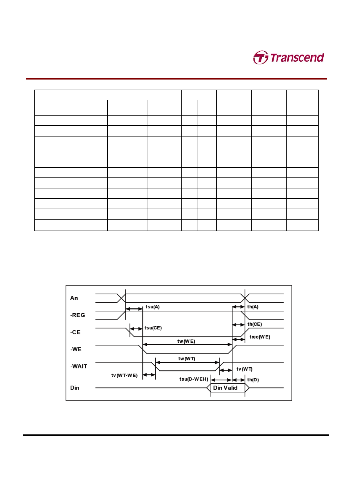
3.8 Common Memory Write Timing Specification
Cycle Time Mode: 250 ns 120 ns 100 ns 80 ns
Item Symbol
IEEE
Symbol
Min
ns.
Max
ns.
Min
ns.
Max
ns.
Min
ns.
Max
ns.
Min
ns.
Max
ns.
Data Setup before WE tsu (D-WEH) tDVWH 80
50
40
30
Data Hold following WE th(D) tWMDX 30
15
10
10
WE Pulse Width tw(WE) tWLWH 150
70
60
55
Address Setup Time tsu(A) tAVWL 30
15
10
10
CE Setup before WE tsu(CE) tELWL 0
0
0
0
Write Recovery Time trec(WE) tWMAX 30
15
15
15
Address Hold Time th(A) tGHAX 20
15
15
15
CE Hold following WE th(CE) tGHEH 20
15
15
10
Wait Delay Falling from WE tv (WT-WE) tWLWTV
35
35
35
na
1
WE High from Wait Release tv(WT) tWTHWH 0
0
0
na
1
Wait Width Time2 tw (WT) tWTLWTH
350
350
350
na
1
Notes: 1) –WAIT is not supported in this mode.
2) The maximum load on -WAIT is 1 LSTTL with 50 pF (40pF below 120nsec Cycle Time) total load. All times are in
nanoseconds. Din signifies data provided by the system to the CompactFlash Storage Card. The -WAIT signal may be
ignored if the -WE cycle to cycle time is greater than the Wait Width time. The Max Wait Width time can be determined from
the Card Information Structure. The Wait Width time meets the PCMCIA PC Card specification of 12μs but is intentionally
less in this specification.

T
T
T
S
S
S
3
3
3
2
2
2
M
M
M
~
~
~
1
1
1
G
G
G
C
C
C
F
F
F
8
8
8
0
0
0
80X CompactFlash Card
Transcend Information Inc.
V1.7
22
3.9 I/O Input (Read) Timing Specification
Cycle Time Mode: 250 ns 120 ns 100 ns 80 ns
Item Symbol
IEEE
Symbol
Min
ns.
Max
ns.
Min
ns.
Max
ns.
Min
ns.
Max
ns.
Min
ns.
Max
ns.
Data Delay after IORD td(IORD) tlGLQV
100
50
50
45
Data Hold following IORD th(IORD) tlGHQX 0
5
5
5
IORD Width Time tw(IORD) tlGLIGH 165
70
65
55
Address Setup before IORD tsuA(IORD) tAVIGL 70
25
25
15
Address Hold following IORD thA(IORD) tlGHAX 20
10
10
10
CE Setup before IORD tsuCE(IORD) tELIGL 5
5
5
5
CE Hold following IORD thCE(IORD) tlGHEH 20
10
10
10
REG Setup before IORD tsuREG (IORD) tRGLIGL 5
5
5
5
REG Hold following IORD thREG (IORD) tlGHRGH 0
0
0
0
INPACK Delay Falling from IORD
3
tdfINPACK (IORD) tlGLIAL 0 45 0 na
1
0 na
1
0 na
1
INPACK Delay Rising from IORD
3
tdrINPACK (IORD) tlGHIAH
45
na
1
na
1
na
1
IOIS16 Delay Falling from Address
3
tdfIOIS16 (ADR) tAVISL
35
na
1
na
1
na
1
IOIS16 Delay Rising from Address
3
tdrIOIS16 (ADR) tAVISH
35
na
1
na
1
na
1
Wait Delay Falling from IORD
3
tdWT(IORD) tlGLWTL
35
35 35 na
2
Data Delay from Wait Rising
3
td(WT) tWTHQV
0
0 0 na
2
Wait Width Time3 tw(WT) tWTLWTH
350
350 350 na
2
T
T
T
S
S
S
3
3
3
2
2
2
M
M
M
~
~
~
1
1
1
G
G
G
C
C
C
F
F
F
8
8
8
0
0
0
80X CompactFlash Card
Transcend Information Inc.
V1.7
23
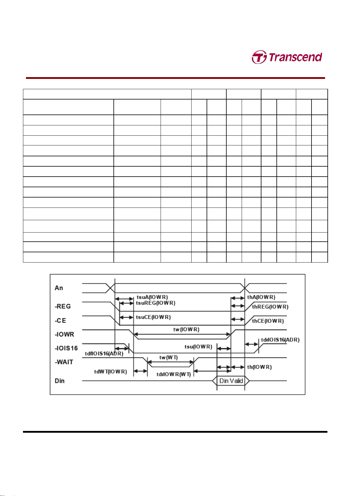
3.10 I/O Output (Write) Timing Specification
Cycle Time Mode: 255 ns 120 ns 100 ns 80 ns
Item Symbol
IEEE
Symbol
Min
ns.
Max
ns.
Min
ns.
Max
ns.
Min
ns.
Max
ns.
Min
ns.
Max
ns.
Data Setup before IOWR tsu(IOWR) tDVIWH 60 20 20 15
Data Hold following IOWR th(IOWR) tlWHDX 30 10 5 5
IOWR Width Time tw(IOWR) tlWLIWH 165 70 65 55
Address Setup before IOWR tsuA(IOWR) tAVIWL 70 25 25 15
Address Hold following IOWR thA(IOWR) tlWHAX 20 20 10 10
CE Setup before IOWR tsuCE (IOWR) tELIWL 5 5 5 5
CE Hold following IOWR thCE (IOWR) tlWHEH 20 20 10 10
REG Setup before IOWR tsuREG (IOWR) tRGLIWL 5 5 5 5
REG Hold following IOWR thREG (IOWR) tlWHRGH 0 0 0 0
IOIS16 Delay Falling from Address
3
tdfIOIS16 (ADR) tAVISL 35 na
1
na
1
na
1
IOIS16 Delay Rising from Address
3
tdrIOIS16 (ADR) tAVISH 35 na
1
na
1
na
1
Wait Delay Falling from IOWR
3
tdWT(IOWR) tlWLWTL 35 35 35 na
2
IOWR high from Wait high
3
tdrIOWR (WT) tWTJIWH 0 0 0 na
2
Wait Width Time
3
tw(WT) tWTLWTH 350 350 350 na
2

T
T
T
S
S
S
3
3
3
2
2
2
M
M
M
~
~
~
1
1
1
G
G
G
C
C
C
F
F
F
8
8
8
0
0
0
80X CompactFlash Card
Transcend Information Inc.
V1.7
24
3.11 True IDE PIO Mode Read/Write Timing Specification
Mode
Item
0 1 2 3 4 5 6
Note
t0 Cycle time (min) 600 383 240 180 120 100 80 1
t1
Address Valid to -IORD/-IOWR
setup (min)
70 50 30 30 25 15 10
t2 -IORD/-IOWR (min) 165 125 100 80 70 65 55 1
t2 -IORD/-IOWR (min) Register (8 bit) 290 290 290 80 70 65 55 1
t2i -IORD/-IOWR recovery time (min) - - - 70 25 25 20 1
t3 -IOWR data setup (min) 60 45 30 30 20 20 15
t4 -IOWR data hold (min) 30 20 15 10 10 5 5
t5 -IORD data setup (min) 50 35 20 20 20 15 10
t6 -IORD data hold (min) 5 5 5 5 5 5 5
T6Z -IORD data tristate (max) 30 30 30 30 30 20 20 2
t7
Address valid to -IOCS16 assertion
(max)
90 50 40 n/a n/a n/a n/a 4
t8
Address valid to -IOCS16 released
(max)
60 45 30 n/a n/a n/a n/a 4
t9 -IORD/-IOWR to address valid hold 20 15 10 10 10 10 10
tRD
Read Data Valid to IORDY active
(min), if IORDY initially low after tA
0 0 0 0 0 0 0
tA IORDY Setup time 35 35 35 35 35 na
5
na
5
3
tB IORDY Pulse Width (max) 1250 1250 1250 1250 1250 na
5
na
5
tC IORDY assertion to release (max) 5 5 5 5 5 na
5
na
5
Notes: All timings are in nanoseconds. The maximum load on -IOCS16 is 1 LSTTL with a 50 pF (40pF below 120nsec Cycle Time) total
load. All times are in nanoseconds. Minimum time from -IORDY high to -IORD high is 0 nsec, but minimum -IORD width shall still
be met.
1) t0 is the minimum total cycle time, t2 is the minimum command active time, and t2i is the minimum command recovery time or
command inactive time. The actual cycle time equals the sum of the actual command active time and the actual command
inactive time. The three timing requirements of t0, t2, and t2i shall be met. The minimum total cycle time requirement is greater
than the sum of t2 and t2i. This means a host implementation can lengthen either or both t2 or t2i to ensure that t0 is equal to
or greater than the value reported in the device’s identify device data. A CompactFlash Storage Card implementation shall
support any legal host implementation.
2) This parameter specifies the time from the negation edge of -IORD to the time that the data bus is no longer driven by the
CompactFlash Storage Card (tri-state).
3) The delay from the activation of -IORD or -IOWR until the state of IORDY is first sampled. If IORDY is inactive then the host
shall wait until IORDY is active before the PIO cycle can be completed. If the CompactFlash Storage Card is not driving IORDY
negated at tA after the activation of -IORD or -IOWR, then t5 shall be met and tRD is not applicable. If the CompactFlash
Storage Card is driving IORDY negated at the time tA after the activation of -IORD or -IOWR, then tRD shall be met and t5 is
not applicable.
4) t7 and t8 apply only to modes 0, 1 and 2. For other modes, this signal is not valid.
5) IORDY is not supported in this mode.

T
T
T
S
S
S
3
3
3
2
2
2
M
M
M
~
~
~
1
1
1
G
G
G
C
C
C
F
F
F
8
8
8
0
0
0
80X CompactFlash Card
Transcend Information Inc.
V1.7
25
 Loading...