


 Loading...
Toshiba TP43H60, TP43H95, TP50H15, TP50H50, TP50H60 Service Manual
...Projection Televisions
Main Power Supply
&
Complete Shutdown Troubleshooting Guide
TP43H60 TP55H64
TP43H95 TP55H95
TP50H15 TP61H60
TP50H50 TZ43V61
TP50H60 TZ50V51
TP50H64 TZ50V61
TP50H95 TZ55V61
TP55H60 TZ61V61
Contents |
|
Main Power Supply |
................. 3 |
Overall Block Diagram ................................................................................................. |
4 |
Operation ...................................................................................................................... |
5 |
Surge Protection Relay. ............................................................................................... |
6 |
Start-up and Over Voltage Protect .............................................................................. |
6 |
Logic and Drivers ......................................................................................................... |
7 |
Oscillator ....................................................................................................................... |
7 |
Oscillator Control ......................................................................................................... |
8 |
Latch .............................................................................................................................. |
8 |
Thermal Shock Detection Block ................................................................................. |
8 |
Over Current Protection .............................................................................................. |
8 |
Soft Start ....................................................................................................................... |
9 |
Resonate Correction .................................................................................................... |
9 |
Additional Information on Q801 ................................................................................ |
10 |
Block Diagram of Q801 ............................................................................................. |
11 |
Troubleshooting Flowchart ....................................................................................... |
12 |
Shutdown Guide .................... |
14 |
Summary of Shutdown Circuits. ............................................................................... |
15 |
Peak-Response Meter. ............................................................................................... |
16 |
No Peak-Response Meter. ......................................................................................... |
16 |
Monitoring Circuits .................................................................................................... |
17 |
X-Ray Protect. ............................................................................................................. |
17 |
+125V Over Current Protect. ..................................................................................... |
18 |
+36V Over Current Protect. ....................................................................................... |
19 |
+18V and – 18V Over Current Protect. ..................................................................... |
20 |
+35V Over Current Protect. ....................................................................................... |
20 |
+ 9V Under Voltage Protect ....................................................................................... |
21 |
+ 35 Under Voltage Protect ........................................................................................ |
21 |
200V Under Voltage Protect. ..................................................................................... |
21 |
Troubleshooting Flowchart ....................................................................................... |
22 |
Main Power Supply
3

Overall Block Diagram
Figure 1 is the overall block diagram of the main switching power supply and the standby power supply. The standby supply is always active when the television is plugged into an AC line source. This supply delivers a 5V VDD and a reset 5V to the microprocessor to keep the microprocessor functioning at all times, even when the television is not operating. Transformer T840 isolates the standby supply from the live ground, and D840 is a full-wave bridge rectifier that supplies 12Vdc to voltage regulator Q840 and relay SR81 (connection not shown). When the microprocessor receives an ON command from the remote control or power key, on the front of the television, it sends 5V to relay drivers
Stand-By Supply
QB30 and Q843 to close relay SR81.
When the relay closes, the AC line input is applied directly to the main power supply. The supply starts to operate and turns ON the television. D801 is the fullwave bridge rectifier for the main power supply. It rectifies the 120V AC line input to 165Vdc and applies it to the main switching IC, Q801. The primary side of the power supply is not isolated and, therefore, is at live ground. Detailed explanations of the main power supply are covered in the remainder of this section.
Troubleshooting Tip:
If SR81 never closes, check the standby power supply. Both the 5V VDD and the reset 5V are mandatory for the microprocessor to operate.
Rectifier & |
Stand-by |
|
Isolation Trans. |
Regulator |
Microprocessor |
Main Power Supply
D840 |
|
+5-1 |
5V |
VDD |
|
Q840 |
|
5V |
|
|
|
T840 |
|
Reset |
|
||
|
|
|
|||
|
|
|
|
QA01 |
11 |
5V=Relay On |
|
|
|
||
|
|
|
|
||
0V=Relay Off |
|
|
|
9 |
|
|
|
|
|
|
|
|
From Shutdown |
|
|
||
QB30 |
Relay Drivers |
|
|
9 |
|
Q843 |
|
|
|
|
10 |
|
Rectifier |
Main Switching IC |
|||
|
|
|
|
|
|
SR81 |
D801 |
165V |
Q801 |
4 |
12 |
|
|
|
|||
AC Line |
Relay |
|
13 |
|
|
||
Input |
|
7 |
|
|
|
|
|
|
|
|
14 |
|
|
C870 |
15 |
|
|
|
|
|
|
|
16 |
|
|
|
17 |
|
|
T862 |
|
Photo
Coupler
Feedback
Q862
Q760 |
30V |
To Q752 |
Reg. |
Conv. Output |
|
Rectifiers |
|
|
|
|
|
To Q752 & Q751 |
D856 +36 |
|
Conv. Outputs |
|
D855 |
|
Q754 |
5V |
To Digital Conv. PC, |
|
|
Reg. |
Q764 & Q767 |
|||
D851 |
+18 |
Q755 |
9V |
To Q752 |
|
|
Reg. |
Conv. Output |
|||
D854 |
-18 |
|
|
To Q752 & Q751 |
|
|
|
|
|||
|
|
|
Conv. Outputs |
||
|
|
|
-9V |
||
|
|
Q756 |
To Digital Conv. PC, |
||
D886 |
+38 |
Reg. |
|||
|
|
||||
|
|
To Q601 Audio Out |
|||
D889 |
|
|
|
||
|
|
9V |
To Q501 |
||
|
|
Q430 |
|||
|
|
Reg. |
Horizontal Start-up |
||
|
|
|
|||
D891 |
+12 |
|
|
To Shutdown & Surge protect: |
|
D894 |
|
|
9V |
Q846,SR82,Q757, & Q758 |
|
|
Q832 |
+9-2 To Numerous Circuits |
|||
|
|
Reg. |
|||
|
|
|
|
||
D882 |
+125 |
Q830 |
5V&9V |
+5-2 To Numerous Circuits |
|
|
|
Reg. |
+9-1 To Numerous Circuits |
||
|
|
|
|||
D884 |
|
|
5V |
|
|
|
|
Q831 |
+5-3 To PIP Module & QBB3 |
||
|
|
Reg. |
|||
|
|
|
|
||
Error |
|
|
|
To Horizontal Output |
|
|
|
32V |
|
||
Amp. |
|
D101 |
To Tuner(s) |
||
|
Z801 |
Reg. |
|||
|
|
Reg.= Regulator |
|||
|
|
|
|||
|
|
|
|
||
|
|
|
|
Conv.= Convergence |
Figure 1
4

Operation
The main power supply is a current resonance switching power supply. Figure 2 is a basic block diagram for this supply. The primary winding of T862 and capacitor C870 create a LC series resonant circuit. An oscillator (OSC), drive circuit, and two MOSFETs are located internal to Q801 (STR-Z4117). The OSC determines the power supply’s switching frequency. The drive circuit alternately switches the MOSFETs ON and OFF. The two power MOSFETs, in a push-pull configuration, alternate the current flow through the LC circuit during normal operation. The alternating current continually builds and collapses an electromagnetic field around T862’s primary windings. The collapsing of the electromagnetic field induces current into the secondary windings of T862. A full-wave bridge rectifier converts the induced current into 125Vdc.
To regulate the 125Vdc, an error amplifier monitors the voltage and supplies a negative feedback to the oscillator through photo-coupler Q862. Q862 isolates
O |
D |
|
r |
||
S |
i |
|
C |
v |
|
e |
||
|
||
|
Q801 |
T862 125V+B
C870 |
Error |
|
|
Photo |
Amp |
|
|
Coupler |
Z801 |
Q862 |
|
Figure 2
the primary side of the power supply from the secondary side.
Refer to figure 3. The power supply’s switching frequency operates above the LC resonance frequency. When the load increases and requires more current, the oscillator frequency decreases and operates closer to the LC resonant frequency. The closer the switch-
ing frequency is to resonance, the more current flows through the primary windings of T862 and the larger the electromagnetic field builds. The larger the electromagnetic field is when it collapses, the more current is induced in the secondary winding. When the load decreases and requires less current, the switching frequency increases and moves away from resonance. As a result, less current is induced in the secondary windings.
Load |
Increased |
|
|
Current |
Load |
|
|
|
|
|
Decreased |
|
|
|
Load |
|
ResonantOperating |
Switching |
|
|
Freq. |
||
|
|
||
|
Freq |
Freq |
|
|
. |
. |
|
|
|
||
Normal Operatin Freqency is 70-80kHz
Figure 3
5

Surge Protection Relay. |
Start-up and Over Voltage Protect |
|||||||||||||
Refer to figure 4. To prolong the life of the power |
Refer to figure 5. The positive cycle of the AC line |
|||||||||||||
supply, a surge circuit reduces current through the main |
input supplies a 16V start-up pulse to pin 8 of Q801 |
|||||||||||||
power supply at startup. When the television is OFF, |
via resistor R861. After start-up, a drive circuit con- |
|||||||||||||
relays SR81 and SR82 are open. At turn ON, SR81 |
sisting of a secondary winding of T862, diode D864, |
|||||||||||||
closes and the switching power supply begins to oper- |
and capacitor C868 supply 16-20Vdc to pin 8 of Q801 |
|||||||||||||
ate. During this time, the power supply draws a large |
to maintain its operation. The voltage developed by |
|||||||||||||
amount of current. To reduce the current, the ground |
the drive circuit fluctuates with the switching frequency |
|||||||||||||
path for bridge rectifier D801 is through resistor R810. |
of the power supply. Therefore, the voltage on pin 8 is |
|||||||||||||
Once the power supply becomes fully operational and |
also applied to an over voltage protect (OVP) block |
|||||||||||||
produces output voltages, one of these voltages is ap- |
internal to Q801. If the voltage on pin 8 increases to |
|||||||||||||
plied to the base of transistor Q846. This voltage turns |
25V, the OVP triggers the latch and switching stops. |
|||||||||||||
Q846 ON and allows current to flow through the coil |
Refer to the latch block for further information. D876 |
|||||||||||||
of SR82. SR82’s switch closes and creates a direct |
is a 27V zener diode that protects Q801 by preventing |
|||||||||||||
ground path for D801 by bypassing R810. SR82 re- |
excess voltage increases on pin 8. |
|
|
|
|
|
|
|
||||||
mains closed during normal operation. |
|
|
|
|
|
|
|
|
|
|
|
|
|
|
Troubleshooting Tip: |
R861 |
|
D864 |
R871 |
||||||||||
|
|
|
||||||||||||
R810 is a fusible resistor. If SR82 does not close after |
|
|||||||||||||
|
|
|
|
|
|
|
|
|
|
|
|
|
||
the power supply is fully operational, R810 eventually |
From |
|
|
|
|
|
T862 |
|||||||
|
|
|
|
|
||||||||||
opens and prevents the power supply from operating. |
D876 |
|
|
|||||||||||
D801 |
|
|
||||||||||||
|
|
|||||||||||||
|
|
|
|
|
|
|
|
|
|
|
||||
Whenever troubleshooting the power supply, check R810 |
|
|
|
|
C868 |
|
||||||||
|
|
|
|
|
||||||||||
first. If R810 is open, replace it using Toshiba part num- |
16-20 Vdc |
8 Vcc |
|
|
|
|
|
|
|
|||||
ber 24007061 and look for cold solders around Q846 |
|
|
|
|
|
|
|
|||||||
|
|
|
|
|
|
|
|
|||||||
|
Q801 |
|
|
|
|
|
|
|
||||||
and R846. |
|
|
|
|
|
|
|
|
||||||
|
|
|
|
|
|
|
|
|
|
|
|
|
||
OVP |
Start |
Main Power Supply |
|
||
Relay |
|
Figure 5 |
|
Q801 |
125V |
||
SR81 |
|||
|
|||
D801 |
and |
12V |
|
|
T862 |
|
|
SR82
R846
R810
Q846
Figure 4
6
Logic and Drivers
Refer to figure 6. The logic block controls the MOSFETs’ switching frequency. The outputs of the logic block feed two drivers that are powered by the start block. After the start-up voltage is applied to pin 8, the start block supplies a drive Vcc (DRI Vcc) of approximately 8V to pin 9. Delaying the driver supplies at start-up, prevents damaging the MOSFETs. The 8V on pin 9 powers driver B internally. To power driver A, resistor R862 and diode D862 add the voltage from pin 9 to the voltage on pin 15. D875, C863, D873 and C873 are voltage regulators and filters for these supplies.
D873 |
|
|
|
C873 |
R862 |
D862 |
|
|
|
||
|
DRI Vcc |
VB |
D875 |
8 Vcc |
C863 |
||
9 |
15 |
|
|
|
|
Q801 |
VIN |
|
|
|
|
|
1 |
Start |
|
B+ |
|
130V |
|
|
|
|
|
|
A |
|
Logic |
Out |
|
14 |
|
|
To |
|
|
|
|
|
|
T862 |
|
|
B |
|
|
COM. |
|
|
12 |
Figure 6
Oscillator
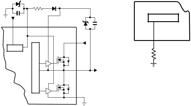
Refer to figure 7. Q801’s internal Oscillator develops the power supply’s switching frequency by generating a ramp waveform internally. During normal operation, both MOSFETs are OFF for a short time when they are alternately switching. This OFF time is called dead time and determined by resistor R867 on the dead time (DT) terminal pin 7.
Q801
OSC
7 DT
R867
Figure 7
7
Loading...