


 Loading...
Toshiba TN50X81, TN55X71, TN55X81, TN61X81, TN40X81 User Manual
...NTDMOD05
TOSHIBA
Service Training
PROJECTION
TELEVISIONS
Main Power Supply
& Complete
Shutdown Guide
TN50X81
TN55X71
TN55X81
TN61X81
TN40X81
TW56X81
TW65X81
Copyright 1999
TOSHIBA AMERICA CONSUMER PRODUCTS, INC. NATIONAL SERVICE DIVISION
1420-B TOSHIBA DRIVE, LEBANON, TN 37087
Contents |
|
Overall Block Diagram |
......... 5 |
Overall Block Diagram ..................................................................................... |
6 |
Main Power Supply .............. |
7 |
Main Power Supply ........................................................................................... |
8 |
VIN Terminal (pin 5) - Start Circuit ................................................................... |
9 |
OCP/INH Terminal (pin 4) Function ................................................................. |
9 |
Soft Start ........................................................................................................... |
10 |
Surge Protect. .................................................................................................. |
11 |
Oscillator/Constant Voltage Control Circuit ................................................ |
12 |
Latch Block ...................................................................................................... |
13 |
Overheat Protection Block (Internal to Q801) ............................................. |
13 |
Overvoltage Protection Block (Pin 5) ........................................................... |
13 |
Latch Trigger Terminal (Pin 7)....................................................................... |
13 |
Troubleshooting Flowchart ........................................................................... |
14 |
Sub Power Supply .............. |
15 |
Operation.......................................................................................................... |
16 |
Start-up and Over Voltage Protect ................................................................ |
17 |
Logic and Drivers............................................................................................ |
18 |
Oscillator .......................................................................................................... |
18 |
Oscillator Control ............................................................................................ |
19 |
Latch ................................................................................................................. |
19 |
Thermal Shock Detection Block ................................................................... |
20 |
Over Current Protection................................................................................. |
20 |
Soft Start ........................................................................................................... |
20 |
Resonance Correction ................................................................................... |
21 |
Additional Information .................................................................................... |
22 |
Troubleshooting Flowcharts ......................................................................... |
23 |
Shutdown ......................................................................................................... |
25 |
Basic Operation ............................................................................................... |
26 |
||
Monitoring Circuits ......................................................................................... |
28 |
||
X-Ray Protection ............................................................................................. |
28 |
||
+128V |
Over Current Protect .......................................................................... |
29 |
|
+128V |
Over Voltage Protect ........................................................................... |
30 |
|
Horizontal Stop Protection Circuit ................................................................ |
31 |
||
+21V |
Over Voltage Protect ............................................................................. |
32 |
|
+35V |
Over Current Protect ............................................................................ |
33 |
|
+21V |
Over Current Protect ............................................................................ |
34 |
|
-21V Over Current Protection ........................................................................ |
35 |
||
+200V |
Low Voltage Protect ............................................................................ |
36 |
|
Troubleshooting Flowchart ........................................................................... |
37 |
||
Overall Block Diagram
5

Overall Block Diagram
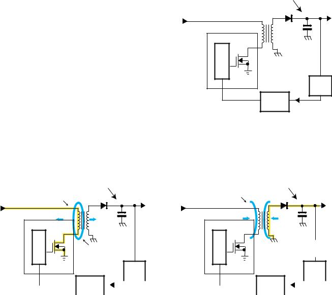
Figure 1 is an overall block diagram of the standby, main, and sub power supplies in the progressive scan televisions. The standby supply is always active whenever the television is plugged into an AC line source. It delivers 5V VDD and a reset 5V to the microprocessor to keep it operational at all times, even when the television is OFF. Transformer T840 isolates the standby supply from the live ground, and D840 is a full-wave bridge rectifier that supplies 15V DC to voltage regulator Q840 and relays SR81 and SR83 (relay connections not shown). When the microprocessor receives an ON command from the remote control or power key on the front of the television, it sends 5V to the relay drivers to close relays SR81 and SR83. Closing the relays supplies the AC line input to the remaining two power supplies to operate the television.
Troubleshooting Tip:
If both relays never close, check the standby power supply. Both the 5V VDD and the reset 5V are mandatory for the microprocessor to operate.
The main power supply and sub power supply work independently from each other, so one supply can be disabled to check the other. If the main power supply is disabled, the television would not have picture or sound, but the microprocessor would still control the relays. Therefore, the sub supply could be turned ON and OFF and its voltages would appear as normal. If the sub power supply is disabled, everything would work except the picture would be out of convergence. Either power supply can easily be disabled by removing its fuse: F860 for the sub supply and F811 for the main supply.
Standby Supply
Rectifier & |
Standby |
|
|
|
Isolation Trans. |
Regulator |
Microprocessor |
||
|
+5-1 |
5V |
VDD |
|
D840 |
|
|
||
Q840 |
5V |
|
||
T840 |
Reset |
|||
|
||||
|
|
|
QA01 |
|
5V=Relay On |
|
|
||
0V=Relay Off |
|
|
||
|
|
|
Main Power Supply |
|
Q841 |
Relay |
|
|
|
Q842 |
Drivers |
|
|
|
|
|
|
Rectifier |
|
3 |
|
|
|
F811 |
|
|
|
SR81 |
|
140V |
|
|
|
|
D801 |
|
|
|
AC Line |
Relay |
|
|
|
2 |
Input |
|
|
|
|
|
|
|
Main Switching IC |
|
||
|
|
|
|
||
|
|
|
|
Q801 |
|
|
|
|
Feedback |
Photo |
|
|
|
|
|
|
Coupler |
|
5V=Relay On |
|
|
|
QB03 |
|
0V=Relay Off |
|
|
|
|
|
|
|
|
|
|
|
Relay |
Q844 |
|
|
|
|
Drivers |
Q843 |
|
|
|
|
|
|
Rectifier |
Main Switching IC |
|
|
|
|
|
|
|
|
|
SR83 |
F860 |
140V |
3 |
|
|
D861 |
Q888 |
|
|
|
|
Relay |
|
|
|
|
|
|
|
|
2 |
|
|
|
|
Feedback |
Photo |
|
Sub-Power Supply |
|
|
Coupler |
|
|
|
|
Q861 |
||
|
|
|
|
|
|
T861
|
+7V |
18 |
D811 |
|
19 |
+7V |
|
D813 |
21 |
|
20 |
|
|
+35V |
22 |
D812 |
|
|
|
+15V |
12 |
D810 |
|
|
|
+11V |
14 |
D809 |
|
|
15 |
|
16 |
+128V |
|
D808 |
17 |
|
Error
Amp.
Q804
9 |
|
|
17 |
D887 |
36.5V |
|
& |
|
|
D888 |
|
10 |
|
21V |
13 |
|
|
12 |
D891 |
|
|
D895 |
-21V |
T888 14
Error
Amp.
Q863
Figure 1. Overall Block Diagram
6
Main Power Supply
7
Main Power Supply
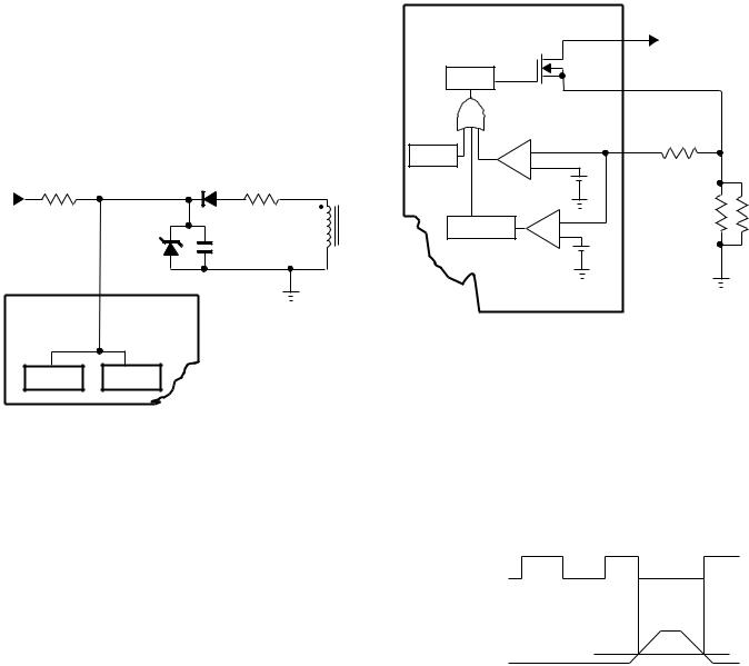
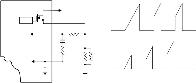
The main power supply is a ringing choke converter. Figure 2 is a block diagram for this supply. An oscillator (OSC) and a switching MOSFET are internal to the main switching IC, Q801. During normal operation, D801 rectifies the AC line input to approximately 140V. This voltage is applied to the MOSFET through transformer T861’s primary winding. As shown in Figure 3a, when the MOSFET conducts, current flows through T861’s primary windings and builds an electromagnetic field. Figure 3b demonstrates that after the field builds, the MOSFET opens to stop the current flow through T861. This causes the electromagnetic field to collapse and induce current into the secondary windings.
128V+B
140V dc
T861
From D801
D808
Q801
O
S
C
Error
Amp
Photo
Coupler Q804
QB03
Figure 2. Main Power Supply Block Diagram
When the MOSFET conducts, |
128V+B |
When the MOSFET Stops conducting, |
128V+B |
|||
|
the electromagnetic field collapses... |
|
||||
current flows through T862,... |
|
|
||||
T861 |
|
T861 |
||||
|
|
|
|
|||
140V dc |
|
|
D808 |
140V dc |
|
D808 |
|
|
|
|
|
||
From D801 |
Q801 |
|
|
From D801 |
Q801 |
|
|
|
|
|
|
||
|
O |
|
|
|
O |
|
|
S |
...and an electromagnetic |
|
S |
...and current is induced in |
|
|
C |
|
field builds. |
|
C |
the secondary windings. |
|
|
|
|
|||
|
|
|
Error |
|
|
Error |
|
|
|
Amp |
|
|
Amp |
|
|
Photo |
|
|
|
|
|
|
|
|
Photo |
|
|
|
|
|
|
|
|
|
|
|
|
|
|
|
|
|
|
|
|
||||
|
|
Coupler |
|
|
|
Q804 |
|
|
|
Coupler |
|
|
Q804 |
||||
|
|
QB03 |
|
|
|
|
|
|
QB03 |
|
|
|
|
|
|||
|
|
|
|
|
|
|
|
|
Electromagnetic Field |
|
|
|
|
|
|||
|
|
|
|
|
|
|
|
|
|
|
|
|
|
||||
|
|
|
|
|
|
|
|
|
|
|
|
|
|
||||
|
|
|
|
|
|
|
|
|
Current Flow |
|
|
|
|
|
|||
|
|
|
|
|
|
|
|
|
|
|
|
|
|
||||
|
|
|
|
|
|
|
|
|
|
|
|
|
|
||||
(a) |
|
|
|
|
(b) |
|
|
|
|
|
|||||||
Figure 3. Main Power Supply Operation
8
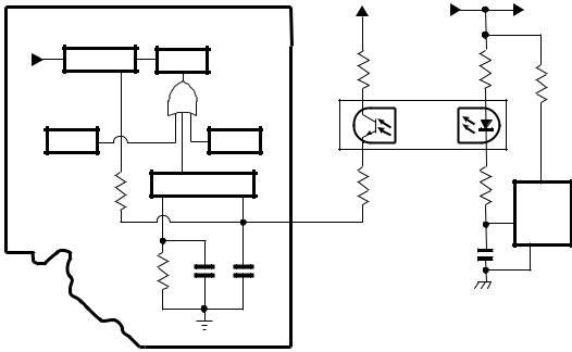
VIN Terminal (pin 5) - Start Circuit
As shown in Figure 4, pin 5 (VIN) of Q801 is the Startup and Over Voltage Protect (OVP) for Q801.
To start the operation of the power supply, 140V draws current through resistors R802 and R803 which builds a charge on capacitor C825. When the charge reaches 22.5V, Q801 starts switching. Once Q801 is operating normally, the ND winding and rectifier diode D805 provide 25V to pin 5 to maintain Q801’s switching operation. At this time, C825 functions as a filter capacitor.
Pin 5 is also the over voltage protection (OVP). If the voltage on VIN raises above 28V, an internal latch stops Q801 from operating. Refer to the Latch section for further details.
R803 & R802 |
D805 |
R825 |
T861 |
|
|
|
|
||
From |
|
|
|
ND |
D801 |
D806 |
C825 |
|
|
|
|
|||
25V dc 5 VIN
Q801
OVP Start
Figure 4. VIN Terminal and Start Circuit
OCP/INH Terminal (pin 4) Function
The OCP/INH terminal is a safety terminal that protects Q801 if an over current condition develops during operation. Figure 5 shows this circuit diagram.
(1)OCP Function (Over Current Protect)
When the MOSFET is turned ON, current flows through resistors R827 and R828 and a voltage develops at the over current protect (OCP) terminal at pin 4. If the voltage reaches 0.5V, the internal OCP comparator turns the MOSFET OFF and stops its current flow.
(2)INH Function (OFF Time Control)
At the same time the OCP comparator turns the MOSFET OFF, the inhibit (INH) comparator stops the oscillator and prevents the MOSFET and oscillator from operating until the OCP voltage drops below 0.5V. The waveforms for this operation are shown in Figure 6.
Q801 |
|
|
|
1 |
To T861 |
|
Drive |
|
|
2 |
|
|
OCP |
R807 |
Latch |
4 |
|
|
|
|
|
0.5V |
|
|
INH |
R827 |
|
R828 |
|
|
Oscillator |
|
|
|
|
|
0.5V |
|
Figure 5.
Over Current Protect (OCP)
and Inhibit (INH) Terminal
Drive Output
OCP/INH terminal |
0.5V |
voltage |
|
Figure 6.
OCP/INH Waveforms
9
Soft Start
The soft start circuit prolongs the life of the power supply by reducing surge current at Turn on. Figure 7 shows the soft start circuit. When the power supply starts up, a regulator inside Q801 outputs 3.1V on the soft start terminal pin 7 that causes current flow through the over current protect (OCP) resistors (R827 and R828) and resistor R811. The additional current flow makes the OCP more sensitive. The increased sensitivity causes the OCP to trigger earlier than normal which reduces current through the MOSFET and T861’s primary windings. Once C818 is fully charged, current stops flowing through the OCP resistors and normal operation begins. Figure 8 shows the effect the soft start circuit has on the MOSFET’s drain current during startup.
Q801
|
1 |
To T861 |
|
|
|
Drive |
|
|
|
2 |
|
|
|
R807 |
Over Current |
4 |
|
Protect |
|
|
|
C818 |
|
|
|
|
|
|
R811 |
Latch Trigger |
|
R827 |
|
|
R828 |
7
3.1V
Figure 7. Soft Start
Without Soft Start
With Soft Start
Figure 8. Soft Start Effect
10
Surge Protect.
Refer to figure 9. R815 and R816 reduce surge current through the main power supply at startup. They provide additional resistance on the ground path of rectifier D801. Relay SR85 and SR81 are disengaged before the supply operates. When relay SR81 closes, AC current is applied to rectifier D801. After the supply begins to operate, it produces voltage sources on the secondary of T861. Two of the voltage outputs engage SR85. The 15V output supplies a current source for SR85. The 7V source forward biases Q805 to close the relay and provide a direct ground path for D801 by bypassing R815 and R816.
Main Power Supply |
|
||
Relay |
Q801 |
15V |
|
SR81 |
|||
|
|||
D801 |
and |
7V |
|
|
T861 |
|
|
|
|
R832 |
|
SR85 |
|
|
|
|
|
R826 |
|
R815 |
|
|
|
R816 |
D823 |
Q805
Figure 9. Surge Protect
11
Oscillator/Constant Voltage Control
Circuit
Refer to Figure 10. Internal to Q801 is an oscillator and oscillator control circuit. The oscillator controls the switching MOSFET in Q801. To control the power supply’s regulation, a feedback signal manipulates the oscillator frequency to maintain a consistent current flow through the load.
Internal to Q801, Capacitors C2 and C3 and resistor R3 and R2 determine the MOSFET’s base switching frequency. The MOSFET’s OFF time is a fixed value determined by R3 in parallel with C3. C2 and R2 determine the maximum duration of the MOSFET’s ON time. An external pulse width modu-
lated (PWM) control signal, developed by any variance in the load current and coupled to the power supply’s primary side by a photo-coupler, is applied to the feedback (F/B) of Q801 on pin 6 to adjust the charging time of C2 as required by the load. If the load voltage decreases, the MOSFET’s ON time increases to compensate and increase the output of the power supply. The longer the ON time, the larger the electromagnetic field builds around T861’s primary windings. The larger electromagnetic field induces more current into the secondary windings when it collapses. On the other hand, if the load voltage increases, the ON time decreases to reduce the overall output of the power supply.
|
Q801 |
To 25V VIN |
128V Main B+ |
From Start Block |
|
|
|
Regulator |
Drive |
R813 |
R817 |
|
|
R819
Latch |
OCP |
Q803 |
|
|
|
||
R2 |
Oscillator |
R814 |
R818 |
|
|
|
|
|
F/B |
|
Q804 |
|
6 |
|
|
|
C2 |
|
|
R3 |
C3 |
|
|
Figure 10. Voltage Control
12
Loading...