


Users Manual TOPAS900 Flash V2.1
TOPAS900 Flash
TOshiba Program development and Application System
Users Manual
HWU Elektronik GmbH
TOSHIBA Electronics Europe GmbH
HWU Elektronik Oberhausen |
Page 1 |

Users Manual TOPAS900 Flash V2.1
Preface
Thank you for placing your trust in this HWU Elektronik product.
In choosing this starter kit you have decided for the powerful microcontroller family TLCS-900 from Toshiba. The starter kit TOPAS900 Flash will help you to get familiar with this MCU-family and will open up some of the opportunities of TMP95FY64F to you.
About this manual
This manual provides all the information you will need to get the best out of TOPAS900 Flash. The accompanying utilities are described, and you will find detailed information about them.
Changes to this manual
HWU Elektronik products are subject to continual further development. It is therefore possible that the printed documentation does not always correspond to the latest release. However, information about the latest changes is always to be found in the README files on the installation CD-ROM. Furthermore, check our Web-Site for latest versions, patches or updated software.
HWU Elektronik Oberhausen |
Page 2 |

Users Manual TOPAS900 Flash V2.1
Contents
Definitions and Abbreviations ___________________________________________ 5
1.Introduction _____________________________________________________ 6
1.1.What is TOPAS900 Flash?_____________________________________________ 6
1.2.Key Features of TOPAS900 Flash Package _______________________________ 6
2.Let’s start with TOPAS900 Flash_____________________________________ 7
2.1.What is in the box? ___________________________________________________ 7
2.2.Unpacking __________________________________________________________ 7
2.3.A Glance at the TOPAS900 Flash Board _________________________________ 8
2.4.Principe of Connection________________________________________________ 9
3.Hardware Description ____________________________________________ 10
3.1.Programming and Debugging Board ___________________________________ 10
3.1.1.Firmware Processor ____________________________________________________ 10
3.1.2.Power Supply _________________________________________________________ 10
3.1.3.Status LEDs __________________________________________________________ 11
3.1.4.Control Switches (Reset and NMI) _________________________________________ 11
3.1.5.Serial Communication, Connector and Line Driver _____________________________ 11
3.1.6.Connector to Flash Carrier Board __________________________________________ 11
3.2.The Flash Carrier Board _____________________________________________ 11
3.2.1.The TMP95FY64F Microcontroller ________________________________________ 12
3.2.2.512 kb Flash ROM - Toshiba TC58F400 (90 ns) _______________________________ 13
3.2.3.128 kb RAM - Toshiba TC551001 (70 ns) ___________________________________ 14
3.2.4.Connector to Programming and Debugging Board ______________________________ 14
3.2.5.MCU Terminal Connectors _______________________________________________ 14
3.2.6.Jumpers _____________________________________________________________ 14
4.Software Description _____________________________________________ 16
4.1.IAR Tools _________________________________________________________ 16
4.1.1.Embedded Workbench___________________________________________________ 16
4.1.2.C-Spy Debugger/Simulator _______________________________________________ 17
4.1.3.C-Spy ROM-Monitor ___________________________________________________ 18
4.1.4.IAR Tools Limitations __________________________________________________ 18
4.2.Toshiba Tools ______________________________________________________ 19
4.2.1.Compiler, Assembler, Linker, Converter _____________________________________ 19
4.2.2.TMPro Debugger ______________________________________________________ 22
4.2.3.TMPro ROM-Monitor __________________________________________________ 25
4.2.4.Toshiba Tool Limitations ________________________________________________ 26
4.3.ROM-Monitor Memory Usage ________________________________________ 27
4.3.1.IAR ROM-Monitor _____________________________________________________ 27
4.3.2.Toshiba ROM-Monitor __________________________________________________ 28
4.4.Restrictions of ROM-Monitor Usage ___________________________________ 29
5.Functional Description ___________________________________________ 30
5.1.Operating Modes ___________________________________________________ 30
HWU Elektronik Oberhausen |
Page 3 |

Users Manual TOPAS900 Flash V2.1
5.1.1.MCU Internal Memory Map ______________________________________________ 30
5.1.2.Internal Mapping in different Modes ________________________________________ 31
5.1.3.Programming in Single Boot Mode _________________________________________ 31
5.1.4.Normal Operation Mode _________________________________________________ 32
5.2.Jumper Description _________________________________________________ 34
5.2.1.The jumpers of the Programming-Debugging Board_____________________________ 34
5.2.2.The jumpers of the Flash Carrier Board ______________________________________ 34
5.3.Programming of Flash Memory _______________________________________ 34
6.Technical Sheets_________________________________________________ 36
6.1.Board Schematics ___________________________________________________ 36
6.2.Component Print ___________________________________________________ 41
6.3.PCB Routing_______________________________________________________ 42
7.Application Board _______________________________________________ 43
8.Electromagnetic Compatibility______________________________________ 45
Figures |
|
Figure 1 : The TOPAS900 Flash Board (Top View)...................................................................................... |
8 |
Figure 2 : Breaking off TOPAS900 Flash Board from Flash Carrier Board............................................. |
9 |
Figure 3 : Principe of Connection ..................................................................................................................... |
9 |
Figure 4 : TMP95FY64 Schematic Block Diagram..................................................................................... |
13 |
Figure 5 : IAR Embedded Workbench Desktop with Project Window ..................................................... |
17 |
Figure 6 : C-Spy Desktop with Source Code, Memory and Register Window ......................................... |
19 |
Figure 7 : TMPro Window................................................................................................................................ |
22 |
Figure 8 : Memory Usage of IAR ROM-Monitor ......................................................................................... |
27 |
Figure 9 : Memory Usage of Toshiba ROM-Monitor................................................................................... |
28 |
Figure 10 : The MCU's Internal Memory Map ............................................................................................. |
30 |
Figure 11 : Internal Mapping in Single Boot and Single Chop Mode ........................................................ |
31 |
Figure 12 : Map for Internal Flash Programming........................................................................................ |
32 |
Figure 13 : Memory Map for using external / internal Flash ...................................................................... |
33 |
Figure 14 : Flash Programmer Window......................................................................................................... |
35 |
Figure 15 : Schematic Page 1 of 4 .................................................................................................................. |
37 |
Figure 16 : Schematic Page 2 of 4 .................................................................................................................. |
38 |
Figure 17 : Schematic Page 3 of 4 .................................................................................................................. |
39 |
Figure 18 : Schematic Page 4 of 4 .................................................................................................................. |
40 |
Figure 19 : Component Print – Top & Bottom View................................................................................... |
41 |
Figure 20 : PCB Routing – Top & Bottom View.......................................................................................... |
42 |
Figure 21 : The Application Board.................................................................................................................. |
43 |
HWU Elektronik Oberhausen |
Page 4 |

Users Manual TOPAS900 Flash V2.1
Definitions and Abbreviations
Application Board |
Separate available board for TLCS-900 with application |
|
components as LCD, Keys, EEPROM, LEDs etc. |
Chip |
Means an integrated circuit, a high-integrated semiconductor |
C-Spy |
Debugger from IAR Systems designed for Windows™ |
CE |
European Conformity |
CPU |
Central Processing Unit |
Embedded Workbench |
Integrated Development Environment of IAR Systems for |
|
Windows™ |
EMC |
Electromagnetic Compatibility |
IAR |
Short form for “IAR Systems” |
MCU |
Micro Controller Unit |
Microcontroller |
CPU with On-Chip peripherals for embedded systems |
RAM |
Random-Access Memory |
ROM |
Read-Only Memory |
RTE |
Real-Time-Emulator : high end system with many real-time |
|
debugging functions, e.g. time-measurement, access |
|
breakpoints, events, trace buffer etc. |
ROM-Monitor Program |
Communicates with a debugger (TMPro / C-Spy) and |
|
provides debugging capabilities for TLCS-900 based MCU |
|
boards. It is a low cost version with a subset of debugging |
|
facilities of an RTE |
PCB |
Printed Circuit Board |
TMPro Debugger |
Toshiba's debugger for TLCS-900 series |
TOPAS900 CAN |
Name of a starter kit for TMP95PS54 MCU |
TOPAS900 Flash II |
Name of a starter kit for TMP95FY64 MCU |
TOPAS900 Standard |
Name of a starter kit for TMP93CS41 MCU |
Windows™ |
Windows™ is a registered trademark of Microsoft |
|
Corporation. In this manual “Windows” stands for |
|
Windows95/98/NT. |
HWU Elektronik Oberhausen |
Page 5 |

Users Manual TOPAS900 Flash V2.1
1.Introduction
Because TOPAS900 Flash is a technical product using high-end electronic components it is worth to read the whole manual to get most out of this product and to avoid possible damage in case of unintended misuse.
The following chapters describe how to set-up the hardware and how to use the software. All the information you need to set-up and work with TOPAS900 Flash is provided on the following pages. Please read them attentively.
1.1.What is TOPAS900 Flash?
TOPAS900 Flash is a bundled package of hardware and software components to give a quick introduction to the main features of the TMP95FY64F microcontroller. Furthermore there are valuable features for software development and debugging. Sample source code, basic environment set-ups and this manual will minimize the time needed for learning about the key features for the TLCS-900 family.
1.2.Key Features of TOPAS900 Flash Package
∙Flash MCU (TMP95FY64) with 256 kb on-chip Flash ROM and 8 kb on-chip RAM
∙Additional external 512 kb Flash ROM and external 128 kb RAM on a compact Carrier Board (51x56mm)
∙Carrier Board extendable by pin-connectors to a standard PGA-104 socket (4x26 pins)
∙Extensive Programming and Debugging Facilities
∙In-Circuit Debugging
∙In-Circuit Programming
∙Windows based Application for Programming and Debugging
∙Two independent Environments: Toshiba / IAR
∙Limited Versions of original Toshiba Tools like C-Compiler, Assembler, Linker, Converter etc.
∙Toshiba’s TMPro Debugger with ROM-Monitor
∙Demo Version of IRA’s Embedded Workbench incl. Compiler, Assembler etc.
∙Demo Version of IRA’s C-Spy Debugger with ROM-Monitor
∙Software samples for both environments
HWU Elektronik Oberhausen |
Page 6 |

Users Manual TOPAS900 Flash V2.1
2.Let’s start with TOPAS900 Flash
Now it is time to start with TOPAS900 Flash. The first step is to unpack everything and to connect the power supply and the serial connection to the PC.
2.1.What is in the box?
After opening the box you should check whether all of the components listed below are present:
∙One TOPAS900 Flash PCB
∙Programming and Debugging cable (10 cm, 10-pin connectors)
∙Standard serial null-modem connection cable (9-pin D-sub connectors)
∙Net-plug for power-supply
∙TOPAS900 Flash installation CD-ROM
∙Quick Start print
2.2.Unpacking
Please unpack everything delivered in the box carefully.
IMPORTANT NOTE: Avoid touching any electronic components due to possible static discharge.
HWU Elektronik Oberhausen |
Page 7 |
Users Manual TOPAS900 Flash V2.1
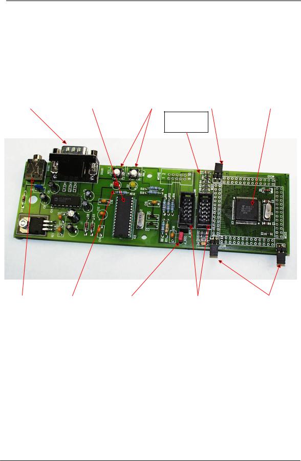
2.3.A Glance at the TOPAS900 Flash Board
After removing the plastic cover from the PCB you should see the following (for the picture below the cable connection between the Programming-and Debugging Board and the Flash Carrier Board has been removed to avoid covering components, this cable must be plugged in by default):
RS232-Connector |
|
Firmware-Processor |
|
RESET and NMI |
|
EA (external access) |
|
Flash MCU |
D-SUB 9 |
|
TMP87P808 |
|
Switches |
|
Jumper |
|
TMP95FY64F |
|
|
|
|
|
|
|
|
|
Scratch on PCB to break off
Power |
|
Status LED |
|
Jumper for Carrier |
|
Programming Board <=> |
|
Chip Select Jumpers |
Connector |
|
|
Board Vcc |
|
Carrier Board Connectors |
|
||
|
|
|
|
|
|
|||
|
|
|
|
|
|
|
|
|
Figure 1 : The TOPAS900 Flash Board (Top View)
As shown in the picture above the TOPAS900 Flash PCB can be divided into two functional groups: On the left side the “Programmingand DebuggingBoard” is located. On the right there is the “Flash Carrier Board”, surrounded by four 26-pin connectors (not soldered). The PCB is delivered in one piece.
The Flash Carrier Board can also be used independently from the Programming and Debugging Board. For independent usage it must be separated from the main board by breaking it off.
To break the Flash Carrier Board off please use this technique: Remove the connection cable between the two parts when plugged in. Put the TOPAS900 Flash board on a flat and stable surface. Keep the scratch between “Programming-and-Debugging Part” and
HWU Elektronik Oberhausen |
Page 8 |
Users Manual TOPAS900 Flash V2.1
“Flash Carrier Part” exactly onto the edge of the surface (see also fig. 2). Push down both parts carefully until the board breaks into two parts. By breaking into two parts the electrical circuitry is not modified in any way. It is just a mechanical separation.
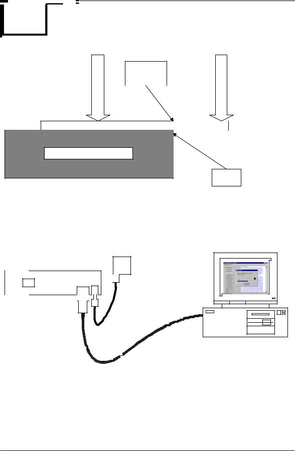
Scratch on the
PCB
Push |
|
Push |
|
TOPAS900 Flash Board |
Flash Carrier |
Desk or other stable basis |
|
|
Edge |
Figure 2 : Breaking off TOPAS900 Flash Board from Flash Carrier Board
2.4.Principe of Connection
The components are to be connected as the scheme below demonstrates:
|
|
AC Power Net |
Net |
|
|
|
|
|
Plug |
|
|
Flash
Carrier
Programming & Debugging
Board
Board
Null-Modem Cable
RS232 with 38400 baud
Windows-based PC
Figure 3 : Principe of Connection
HWU Elektronik Oberhausen |
Page 9 |

Users Manual TOPAS900 Flash V2.1
3.Hardware Description
TOPAS900 Flash consists of two boards: Programming-and-Debugging Board and Flash Carrier Board.
3.1.Programming and Debugging Board
As the name betrays this board is for programming and debugging purposes. The firmware processor, a TMP87P808P, is listening the serial data communication between a PC and the TOPAS900 Flash board. The firmware reacts on special data sequences to switch the target processor to several modes.
The Programming and Debugging is composed of the following components (to understand the design in detail it is recommended to make a print out of the schematics shown at the end of this manual):
∙Firmware Processor
∙Power supply
∙Status LEDs
∙Control Switches (Reset and NMI)
∙Serial Communication, Connector and Line Driver
∙Connector to Flash Carrier Board
3.1.1. Firmware Processor
A Toshiba TMP87P808 8-bit microcontroller of the TLCS-870 family is used. It is driven by an 8 MHz quartz resonator.
The processor drives control lines of the target system (Flash Carrier Board with TMP95FY64). The lines are /EA, /BOOT and /RESET. With these lines the target processor can de driven into several modes that are selected by the rising edge of the RESET input. Please refer to the manual for further information on Single Boot Mode / Single Chip Mode and Multi Chip Mode. Also read the information given by the memory maps later in this manual.
To control the target system the firmware is listening to the serial communication for certain binary control sequences that are generated by the Windows-based Flash Programming Tool. If a control sequence match is detected, the firmware processor switches the target system into the required mode.
3.1.2. Power Supply
The power supply is mainly build by the net plug and a 5V voltage regulator. Because the board has no on/off switch unplug the power plug from the board when connecting or disconnecting the target or when connecting the Flash Carrier Board to another application. The input power (at the board’s power plug) can be up to 12 V DC.
HWU Elektronik Oberhausen |
Page 10 |
Users Manual TOPAS900 Flash V2.1
3.1.3. Status LEDs
There are two status LEDs on the board. A red one and a yellow one. The red Led is controlled by the firmware processor and the yellow led is driven by the Flash MCU on the Flash Carrier Board. The yellow Led can be used as a very simple output device to show a internal state. Take a look at the LedDim sample to see how a Led can be dimmed by pulse-width modulation.
3.1.4. Control Switches (Reset and NMI)
On the Programming and Debugging Board two switches (keys) are mounted. The Resetswitch resets the firmware processor. After reset it lets boot the Flash MCU from external flash memory. Normally the external memory contains one of the two ROM monitors (IAR/Toshiba).
The second switch is to give a falling edge to the Flash MCU's NMI (non-maskable interrupt) input. The Toshiba ROM monitor reacts with stopping the user software, if it runs.
3.1.5. Serial Communication, Connector and Line Driver
The serial communication is build by a null-modem cable connected between the PC and the TOPAS900 Flash Board. For connection the board has a 9-pin D-sub male connector. To adapt the level between RS-232 and TTL a common RS-232 line driver is used. The serial communication between PC and firmware controller uses the parameter 9600,8,N,1. This baudrate is only used for control commands. The communication speed between Windows-Software and MCU on the Flash Carrier Board is always 38400 baud.
The communication uses the TxD and RxD lines only. These two lines are directly wired with the 10-pin connector to the Flash MCU. The firmware controller is connected in parallel. Both, the firmware processor and the Flash MCU are connected to the RxD and TxD line. To avoid both processors sending data to the same line the firmware processor switches it TxD output to high impedance when it is not used by the firmware itself.
3.1.6. Connector to Flash Carrier Board
To connect the Flash Carrier Board a 10-pin connector is mounted at the edge of the board. The 10-pin cable is to be plugged in on both sides to connect both boards together.
3.2.The Flash Carrier Board
The Flash Carrier Board is composed of the following parts:
∙The TMP95FY64F Microcontroller
∙512 kb Flash ROM TC58F400 (90 ns)
∙128 kb RAM TC551001 (70 ns)
∙Connector to Programming and Debugging Board
∙MCU Terminal Connectors
∙Jumpers
HWU Elektronik Oberhausen |
Page 11 |

Users Manual TOPAS900 Flash V2.1
3.2.1. The TMP95FY64F Microcontroller
The Flash Carrier Board has the main component of the starter kit soldered on it: the Toshiba TMP95FY64F microcontroller.
To get an overview of its powerful features lets have a look to its original data sheet (extract):
...
1.TMP95FY64F Basic Specification
1.1Outline and Feature
TMP95FY64 is high-speed advanced 16-bit microcontroller developed for controlling medium to largescale equipment. TMP95FY64 has 256K-Byte Flash memory which can be rewritten and erased on board. TMP95FY64 is housed in QFP-100pin package.
Device characteristics are as follows:
(1) Original High speed 16-bit CPU(900/H CPU)
TLCS-90/900 instruction mnemonic upward compatible. 16M-byte linear address space
General-purpose registers and register bank system
16-bit multiplication/ division and bit transfer/arithmetic instructions Micro DMA :4 channels(640ns/2bytes at 25MHz)
(2)Minimum instruction execution time:160ns at 25MHz
(3)Internal RAM:8Kbyte
Internal ROM:256Kbyte Flash memory
(4) External memory expansion
Can be expanded up to 16M byte (for both programs and data) AM8/16pin (select the external data bus width)
Can mix 8- and 16-bit external data buses. ....... Dynamic data bus sizing
(5) 8-bit timer:8 channels
Including event counter function(2 channels)
(6)16-bit timer/event counter:2 channels
(7)Serial interface:3 channels
(8)10-bit A/D converter:8 channels
(9)8-bit D/A converter:2 channels
(10)Watchdog timer
(11)Chip select/wait controller:4 blocks
(12)Interrupt functions:45-Interrupt sources
9-CPU interrupts ..... |
SWI instruction, and Illegal instruction |
|
26-Internal interrupts |
..... |
7-level priority can be set. |
10-External interrupts ..... |
7-level priority can be set. |
|
(13) I/O ports : Single chip mode 81 pins
Multi chip mode 55 pins(at AM8/16="H")
(14)Standby function:4 HALT mode(RUN,IDLE2,IDLE1,STOP)
(15)Operating Voltage : Vcc = 4.5 to 5.5V
(16)Package:100pin QFP(LFFP100-P-1414-0.50C:Thickness 2.4mm)
...
To get an overview on the internal organization of the TMP95FY64 let’s have a look to its schematic block diagram:
HWU Elektronik Oberhausen |
Page 12 |

Users Manual TOPAS900 Flash V2.1
Figure 4 : TMP95FY64 Schematic Block Diagram
3.2.2. 512 kb Flash ROM - Toshiba TC58F400 (90 ns)
This memory component is soldered on the bottom side of the PCB. It has a size of 512 kb. The chip can contain any software and data that fit into 512 kb. On delivery it contains the IAR ROM monitor.
The device can be addressed in 8 bit (byte) or 16 bit (word) organization. In case of the present starter kit it is wired by an 8-bit data bus. The disadvantage of lower operating speed is equalized by the gain of 8 port pins that are free for application purposes.
The external flash ROM is addressed by 19 address lines A0..18. The data lines are D0..D7 and the chip is selected by /CS2 pin of the MCU. The type of operation is selected by the /WR and /RD line accordingly. The /BYTE input is fixed to low level so that the byte mode is activated.
HWU Elektronik Oberhausen |
Page 13 |

Users Manual TOPAS900 Flash V2.1
Please refer to the memory maps to get information about the address range of the chip in memory.
3.2.3. 128 kb RAM - Toshiba TC551001 (70 ns)
This memory component is soldered on the bottom side of the PCB. It has a size of 128 kb and is organized in 8-bit words. It is addressed by 17 address lines A0..16. The data lines are D0..D7 and the chip is selected by /CS0 pin of the MCU. The type of operation is selected by the /WR and /RD line accordingly.
Please refer to the memory maps to get information about the address range of the chip in memory. The external RAM is used additionally to the internal RAM of 8 kb of the MCU. When the Toshiba ROM monitor is running almost 32 kb are allocated to the ROM monitor. For all monitor operations the RAM is mapped to address 0xFE0000..0xFFFFFF and covers the interrupt vector area that must be writable for debugging purposes.
3.2.4. Connector to Programming and Debugging Board
To connect the Programming and Debugging Board a 10-pin connector is mounted at the edge of the board. The 10-pin cable is to be plugged in on both sides to connect both boards together.
3.2.5. MCU Terminal Connectors
The Flash Carrier Board can be used - when properly programmed - stand-alone in a user’s application. For this kind of usage it is necessary to insert and solder four 26-pin connectors into the prepared drill holes. The prepared space for the connectors can easily found by searching the Flash Carrier Board for the printed labels “MCU1”, “MCU2”, “MCU3” and “MCU4”. The connections to the MCU are made as easy as possible. Each of the 100 pins of the MCU are connected directly to MCU connectors. E.g. pin 11 of the MCU is wired with pin11 of “MCU1” connector. Pin 26 of each connector is left out and not connected (the MCU has 100 pins, but 4x26=104). It is recommended to do direct measurement at the terminal connectors (or their metalized drill holes) instead of contacting the very small and sensitive MCU pins.
3.2.6. Jumpers
J_CS0 : This jumper is to connect/disconnect the chip select line CS0 to the on-board RAM device. If an external data/address bus is not required, it is recommended to open this jumper. The CS0 pin can be used as a port pin additionally.
J_CS2 : Same as above. The CS2 pin is used to enable the on-board flash ROM device.
J_EA : Jumper to select between internal (high/open) and external flash memory access (low/closed) after reset. When the Flash Carrier Board is connected to the Programming
HWU Elektronik Oberhausen |
Page 14 |
 Loading...