

Texas Instruments CD74HCT4053PWR, CD74HCT4053M96, CD74HCT4053M, CD74HCT4053E, CD74HCT4052M96 Datasheet
...
Data sheet acquired from Harris Semiconductor
SCHS122A
November 1997 - Revised April 1999
CD54HC4051,
CD74HC4051, CD74HCT4051,
CD74HC4052, CD74HCT4052,
CD74HC4053, CD74HCT4053
High Speed CMOS Logic
Analog Multiplexers/Demultiplexers
[ /Title
(CD54
HC405
1,
CD74
HC405
1,
CD74
HCT40
51,
CD74
HC405
2,
Features
• Wide Analog Input Voltage Range . . . . . . . . . . ±5V Max
• Low “On” Resistance
-70Ω Typical (V
-40Ω Typical (V
• Low Crosstalk between Switches
• Fast Switching and Propagation Speeds
• “Break-Before-Make” Switching
• Wide Operating Temperature Range . . -55
• CD54HC/CD74HC Types
- Operation Control Voltage . . . . . . . . . . . . . . 2V to 6V
- Switch Voltage . . . . . . . . . . . . . . . . . . . . . . .0V to 10V
- High Noise Immunity . . . N
V
= 5V
CC
• CD54HCT/CD74HCT Types
- Operation Control Voltage . . . . . . . . . . . 4.5V to 5.5V
- Switch Voltage . . . . . . . . . . . . . . . . . . . . . . . 0V to 10V
- Direct LSTTL Input
Logic Compatibility . . . V
- CMOS Input Compatibility. . . . . I
- VEE = 4.5V)
CC
- VEE = 9V)
CC
o
C to 125oC
= 30%, NIH = 30% of VCC,
IL
= 0.8V Max, VIH = 2V Min
IL
≤ 1µA at VOL, V
I
OH
Description
These devices are digitally controlled analog switches which
utilize silicon gate CMOS technology to achieve operating
speeds similar to LSTTL with the low power consumption of
standard CMOS integrated circuits.
These analog multiplexers/demultiplexers control analog
voltages that may vary across the voltage supply range (i.e.
V
to VEE). They are bidirectional switches thus allowing
CC
any analog input to be used as an output and visa-versa.
The switches have low “on” resistance and low “off” leakages. In addition, all three devices have an enable control
which, when high, disables all switches to their “off” state.
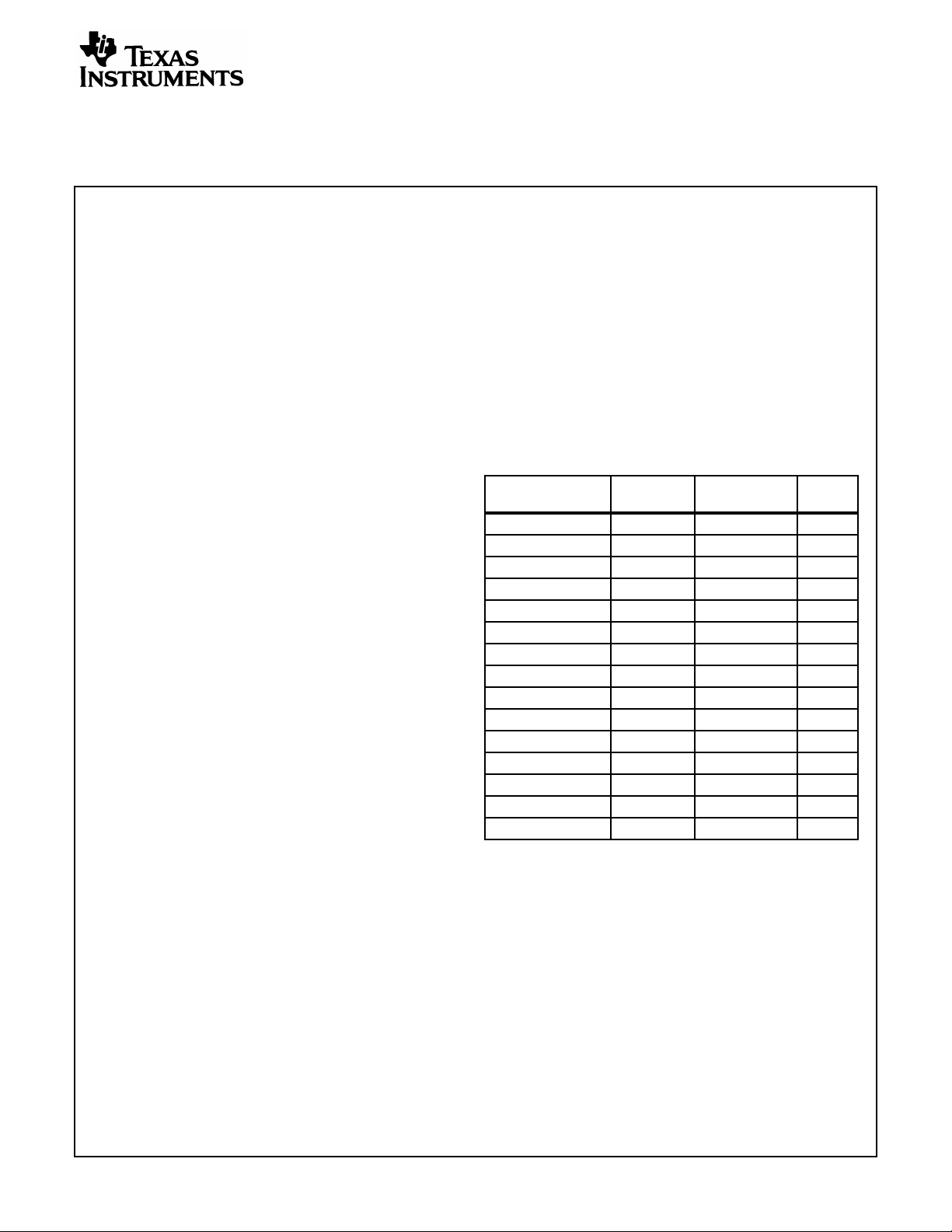
Ordering Information
TEMP.
PART NUMBER
CD54HC4051F -55 to 125 16 Ld CERDIP F16.3
CD74HC4051E -55 to 125 16 Ld PDIP E16.3
CD74HC4052E -55 to 125 16 Ld PDIP E16.3
CD74HC4053E -55 to 125 16 Ld PDIP E16.3
CD74HCT4051E -55 to 125 16 Ld PDIP E16.3
CD74HCT4052E -55 to 125 16 Ld PDIP E16.3
CD74HCT4053E -55 to 125 16 Ld PDIP E16.3
CD74HC4051M -55 to 125 16 Ld SOIC M16.15
CD74HC4052M -55 to 125 16 Ld SOIC M16.15
CD74HC4053M -55 to 125 16 Ld SOIC M16.15
CD74HCT4051M -55 to 125 16 Ld SOIC M16.15
CD74HCT4052M -55 to 125 16 Ld SOIC M16.15
CD74HCT4053M -55 to 125 16 Ld SOIC M16.15
CD74HCT4053PW -55 to 125 16 Ld TSSOP
CD74HCT4052SM -55 to 125 16 Ld SSOP M16.15A
NOTES:
1. When ordering, usethe entire part number. Add thesuffix 96to
obtain the variant in the tape and reel. For the TSSOP package
only, add the suffix R to obtain the variant in the tape and reel.
2. Waferor die is available which meets all electrical specifications.
Please contact your local salesoffice or Harris customerservice
for ordering information.
RANGE (oC) PACKAGE
PKG.
NO.
CAUTION: These devices are sensitive to electrostatic discharge. Users should follow proper IC Handling Procedures.
Copyright
© Harris Corporation 1997
1
File Number 1676.1
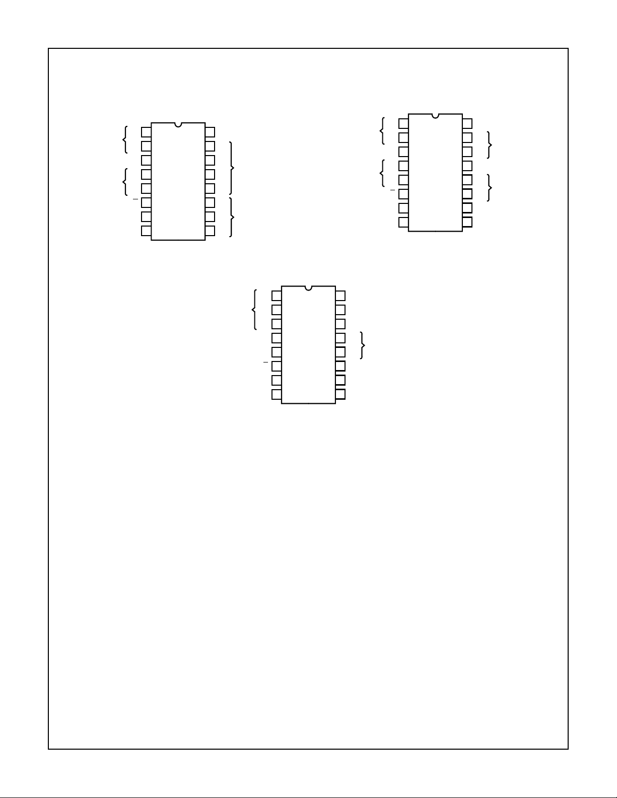
Pinouts
CD54HC4051, CD74HC4051, 52, 53; CD74HCT4051, 52, 53
CHANNEL
IN/OUT
COM OUT/IN
CHANNEL
IN/OUT
CD54HC4051
CD74HC4051, CD74HCT4051
(CERDIP, PDIP, SOIC)
TOP VIEW
16
A4
A6
A7
A5
V
EE
GND
1
2
A
3
4
5
6
E
7
8
V
A2
15
14
A1
13
A0
12
A3
S0
11
10
S1
S2
9
CHANNEL
COM OUT/IN
CC
IN/OUT
IN/OUT
CHANNEL
IN/OUT
ADDRESS
SELECT
CD74HC4053, CD74HCT4053
(PDIP, SOIC, TSSOP)
TOP VIEW
1
B1
2
B0
C1
3
C
4
N
5
C0
6
E
7
V
EE
8
GND
CHANNEL
IN/OUT
COM OUT/IN
CHANNEL
IN/OUT
16
V
CC
15
B
N
14
A
N
13
A1
12
A0
S0
11
10
S1
S2
9
CD74HC4052, CD74HCT4052
(PDIP, SOIC)
TOP VIEW
1
B0
2
B2
B
3
N
4
B3
5
B1
6
E
7
V
EE
8
GND
COM OUT/IN
COM OUT/IN
CHANNEL
IN/OUT
16
V
CC
A2
15
14
13
12
11
10
9
A1
A
A0
A3
S0
S1
N
CHANNEL
IN/OUT
COM OUT/IN
CHANNEL
IN/OUT
2
CD54HC4051, CD74HC4051, 52, 53; CD74HCT4051, 52, 53CD54HC4051, CD74HC4051, 52, 53; CD74HCT4051, 52, 53
Functional Diagram of HC/HCT4051
CHANNEL IN/OUT
V
CC
16
S
11
0
10
S
1
LOGIC
LEVEL
CONVERSION
S
9
2
6E
BINARY
TO
1 OF 8
DECODER
WITH
ENABLE
A
7A6A5A4A3A2A1A0
131415121524
TG
TG
TG
TG
TG
TG
TG
TG
3
A
COMMON
OUT/IN
8 7
GND V
X = Don’t care
EE
TRUTH TABLE
CD54/74HC/HCT4051
INPUT STATES
“ON”
2
S
1
S
0
CHANNELSENABLE S
L LLL A0
LLLH A1
LLHL A2
LLHH A3
LHLL A4
LHLH A5
LHHL A6
L HHH A7
H X X X None
3
CD54HC4051, CD74HC4051, 52, 53; CD74HCT4051, 52, 53CD54HC4051, CD74HC4051, 52, 53; CD74HCT4051, 52, 53
Functional Diagram of HC/HCT4052
V
CC
16
A CHANNELS IN/OUT
A
3A2A1A0
12141511
TG
TG
TG
BINARY
9
S
1
10
S
0
6E
LOGIC
LEVEL
CONVERSION
8 7
GND V
EE
TO
1 OF 4
DECODER
WITH
ENABLE
TRUTH TABLE
CD74HC4052, CD74HCT4052
INPUT STATES
1
S
0
L L L A0, B0
13
3
COMMON A
OUT/IN
COMMON B
OUT/IN
4251
B
0B1B2B3
B CHANNELS IN/OUT
TG
TG
TG
TG
TG
“ON”
CHANNELSENABLE S
L L H A1, B1
L H L A2. B2
L H H A3, B3
H X X None
X = Don’t care
4
CD54HC4051, CD74HC4051, 52, 53; CD74HCT4051, 52, 53CD54HC4051, CD74HC4051, 52, 53; CD74HCT4051, 52, 53
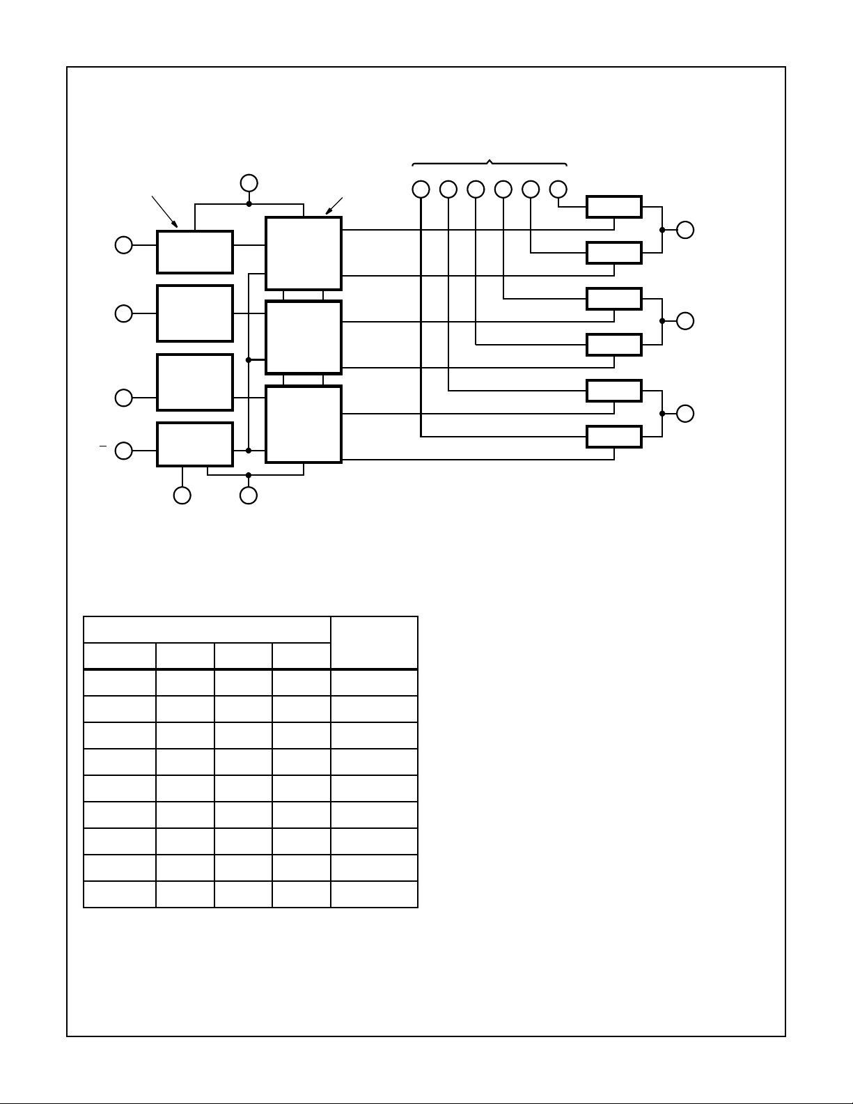
Functional Diagram of HC/HCT4053
LOGIC LEVEL
CONVERSION
11
S
0
10
S
1
S
9
2
6E
8
GND V
V
CC
16
7
EE
BINARY TO
1 OF 2
DECODERS
WITH ENABLE
C1C0B1B0A1A
IN/OUT
0
12132153
TG
A COMMON
14
OUT/IN
TG
TG
B COMMON
15
OUT/IN
TG
TG
C COMMON
4
OUT/IN
TG
TRUTH TABLE
CD74HC4053, CD74HCT4053
INPUT STATES
0
S
1
S
2
L L L L C0, B0, A0
L H L L C0, B0, A1
L L H L C0, B1, A0
L H H L C0, B1, A1
L L L H C1, B0, A0
L H L H C1, B0, A1
L L H H C1, B1, A0
L H H H C1, B1, A1
H X X X None
X = Don’t care
“ON”
CHANNELSENABLE S
5
CD54HC4051, CD74HC4051, 52, 53; CD74HCT4051, 52, 53CD54HC4051, CD74HC4051, 52, 53; CD74HCT4051, 52, 53
Absolute Maximum Ratings (Note 3) Thermal Information
DC Supply Voltage, VCC - VEE . . . . . . . . . . . . . . . . . -0.5V to 10.5V
DC Supply Voltage, V
DC Supply Voltage, V
DC Input Diode Current, I
CC. . . . . . . . . . . . . . . . . . . . . . . . . . . . -0.5V to +7V
EE . . . . . . . . . . . . . . . . . . . . . . . . . . . . +0.5V to -7V
IK
For VI < -0.5V or VI > VCC + 0.5V. . . . . . . . . . . . . . . . . . . . . .±20mA
DC Switch Diode Current, I
OK
For VI < VEE -0.5V or VI > VCC + 0.5V . . . . . . . . . . . . . . . . .±20mA
DC Switch Current, (Note 2)
For VI > VEE -0.5V or VI < VCC + 0.5V . . . . . . . . . . . . . . . . .±25mA
DC VCC or Ground Current, ICC . . . . . . . . . . . . . . . . . . . . . . . . .±50mA
DC VEE Current, IEE . . . . . . . . . . . . . . . . . . . . . . . . . . . . . . . -20mA
Recommended Operating Conditions For maximum reliability, nominal operating conditions should be selected so that
operation is always within the following ranges
PARAMETER MIN MAX UNITS
Supply Voltage Range (For T
CD54/74HC Types 26V
CD54/74HCT Types 4.5 5.5 V
Supply Voltage Range (For TA = Full Package Temperature Range), VCC - V
CD54/74HC Types, CD54/74HCT Types (See Figure 1) 2 10 V
Supply Voltage Range (For TA = Full Package Temperature Range), VEE (Note 5)
CD54/74HC Types, CD54/74HCT Types (See Figure 2) 0 -6 V
DC Input Control Voltage, V
Analog Switch I/O Voltage, V
Operating Temperature, T
Input Rise and Fall Times, tr, t
2V 0 1000 ns
4.5V 0 500 ns
6V 0 400 ns
CAUTION: Stresses above those listed in “Absolute Maximum Ratings” may cause permanent damage to the device. This is a stress only rating and operation
of the device at these or any other conditions above those indicated in the operational sections of this specification is not implied.
NOTES:
3. All voltages referenced to GND unless otherwise specified.
4. θJA is measured with the component mounted on an evaluation PC board in free air.
5. Incertain applications, the external load resistor current may include both VCCandsignal line components. To avoid drawing VCCcurrent
when switch current flows into the transmission gate inputs, the voltage drop across the bidirectional switch must not exceed 0.6V (calculated from rONvalues shown in Electrical Specifications table). No VCCcurrent will flow through RLif the switch current flows into
terminal 3 on the HC/HCT4051; terminals 3 and 13 on the HC/HCT4052; terminals 4, 14 and 15 on the HC/HCT4053.
= Full Package Temperature Range), VCC (Note 5)
A
I
IS
A
f
Thermal Resistance (Typical, Note 4) θJA (oC/W) θJC (oC/W)
PDIP Package. . . . . . . . . . . . . . . . . . . 90 N/A
SOIC Package. . . . . . . . . . . . . . . . . . . 160 N/A
CERDIP Package . . . . . . . . . . . . . . . . 130 55
TSSOP Package . . . . . . . . . . . . . . . . . 149 35
Maximum Junction Temperature. . . . . . . . . . . . . . . . . . . . . . . 150oC
Maximum Storage Temperature Range . . . . . . . . . .-65oC to 150oC
Maximum Lead Temperature (Soldering 10s). . . . . . . . . . . . . 300oC
EE
GND V
V
EE
V
-55 125
CC
CC
V
V
o
C
Recommended Operating Area as a Function of Supply Voltages
8
6
HC
4
- GND (V)
CC
2
V
0
024681012
VCC - VEE (V)
FIGURE 1. FIGURE 2.
HCT
6
8
6
4
- GND (V)
CC
2
V
0
0-2-4-6-8
HCT
VEE - GND (V)
HC

CD54HC4051, CD74HC4051, 52, 53; CD74HCT4051, 52, 53CD54HC4051, CD74HC4051, 52, 53; CD74HCT4051, 52, 53
DC Electrical Specifications
TEST CONDITIONS AMBIENT TEMPERATURE, T
25oC -40oC - 85oC -55oC - 125oC
MIN TYP MAX MIN MAX MIN MAX
PARAMETER
V
(V)
V
V
IS
I
(V)
(V)
EE
V
CC
(V)
HC TYPES
High Level Input Voltage,
V
IH
2 1.5 - - 1.5 - 1.5 - V
4.5 3.15 - - 3.15 - 3.15 0 V
6 4.2 - - 4.2 - 4.2 - V
Low Level Input Voltage,
V
IL
2 - - 0.5 - 0.5 - 0.5 V
4.5 - - 1.35 - 1.35 - 1.35 V
6 - - 1.8 - 1.8 - 1.8 V
On Resistance, r
ON
IO = 1mA, (Figure 11)
VCC or V
EE
VIL or
V
IH
0 4.5 - 70 160 - 200 - 240 Ω
0 6 - 60 140 - 175 - 210 Ω
-4.5 4.5 - 40 120 - 150 - 180 Ω
VCC to V
EE
0 4.5 - 90 180 - 225 - 270 Ω
0 6 - 80 160 - 200 - 240 Ω
-4.5 4.5 - 45 130 - 162 - 195 Ω
Maximum On Resistance
Between any Two
Channels, ∆r
ON
04.5-10-----Ω
06-8.5-----Ω
-4.5 4.5 - 5 - ----Ω
Switch On/Off Leakage
Current, I
IZ
1 and 2 Channels 0 6 - - ±0.1 - ±1-±1µA
4053 -5 5 - - ±0.1 - ±1-±1µA
For Switch Off:
When VIS=VCC,
VOS = VEE;
When VIS=VEE,
VOS = V
CC
VIL or
V
IH
For Switch On:
4 Channels 0 6 - - ±0.1 - ±1-±1µA
4052 -5 5 - - ±0.2 - ±2-±2µA
8 Channels 0 6 - - ±0.2 - ±2-±2µA
All Applicable
Combinations of
VIS and V
OS
Voltage Levels
4051 -5 5 - - ±0.4 - ±4-±4µA
Control Input Leakage
Current, I
IL
Quiescent Device
Current, I
CC
IO = 0
When VIS=VEE,
VOS = V
CC
When VIS=VCC,
VOS = V
EE
VCC or
GND
VCC or
GND
06 - -±0.1 - ±1-±1µA
0 6 - - 8 - 80 - 160 µA
-5 5 - - 16 - 160 - 320 µA
A
UNITS
7

CD54HC4051, CD74HC4051, 52, 53; CD74HCT4051, 52, 53CD54HC4051, CD74HC4051, 52, 53; CD74HCT4051, 52, 53
DC Electrical Specifications (Continued)
TEST CONDITIONS AMBIENT TEMPERATURE, T
25oC -40oC - 85oC -55oC - 125oC
MIN TYP MAX MIN MAX MIN MAX
PARAMETER
V
(V)
V
V
IS
I
(V)
(V)
EE
V
CC
(V)
HCT TYPES
High Level Input Voltage,
V
IH
Low Level Input Voltage,
V
IL
On Resistance, r
ON
IO = 1mA, (Figure 15)
VCC or V
EE
VIL or
V
IH
4.5to
2--2-2-V
5.5
4.5to
- - 0.8 - 0.8 - 0.8 V
5.5
0 4.5 - 70 160 - 200 - 240 Ω
---------Ω
-4.5 4.5 - 40 120 - 150 - 180 Ω
VCC to V
EE
0 4.5 - 90 180 - 225 - 270 Ω
---------Ω
-4.5 4.5 - 45 130 - 162 - 195 Ω
Maximum On Resistance
Between any Two
Channels, ∆r
ON
04.5-10-----Ω
---------Ω
-4.5 4.5 - 5 - ----Ω
Switch On/Off Leakage
Current, I
IZ
1 and 2 Channels 0 6 - - ±0.1 - ±1-±1µA
4053 -5 5 - - ±0.1 - ±1-±1µA
For Switch Off:
When VIS=VCC,
VOS = VEE;
When VIS=VEE,
VOS = V
CC
VIL or
V
IH
For Switch On:
4 Channels 0 6 - - ±0.1 - ±1-±1µA
4052 -5 5 - - ±0.2 - ±2-±2µA
8 Channels 0 6 - - ±0.2 - ±2-±2µA
All Applicable
Combinations of
VIS and V
OS
Voltage Levels
4051 -5 5 - - ±0.4 - ±4-±4µA
Control Input Leakage
Current, I
IL
Quiescent Device
Current, I
CC
IO = 0
Additional Quiescent
Device Current, ∆I
CC
- (Note 7) - 5.5 - - ±0.1 - ±1-±1µA
When VIS=VEE,
VOS = V
CC
When VIS=VCC,
VOS = V
EE
VCC or
GND
VCC -
2.1
0 5.5 - - 8 - 80 - 160 µA
-4.5 5.5 - - 16 - 160 - 320 µA
4.5to
- 100 360 - 450 - 490 µA
5.5
(Note 6)
Per Input Pin: 1 Unit
Load
NOTES:
6. For dual supply systems theoretical worst case (VI = 2.4V, VCC = 5.5V) specification is 1.8mA.
7. Any voltage between VCC and GND.
A
UNITS
HCT Input Loading Table
UNIT LOADS
TYPE INPUT
4051, 4053 All 0.5
4052 All 0.4
NOTE: Unit load is ∆ICC limit specified in DC Specifications table,
e.g., 360mA max. at 25oC.
(NOTE)
8

CD54HC4051, CD74HC4051, 52, 53; CD74HCT4051, 52, 53CD54HC4051, CD74HC4051, 52, 53; CD74HCT4051, 52, 53
Switching Specifications V
= 5V, TA = 25oC, Input tr, tr = 6ns
CC
TYPICAL
4051 4052 4053
C
L
PARAMETER
(pF)
HC HCT HC HCT HC HCT
UNITS
Propagation Delay
Switch IN to OUT, t
Switch Turn-Off (S or E), t
Switch Turn-On (S or E), t
PHL
, t
PLH
PHZ,tPLZ
PZH
15444444ns
15 19 19 21 21 18 18 ns
, t
PZL
15 19 23 27 29 18 20 ns
Power Dissipation Capacitance, CPD (Note 8) - 50 52 74 76 38 42 pF
NOTE:
8. CPD is used to determine the dynamic power consumption, per package.
PD = CPD V
2
fI + ∑ (CL + CS) V
CC
CC
2
f
O
fO = output frequency
fI = input frequency
CL = output load capacitance
CS = switch capacitance
VCC = supply voltage
Switching Specifications C
= 50pF, Input tr, tr = 6ns
L
AMBIENT TEMPERATURE, T
A
25oC -40oC - 85oC -55oC - 125oC
PARAMETER
Propagation Delay, Switch
In to Out, t
Maximum Switch
PLH
, t
PHL
4051 0 2 - 225 - - - 280 - - - 340 - - ns
Turn “Off” Delay
from S or E to
Switch Output
t
, t
PHZ
PLZ
4052 0 2 - 250 - - - 315 - - - 375 - - ns
4053 0 2 - 210 - - - 265 - - - 315 - - ns
V
V
EE
CC
(V)
(V)
MIN MAX MIN MAX MIN MAX MIN MAX MIN MAX MIN MAX
UNITS
02-60---75---90--ns
0 4.5 - 12 - 12 - 15 - 15 - 18 - 18 ns
06-10---13---15--ns
-4.5 4.5 - 8 - 8 - 10 - 10 - 12 - 12 ns
0 4.5 - 45 - 45 - 56 - 56 - 68 - 68 ns
06-38---48---57--ns
-4.5 4.5 - 32 - 32 - 40 - 40 - 48 - 48 ns
0 4.5 - 50 - 50 - 63 - 63 - 75 - 75 ns
06-43---54---65--ns
-4.5 4.5 - 38 - 38 - 48 - 48 - 57 - 57 ns
0 4.5 - 42 - 44 - 53 - 55 - 63 - 66 ns
HC HCT HC HCT HC HCT
06-36---45---54--ns
-4.5 4.5 - 29 - 31 - 36 - 39 - 44 - 47 ns
9

CD54HC4051, CD74HC4051, 52, 53; CD74HCT4051, 52, 53CD54HC4051, CD74HC4051, 52, 53; CD74HCT4051, 52, 53
Switching Specifications C
V
EE
PARAMETER
Maximum Switch
Turn “On” Delay
from S or E to
Switch Output
t
, t
PZL
PZH
(V)
4051 0 2 - 225 - - - 280 - - - 340 - - ns
0 4.5 - 45 - 55 - 56 - 69 - 68 - 83 ns
06-38---48---57--ns
-4.5 4.5 - 32 - 39 - 40 - 49 - 48 - 59 ns
4052 0 2 - 325 - - - 405 - - - 490 - - ns
0 4.5 - 65 - 70 - 81 - 68 - 98 - 105 ns
06-55---69---83--ns
-4.5 4.5 - 46 - 48 - 58 - 60 - 69 - 72 ns
4053 0 2 - 220 - - - 275 - - - 330 - - ns
0 4.5 - 44 - 48 - 55 - 60 - 66 - 72 ns
06-37---47---56--ns
= 50pF, Input tr, tr = 6ns (Continued)
L
AMBIENT TEMPERATURE, T
A
25oC -40oC - 85oC -55oC - 125oC
HC HCT HC HCT HC HCT
V
CC
(V)
MIN MAX MIN MAX MIN MAX MIN MAX MIN MAX MIN MAX
UNITS
-4.5 4.5 - 31 - 34 - 39 - 43 - 47 - 51 ns
Input (Control)
Capacitance, C
I
- - - 10 - 10 - 10 - 10 - 10 - 10 pF
Analog Channel Specifications Typical Values at T
PARAMETER TEST CONDITIONS
Switch Input Capacitance, C
Common Output Capacitance, C
Minimum Switch Frequency Response at -3dB, f
(Figures 12, 14, 16)
I
COM
MAX
See Figure 3, Notes 9, 10 4051
= 25oC
A
HC/HCT
TYPES
V
(V)
EE
V
(V)
CC
HC/
HCT UNITS
All - - 5 pF
4051 - - 25 pF
4052 - - 12 pF
4053 - - 8 pF
145 MHz
4052 165 MHz
-2.25 2.25
4053 200 MHz
4051
4052 185 MHz
-4.5 4.5
180 MHz
4053 200 MHz
10

CD54HC4051, CD74HC4051, 52, 53; CD74HCT4051, 52, 53CD54HC4051, CD74HC4051, 52, 53; CD74HCT4051, 52, 53
Analog Channel Specifications Typical Values at T
PARAMETER TEST CONDITIONS
Crosstalk Between any Two Switches (Note 12) See Figure 4,
Sinewave Distortion See Figure 5 All -2.25 2.25 0.035 %
E or S to Switch Feedthrough Noise See Figure 6
Switch “OFF” Signal Feedthrough (Figures 13, 15, 17) See Figure 7
NOTES:
9. Adjust input voltage to obtain 0dBm at VOS for fIN = 1MHz.
10. VIS is centered at (VCC - VEE)/2.
11. Adjust input for 0dBm.
12. Not applicable for HC/HCT4051.
= 25oC
A
Notes 10, 11
Notes 10, 11
Notes 10, 11
HC/HCT
TYPES
4051
4052 (TBE) dB
4053 (TBE) dB
4051
4052 (TBE) dB
4053 (TBE) dB
All -4.5 4.5 0.018 %
4051
4052 mV
4053 mV
4051
4052 mV
4053 mV
4051
4052 -65 dB
4053 -64 dB
4051
4052 -67 dB
4053 -66 dB
V
EE
(V)
-2.25 2.25
-4.5 4.5
-2.25 2.25 (TBE)
-4.5 4.5 (TBE)
-2.25 2.25
-4.5 4.5
V
(V)
CC
HC/
HCT UNITS
N/A dB
N/A dB
-73 dB
-75 dB
mV
mV
11

CD54HC4051, CD74HC4051, 52, 53; CD74HCT4051, 52, 53
Test Circuits and Waveforms
V
IS
CC
SWITCH
ON
R
VCC/2
VCC/2
R
V
OS2
C
V
R
INPUT
V
CC
f
R = 50Ω
0.1µF
= 1MHz SINEWAVE
IS
C = 10pF
V
10pF
OS
dB
METER
V
CC
R
SWITCH
OFF
/2
V
CC
V
IS
0.1µF
SWITCH
ON
50Ω
/2
V
CC
FIGURE 3. FREQUENCY RESPONSE TEST CIRCUIT FIGURE 4. CROSSTALK BETWEEN TWO SWITCHES TEST
CIRCUIT
C
METER
dB
V
OS1
E
V
CC
SWITCH
ALTERNATING
ON AND OFF
t
, tf≤ 6ns
r
= 1MHz
f
CONT
50% DUTY
CYCLE
VCC/2
600Ω
V
OS
V
50pF
SINE-
WAVE
10µF
V
IS
fIS = 1kHz TO 10kHz
V
CC
SWITCH
ON
V
= V
I
10kΩ
IH
50pF
V
IS
V
OS
DISTORTION
600Ω
VCC/2
METER
/2
V
CC
FIGURE 5. SINEWAVE DISTORTION TEST CIRCUIT FIGURE 6. CONTROL TO SWITCH FEEDTHROUGH NOISE
TEST CIRCUIT
fIS≥ 1MHz SINEWAVE
V
CC
= V
V
0.1µF
V
IS
SWITCH
OFF
C
R
VCC/2
VCC/2
R = 50Ω
C = 10pF
IL
R
V
OS
C
dB
METER
OS
SCOPE
V
P-P
FIGURE 7. SWITCH OFF SIGNAL FEEDTHROUGH
12

CD54HC4051, CD74HC4051, 52, 53; CD74HCT4051, 52, 53
Test Circuits and Waveforms
t
r
SWITCH INPUT
SWITCH OUTPUT
6ns 6ns
E OR Sn
OUTPUT LOW
TO OFF
OUTPUT HIGH
TO OFF
SWITCH ON
50%
t
PLZ
t
PHZ
90%
10%
10%
t
90%
(Continued)
= 6ns tf = 6ns
t
PLH
t
PHL
FIGURE 8A.
6ns 6ns
E OR Sn
OUTPUT LOW
TO OFF
OUTPUT HIGH
TO OFF
1.3
t
t
SWITCH ON
t
PZL
PZH
50%
50%
SWITCH ONSWITCH OFF
V
CC
GND
PLZ
PHZ
V
CC
90%
50%
10%
V
EE
90%
50%
10%
t
r
10%
90%
t
2.7
f
0.3
t
PZL
t
PZH
3V
GND
50%
50%
SWITCH ONSWITCH OFF
FIGURE 8B. HC TYPES FIGURE 8C. HCT TYPES
FIGURE 8. SWITCH PROPAGATION DELAY, TURN-ON, TURN-OFF TIMES
OUT
VCC FOR
t
AND t
PLZ
V
FOR
EE
t
AND t
PHZ
PZL
PZH
t
t
PHZ
PLZ
VEE FOR
AND t
V
FOR
CC
AND t
PZL
PZH
= 1kΩ
R
TG
IN
L
C
L
50pF
FIGURE 9. SWITCH ON/OFF PROPAGATION DELAY TEST
CIRCUIT
IN
TG
OUT
50pF
FIGURE 10. SWITCH IN TO SWITCH OUT PROPAGATION
DELAY TEST CIRCUIT
13

CD54HC4051, CD74HC4051, 52, 53; CD74HCT4051, 52, 53
Typical Performance Curves
120
100
80
60
40
ON RESISTANCE (Ω)
20
VCC - VEE = 4.5V
VCC - VEE = 6V
VCC - VEE = 9V
123456789
INPUT SIGNAL VOLTAGE (V)
FIGURE 11. TYPICAL ON RESISTANCE vs INPUT SIGNAL VOLTAGE
0
VCC = 4.5V
-2
-4
dB
-6
-8
-10
10K 100K 1M 10M 100M
GND = -4.5V
= -4.5V
V
EE
= 50Ω
R
L
PIN 12 TO 3
FREQUENCY (Hz)
VCC = 2.25V
GND = -2.25V
= -2.25V
V
EE
= 50Ω
R
L
PIN 12 TO 3
0
-20
-40
dB
-60
-80
-100
10K 100K
VCC = 2.25V
GND = -2.25V
= -2.25V
V
EE
= 50Ω
R
L
PIN 12 TO 3
1M
FREQUENCY (Hz)
VCC = 4.5V
GND = -4.5V
= -4.5V
V
EE
= 50Ω
R
L
PIN 12 TO 3
10M 100M
FIGURE 12. CHANNEL ON BANDWIDTH (HC/HCT4051) FIGURE 13. CHANNEL OFF FEEDTHROUGH (HC/HCT4051)
0
VCC = 4.5V
-2
-4
dB
-6
-8
-10
10K 100K 1M 10M 100M
FREQUENCY (Hz)
GND = -4.5V
= -4.5V
V
EE
= 50Ω
R
L
PIN 4 TO 3
VCC = 2.25V
GND = -2.25V
= -2.25V
V
EE
= 50Ω
R
L
PIN 4 TO 3
0
VCC = 2.25V
-20
-40
dB
-60
-80
-100
10K 100K 1M 10M 100M
FREQUENCY (Hz)
GND = -2.25V
= -2.25V
V
EE
= 50Ω
R
L
PIN 4 TO 3
VCC = 4.5V
GND = -4.5V
= -4.5V
V
EE
= 50Ω
R
L
PIN 4 TO 3
FIGURE 14. CHANNEL ON BANDWIDTH (HC/HCT4052) FIGURE 15. CHANNEL OFF FEEDTHROUGH (HC/HCT4052)
14

CD54HC4051, CD74HC4051, 52, 53; CD74HCT4051, 52, 53
Typical Performance Curves
0
-1
-2
dB
-3
-4
10K 100K 1M 10M 100M
FREQUENCY (Hz)
(Continued)
VCC = 4.5V
GND = -4.5V
= -4.5V
V
EE
= 50Ω
R
L
PIN 5 TO 4
VCC = 2.25V
GND = -2.25V
= -2.25V
V
EE
= 50Ω
R
L
PIN 5 TO 4
0
-20
-40
dB
-60
-80
-100
10K 100K 1M 10M 100M
VCC = 2.25V
GND = -2.25V
= -2.25V
V
EE
= 50Ω
R
L
PIN 5 TO 4
FREQUENCY (Hz)
VCC = 4.5V
GND = -4.5V
= -4.5V
V
EE
= 50Ω
R
L
PIN 5 TO 4
FIGURE 16. CHANNEL ON BANDWIDTH (HC/HCT4053) FIGURE 17. CHANNEL OFF FEEDTHROUGH (HC/HCT4053)
15

16

IMPORTANT NOTICE
T exas Instruments and its subsidiaries (TI) reserve the right to make changes to their products or to discontinue
any product or service without notice, and advise customers to obtain the latest version of relevant information
to verify, before placing orders, that information being relied on is current and complete. All products are sold
subject to the terms and conditions of sale supplied at the time of order acknowledgement, including those
pertaining to warranty, patent infringement, and limitation of liability.
TI warrants performance of its semiconductor products to the specifications applicable at the time of sale in
accordance with TI’s standard warranty. Testing and other quality control techniques are utilized to the extent
TI deems necessary to support this warranty . Specific testing of all parameters of each device is not necessarily
performed, except those mandated by government requirements.
CERT AIN APPLICATIONS USING SEMICONDUCTOR PRODUCTS MAY INVOLVE POTENTIAL RISKS OF
DEATH, PERSONAL INJURY, OR SEVERE PROPERTY OR ENVIRONMENTAL DAMAGE (“CRITICAL
APPLICATIONS”). TI SEMICONDUCTOR PRODUCTS ARE NOT DESIGNED, AUTHORIZED, OR
WARRANTED TO BE SUITABLE FOR USE IN LIFE-SUPPORT DEVICES OR SYSTEMS OR OTHER
CRITICAL APPLICA TIONS. INCLUSION OF TI PRODUCTS IN SUCH APPLICATIONS IS UNDERST OOD TO
BE FULLY AT THE CUSTOMER’S RISK.
In order to minimize risks associated with the customer’s applications, adequate design and operating
safeguards must be provided by the customer to minimize inherent or procedural hazards.
TI assumes no liability for applications assistance or customer product design. TI does not warrant or represent
that any license, either express or implied, is granted under any patent right, copyright, mask work right, or other
intellectual property right of TI covering or relating to any combination, machine, or process in which such
semiconductor products or services might be or are used. TI’s publication of information regarding any third
party’s products or services does not constitute TI’s approval, warranty or endorsement thereof.
Copyright 1999, Texas Instruments Incorporated
 Loading...