

TEXAS INSTRUMENTS CD54HC4051F3A, CD54HC4052F3A, CD54HC4053F3A, CD54HCT4051F3A, CD74HC4051E Technical data
...
Data sheet acquired from Harris Semiconductor
SCHS122G
November 1997 - Revised July 2003
CD54/74HC4051, CD54/74HCT4051,
CD54/74HC4052, CD74HCT4052,
CD54/74HC4053, CD74HCT4053
High-Speed CMOS Logic
Analog Multiplexers/Demultiplexers
[ /Title
(CD54
HC405
1,
CD74
HC405
1,
CD74
HCT40
51,
CD74
HC405
2,
Features
• Wide Analog Input Voltage Range . . . . . . . . . . ±5V Max
• Low “On” Resistance
-70Ω Typical (V
-40Ω Typical (V
• Low Crosstalk between Switches
• Fast Switching and Propagation Speeds
• “Break-Before-Make” Switching
• Wide Operating Temperature Range . . -55
• CD54HC/CD74HC Types
- Operation Control Voltage . . . . . . . . . . . . . . 2V to 6V
- Switch Voltage . . . . . . . . . . . . . . . . . . . . . . .0V to 10V
- High Noise Immunity . . . N
V
= 5V
CC
• CD54HCT/CD74HCT Types
- Operation Control Voltage . . . . . . . . . . . 4.5V to 5.5V
- Switch Voltage . . . . . . . . . . . . . . . . . . . . . . . 0V to 10V
- Direct LSTTL Input
Logic Compatibility . . . V
- CMOS Input Compatibility. . . . . I
- VEE = 4.5V)
CC
- VEE = 9V)
CC
o
C to 125oC
= 30%, NIH = 30% of VCC,
IL
= 0.8V Max, VIH = 2V Min
IL
≤ 1µA at VOL, V
I
OH
Description
These devices are digitally controlled analog switches which
utilize silicon gate CMOS technology to achieve operating
speeds similar to LSTTL with the low power consumption of
standard CMOS integrated circuits.
These analog multiplexers/demultiplexers control analog
voltages that may vary across the voltage supply range (i.e.
V
to VEE). They are bidirectional switches thus allowing
CC
any analog input to be used as an output and vice-versa.
The switches have low “on” resistance and low “off” leakages. In addition, all three devices have an enable control
which, when high, disables all switches to their “off” state.
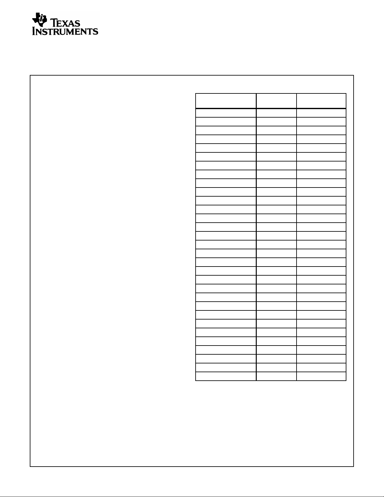
Ordering Information
TEMP. RANGE
PART NUMBER
CD54HC4051F3A -55 to 125 16 Ld CERDIP
CD54HC4052F3A -55 to 125 16 Ld CERDIP
CD54HC4053F3A -55 to 125 16 Ld CERDIP
CD54HCT4051F3A -55 to 125 16 Ld CERDIP
CD74HC4051E -55 to 125 16 Ld PDIP
CD74HC4051M -55 to 125 16 Ld SOIC
CD74HC4051M96 -55 to 125 16 Ld SOIC
CD74HC4051NSR -55 to 125 16 Ld SOP
CD74HC4051PWR -55 to 125 16 Ld TSSOP
CD74HC4052E -55 to 125 16 Ld PDIP
CD74HC4052M -55 to 125 16 Ld SOIC
CD74HC4052M96 -55 to 125 16 Ld SOIC
CD74HC4052NSR -55 to 125 16 Ld SOP
CD74HC4052PW -55 to 125 16 Ld TSSOP
CD74HC4052PWR -55 to 125 16 Ld TSSOP
CD74HC4053E -55 to 125 16 Ld PDIP
CD74HC4053M -55 to 125 16 Ld SOIC
CD74HC4053M96 -55 to 125 16 Ld SOIC
CD74HC4053NSR -55 to 125 16 Ld SOP
CD74HC4053PW -55 to 125 16 Ld TSSOP
CD74HC4053PWR -55 to 125 16 Ld TSSOP
CD74HCT4051E -55 to 125 16 Ld PDIP
CD74HCT4051M -55 to 125 16 Ld SOIC
CD74HCT4051M96 -55 to 125 16 Ld SOIC
CD74HCT4052E -55 to 125 16 Ld PDIP
CD74HCT4052M -55 to 125 16 Ld SOIC
CD74HCT4052M96 -55 to 125 16 Ld SOIC
CD74HCT4053E -55 to 125 16 Ld PDIP
CD74HCT4053M -55 to 125 16 Ld SOIC
CD74HCT4053M96 -55 to 125 16 Ld SOIC
CD74HCT4053PWR -55 to 125 16 Ld TSSOP
NOTE: When ordering, use the entire part number. The suffixes 96
and R denote tape and reel.
(oC) PACKAGE
CAUTION: These devices are sensitive to electrostatic discharge. Users should follow proper IC Handling Procedures.
Copyright
© 2003, Texas Instruments Incorporated
1
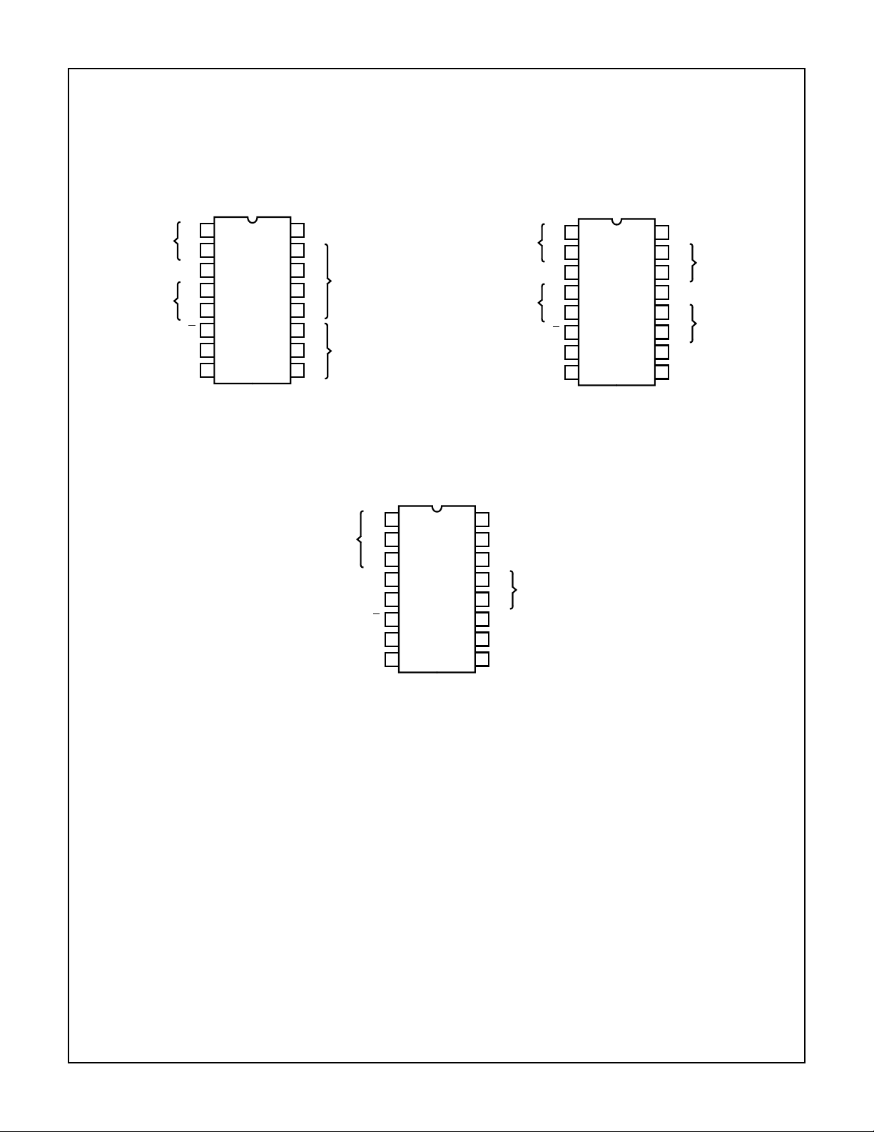
Pinouts
’HC4051, ’HCT4051, ’HC4052, CD74HCT4052, ’HC4053, CD74HCT4053
CHANNEL
IN/OUT
COM OUT/IN
CHANNEL
IN/OUT
CD54HC4051, CD54HCT4051
(CERDIP)
CD74HC4051
(PDIP, SOIC, SOP, TSSOP)
CD74HCT4051
(PDIP, SOIC)
TOP VIEW
16
A4
A6
A7
A5
V
EE
GND
1
2
3
A
4
5
6
E
7
8
V
15
A2
14
A1
A0
13
A3
12
S0
11
S1
10
9
S2
CHANNEL
COM OUT/IN
CC
IN/OUT
IN/OUT
CHANNEL
IN/OUT
ADDRESS
SELECT
CD54HC4053
(CERDIP)
CD74HC4053
(PDIP, SOIC, SOP, TSSOP)
CD74HCT4053
(PDIP, SOIC, TSSOP)
TOP VIEW
1
B1
2
B0
3
C1
4
C
N
5
C0
6
E
V
7
EE
8
GND
CHANNEL
IN/OUT
COM OUT/IN
CHANNEL
IN/OUT
16
V
CC
15
B
N
14
A
N
13
A1
12
A0
S0
11
10
S1
9
S2
CD54HC4052
(CERDIP)
CD74HC4052
(PDIP, SOIC, SOP, TSSOP)
CD74HCT4052
(PDIP, SOIC)
TOP VIEW
1
B0
2
B2
3
B
N
4
B3
5
B1
6
E
V
7
EE
8
GND
COM OUT/IN
COM OUT/IN
CHANNEL
IN/OUT
16
V
CC
15
A2
CHANNEL
9
A1
A
A0
A3
S0
S1
N
IN/OUT
COM OUT/IN
CHANNEL
IN/OUT
14
13
12
11
10
2
’HC4051, ’HCT4051, ’HC4052, CD74HCT4052, ’HC4053, CD74HCT4053’HC4051, ’HCT4051, ’HC4052, CD74HCT4052, ’HC4053, CD74HCT4053
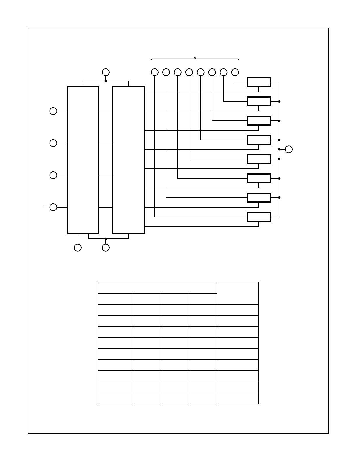
Functional Diagram of HC/HCT4051
CHANNEL IN/OUT
V
CC
16
S
11
0
10
S
1
LOGIC
LEVEL
CONVERSION
S
9
2
6E
BINARY
TO
1 OF 8
DECODER
WITH
ENABLE
A
7A6A5A4A3A2A1A0
131415121524
TG
TG
TG
TG
TG
TG
TG
TG
3
A
COMMON
OUT/IN
8 7
GND V
X = Don’t care
EE
TRUTH TABLE
HC/HCT4051
INPUT STATES
“ON”
2
S
1
S
0
CHANNELSENABLE S
L LLL A0
LLLH A1
LLHL A2
LLHH A3
LHLL A4
LHLH A5
LHHL A6
L HHH A7
H X X X None
3
’HC4051, ’HCT4051, ’HC4052, CD74HCT4052, ’HC4053, CD74HCT4053’HC4051, ’HCT4051, ’HC4052, CD74HCT4052, ’HC4053, CD74HCT4053
Functional Diagram of ’HC4052, CD74HCT4052
V
CC
16
A CHANNELS IN/OUT
A
3A2A1A0
12141511
TG
TG
TG
BINARY
9
S
1
10
S
0
6E
LOGIC
LEVEL
CONVERSION
8 7
GND V
EE
TO
1 OF 4
DECODER
WITH
ENABLE
TRUTH TABLE
’HC4052, CD74HCT4052
INPUT STATES
1
S
0
L L L A0, B0
13
3
COMMON A
OUT/IN
COMMON B
OUT/IN
4251
B
0B1B2B3
B CHANNELS IN/OUT
TG
TG
TG
TG
TG
“ON”
CHANNELSENABLE S
L L H A1, B1
L H L A2. B2
L H H A3, B3
H X X None
X = Don’t care
4
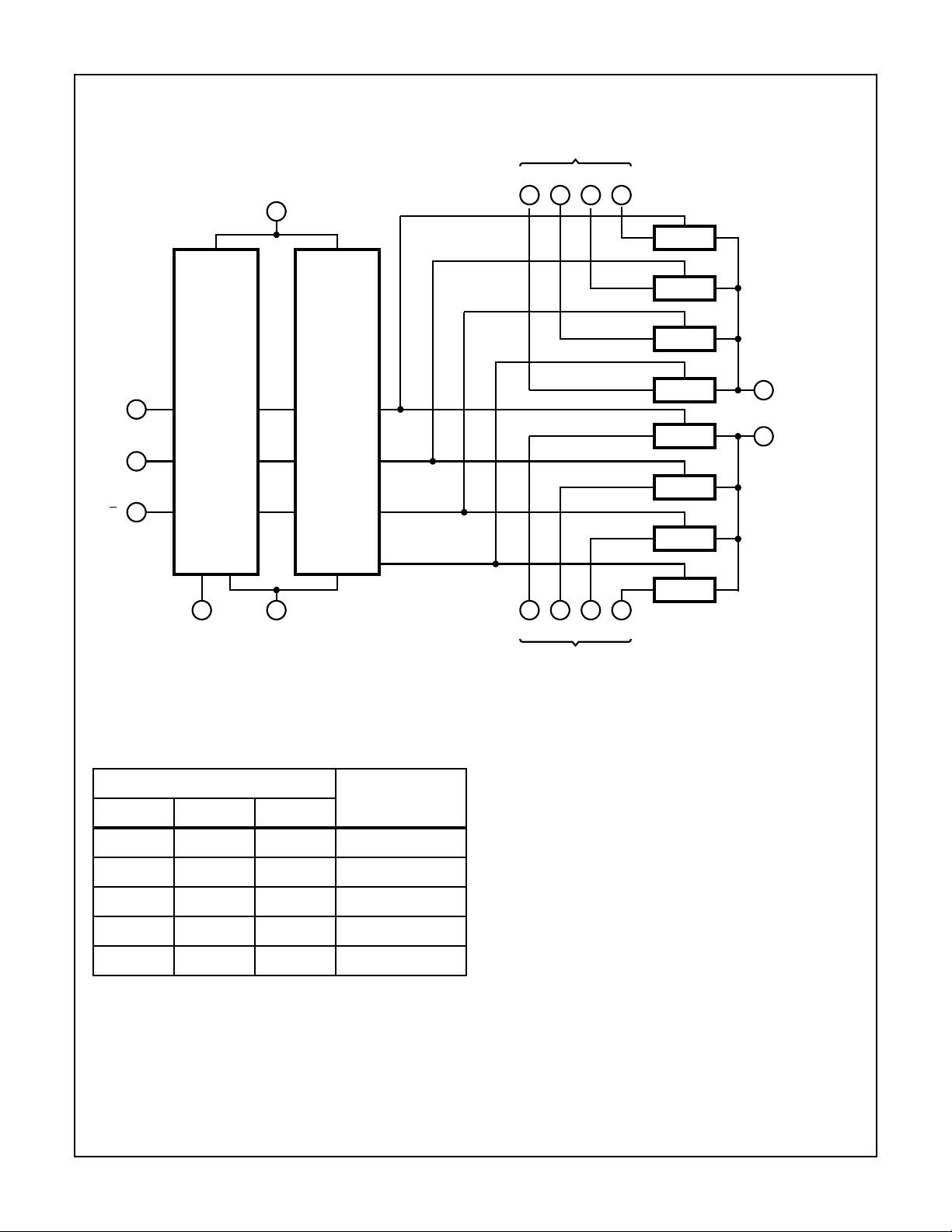
’HC4051, ’HCT4051, ’HC4052, CD74HCT4052, ’HC4053, CD74HCT4053’HC4051, ’HCT4051, ’HC4052, CD74HCT4052, ’HC4053, CD74HCT4053
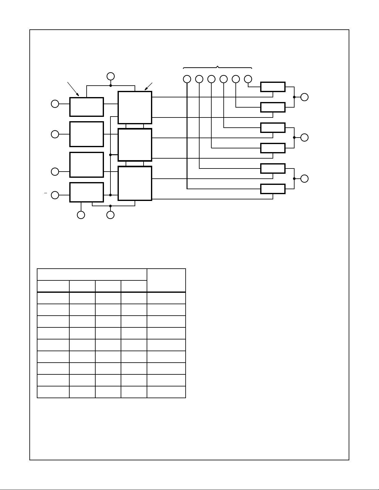
Functional Diagram of ’HC4053, CD74HCT4053
LOGIC LEVEL
CONVERSION
11
S
0
10
S
1
S
9
2
6E
8
GND V
V
CC
16
7
EE
BINARY TO
1 OF 2
DECODERS
WITH ENABLE
C1C0B1B0A1A
IN/OUT
0
12132153
TG
A COMMON
14
OUT/IN
TG
TG
B COMMON
15
OUT/IN
TG
TG
C COMMON
4
OUT/IN
TG
TRUTH TABLE
’HC4053, CD74HCT4053
INPUT STATES
0
S
1
S
2
L L L L C0, B0, A0
L H L L C0, B0, A1
L L H L C0, B1, A0
L H H L C0, B1, A1
L L L H C1, B0, A0
L H L H C1, B0, A1
L L H H C1, B1, A0
L H H H C1, B1, A1
H X X X None
X = Don’t care
“ON”
CHANNELSENABLE S
5
’HC4051, ’HCT4051, ’HC4052, CD74HCT4052, ’HC4053, CD74HCT4053’HC4051, ’HCT4051, ’HC4052, CD74HCT4052, ’HC4053, CD74HCT4053
Absolute Maximum Ratings (Note 2) Thermal Information
DC Supply Voltage, VCC - VEE . . . . . . . . . . . . . . . . . -0.5V to 10.5V
DC Supply Voltage, V
DC Supply Voltage, V
DC Input Diode Current, I
CC. . . . . . . . . . . . . . . . . . . . . . . . . . . . -0.5V to +7V
EE . . . . . . . . . . . . . . . . . . . . . . . . . . . . +0.5V to -7V
IK
For VI < -0.5V or VI > VCC + 0.5V. . . . . . . . . . . . . . . . . . . . . .±20mA
DC Switch Diode Current, I
OK
For VI < VEE -0.5V or VI > VCC + 0.5V . . . . . . . . . . . . . . . . .±20mA
DC Switch Current, (Note 2)
For VI > VEE -0.5V or VI < VCC + 0.5V . . . . . . . . . . . . . . . . .±25mA
DC VCC or Ground Current, ICC . . . . . . . . . . . . . . . . . . . . . . . . .±50mA
DC VEE Current, IEE . . . . . . . . . . . . . . . . . . . . . . . . . . . . . . . -20mA
NOTE:
1. The package thermal impedance is calculated in accordance with JESD 51-7.
Recommended Operating Conditions For maximum reliability, nominal operating conditions should be selected so that
operation is always within the following ranges
PARAMETER MIN MAX UNITS
Supply Voltage Range (For TA = Full Package Temperature Range), VCC (Note 2)
CD54/74HC Types 26V
CD54/74HCT Types 4.5 5.5 V
Supply Voltage Range (For TA = Full Package Temperature Range), VCC - V
CD54/74HC Types, CD54/74HCT Types (See Figure 1) 2 10 V
Supply Voltage Range (For TA = Full Package Temperature Range), VEE (Note 3)
CD54/74HC Types, CD54/74HCT Types (See Figure 2) 0 -6 V
DC Input Control Voltage, V
Analog Switch I/O Voltage, V
Operating Temperature, T
Input Rise and Fall Times, tr, t
2V 0 1000 ns
4.5V 0 500 ns
6V 0 400 ns
CAUTION: Stresses abovethose listed in “Absolute Maximum Ratings” may cause permanent damage to the device.This is a stress only rating and operation
of the device at these or any other conditions above those indicated in the operational sections of this specification is not implied.
NOTES:
2. All voltages referenced to GND unless otherwise specified..
3. Incertain applications, the external load resistor current may includeboth VCCandsignal line components. To avoid drawing VCCcurrent
when switch current flows into the transmission gate inputs, the voltage drop across the bidirectional switch must not exceed 0.6V (calculated from rONvalues shown in Electrical Specifications table). No VCCcurrent will flow through RLif the switch current flows into
terminal 3 on the HC/HCT4051; terminals 3 and 13 on the HC/HCT4052; terminals 4, 14 and 15 on the HC/HCT4053.
I
IS
A
f
Package Thermal Impedance, θJA(see Note 1):
E (PDIP) Package . . . . . . . . . . . . . . . . . . . . . . . . . . . . . . .67oC/W
M (SOIC) Package. . . . . . . . . . . . . . . . . . . . . . . . . . . . . . .73oC/W
NS (SOP) Package . . . . . . . . . . . . . . . . . . . . . . . . . . . . . .64oC/W
PW (TSSOP) Package . . . . . . . . . . . . . . . . . . . . . . . . . .108oC/W
Maximum Junction Temperature. . . . . . . . . . . . . . . . . . . . . . . 150oC
Maximum Storage Temperature Range . . . . . . . . . .-65oC to 150oC
Maximum Lead Temperature (Soldering 10s). . . . . . . . . . . . . 300oC
EE
GND V
V
EE
V
-55 125
CC
CC
V
V
o
C
Recommended Operating Area as a Function of Supply Voltages
8
6
HC
4
- GND (V)
CC
2
V
0
024681012
VCC - VEE (V)
FIGURE 1. FIGURE 2.
HCT
6
8
6
4
- GND (V)
CC
2
V
0
0-2-4-6-8
HCT
VEE - GND (V)
HC
’HC4051, ’HCT4051, ’HC4052, CD74HCT4052, ’HC4053, CD74HCT4053’HC4051, ’HCT4051, ’HC4052, CD74HCT4052, ’HC4053, CD74HCT4053
DC Electrical Specifications
TEST CONDITIONS AMBIENT TEMPERATURE, T
25oC -40oC - 85oC -55oC - 125oC
MIN TYP MAX MIN MAX MIN MAX
PARAMETER
V
(V)
V
V
IS
I
(V)
(V)
EE
V
CC
(V)
HC TYPES
High Level Input Voltage,
V
IH
2 1.5 - - 1.5 - 1.5 - V
4.5 3.15 - - 3.15 - 3.15 0 V
6 4.2 - - 4.2 - 4.2 - V
Low Level Input Voltage,
V
IL
2 - - 0.5 - 0.5 - 0.5 V
4.5 - - 1.35 - 1.35 - 1.35 V
6 - - 1.8 - 1.8 - 1.8 V
On Resistance, r
ON
IO = 1mA, (Figure 11)
VCC or V
EE
VIL or
V
IH
0 4.5 - 70 160 - 200 - 240 Ω
0 6 - 60 140 - 175 - 210 Ω
-4.5 4.5 - 40 120 - 150 - 180 Ω
VCC to V
EE
0 4.5 - 90 180 - 225 - 270 Ω
0 6 - 80 160 - 200 - 240 Ω
-4.5 4.5 - 45 130 - 162 - 195 Ω
Maximum On Resistance
Between any Two
Channels, ∆r
ON
04.5-10-----Ω
06-8.5-----Ω
-4.5 4.5 - 5 - ----Ω
Switch On/Off Leakage
Current, I
IZ
1 and 2 Channels 0 6 - - ±0.1 - ±1-±1 µA
4053 -5 5 - - ±0.1 - ±1-±1 µA
For Switch Off:
When VIS=VCC,
VOS = VEE;
When VIS=VEE,
VOS = V
CC
VIL or
V
IH
For Switch On:
4 Channels 0 6 - - ±0.1 - ±1-±1 µA
4052 -5 5 - - ±0.2 - ±2-±2 µA
8 Channels 0 6 - - ±0.2 - ±2-±2 µA
All Applicable
Combinations of
VIS and V
OS
Voltage Levels
4051 -5 5 - - ±0.4 - ±4-±4 µA
Control Input Leakage
Current, I
IL
Quiescent Device
Current, I
CC
IO = 0
When VIS=VEE,
VOS = V
CC
When VIS=VCC,
VOS = V
EE
VCC or
GND
VCC or
GND
06 - -±0.1 - ±1-±1 µA
0 6 - - 8 - 80 - 160 µA
-5 5 - - 16 - 160 - 320 µA
A
UNITS
7

’HC4051, ’HCT4051, ’HC4052, CD74HCT4052, ’HC4053, CD74HCT4053’HC4051, ’HCT4051, ’HC4052, CD74HCT4052, ’HC4053, CD74HCT4053
DC Electrical Specifications (Continued)
TEST CONDITIONS AMBIENT TEMPERATURE, T
25oC -40oC - 85oC -55oC - 125oC
MIN TYP MAX MIN MAX MIN MAX
PARAMETER
V
(V)
V
V
IS
I
(V)
(V)
EE
V
CC
(V)
HCT TYPES
High Level Input Voltage,
V
IH
Low Level Input Voltage,
V
IL
On Resistance, r
ON
IO = 1mA, (Figure 15)
VCC or V
EE
VIL or
V
IH
4.5to
2--2-2-V
5.5
4.5to
- - 0.8 - 0.8 - 0.8 V
5.5
0 4.5 - 70 160 - 200 - 240 Ω
---------Ω
-4.5 4.5 - 40 120 - 150 - 180 Ω
VCC to V
EE
0 4.5 - 90 180 - 225 - 270 Ω
---------Ω
-4.5 4.5 - 45 130 - 162 - 195 Ω
Maximum On Resistance
Between any Two
Channels, ∆r
ON
04.5-10-----Ω
---------Ω
-4.5 4.5 - 5 - ----Ω
Switch On/Off Leakage
Current, I
IZ
1 and 2 Channels 0 6 - - ±0.1 - ±1-±1 µA
4053 -5 5 - - ±0.1 - ±1-±1 µA
For Switch Off:
When VIS=VCC,
VOS = VEE;
When VIS=VEE,
VOS = V
CC
VIL or
V
IH
For Switch On:
4 Channels 0 6 - - ±0.1 - ±1-±1 µA
4052 -5 5 - - ±0.2 - ±2-±2 µA
8 Channels 0 6 - - ±0.2 - ±2-±2 µA
All Applicable
Combinations of
VIS and V
OS
Voltage Levels
4051 -5 5 - - ±0.4 - ±4-±4 µA
Control Input Leakage
Current, I
IL
Quiescent Device
Current, I
CC
IO = 0
Additional Quiescent
Device Current
- (Note 4) - 5.5 - - ±0.1 - ±1-±1 µA
When VIS=VEE,
VOS = V
CC
When VIS=VCC,
VOS = V
EE
∆ICC
(Note 5)
VCC or
GND
VCC -
2.1
0 5.5 - - 8 - 80 - 160 µA
-4.5 5.5 - - 16 - 160 - 320 µA
4.5to
- 100 360 - 450 - 490 µA
5.5
Per Input Pin: 1 Unit
Load
NOTES:
4. Any voltage between VCC and GND.
5. For dual supply systems theoretical worst case (VI = 2.4V, VCC = 5.5V) specification is 1.8mA.
A
UNITS
HCT Input Loading Table
UNIT LOADS
TYPE INPUT
4051, 4053 All 0.5
4052 All 0.4
NOTE: Unit load is ∆ICC limit specified in DC Specifications table,
e.g., 360mA max. at 25oC.
(NOTE)
8

’HC4051, ’HCT4051, ’HC4052, CD74HCT4052, ’HC4053, CD74HCT4053’HC4051, ’HCT4051, ’HC4052, CD74HCT4052, ’HC4053, CD74HCT4053
Switching Specifications V
= 5V, TA = 25oC, Input tr, tr = 6ns
CC
TYPICAL
4051 4052 4053
C
PARAMETER
(pF)
L
HC HCT HC HCT HC HCT
Propagation Delay
Switch IN to OUT, t
Switch Turn-Off (S or E), t
Switch Turn-On (S or E), t
PHL
, t
PLH
PHZ,tPLZ
PZH
15444444ns
15 19 19 21 21 18 18 ns
, t
PZL
15 19 23 27 29 18 20 ns
Power Dissipation Capacitance, CPD (Note 6) - 50 52 74 76 38 42 pF
NOTE:
6. CPD is used to determine the dynamic power consumption, per package.
PD = CPD V
2
fI + ∑ (CL + CS) V
CC
CC
2
f
O
fO = output frequency
fI = input frequency
CL = output load capacitance
CS = switch capacitance
VCC = supply voltage
Switching Specifications C
= 50pF, Input tr, tr = 6ns
L
AMBIENT TEMPERATURE, T
A
25oC -40oC - 85oC -55oC - 125oC
UNITS
PARAMETER
Propagation Delay, Switch
In to Out, t
Maximum Switch
PLH
, t
PHL
4051 0 2 - 225 - - - 280 - - - 340 - - ns
Turn “Off” Delay
from S or E to
Switch Output
t
, t
PHZ
PLZ
4052 0 2 - 250 - - - 315 - - - 375 - - ns
4053 0 2 - 210 - - - 265 - - - 315 - - ns
V
V
EE
CC
(V)
(V)
MIN MAX MIN MAX MIN MAX MIN MAX MIN MAX MIN MAX
UNITS
02-60---75---90--ns
0 4.5 - 12 - 12 - 15 - 15 - 18 - 18 ns
06-10---13---15--ns
-4.5 4.5 - 8 - 8 - 10 - 10 - 12 - 12 ns
0 4.5 - 45 - 45 - 56 - 56 - 68 - 68 ns
06-38---48---57--ns
-4.5 4.5 - 32 - 32 - 40 - 40 - 48 - 48 ns
0 4.5 - 50 - 50 - 63 - 63 - 75 - 75 ns
06-43---54---65--ns
-4.5 4.5 - 38 - 38 - 48 - 48 - 57 - 57 ns
0 4.5 - 42 - 44 - 53 - 55 - 63 - 66 ns
HC HCT HC HCT HC HCT
06-36---45---54--ns
-4.5 4.5 - 29 - 31 - 36 - 39 - 44 - 47 ns
9

’HC4051, ’HCT4051, ’HC4052, CD74HCT4052, ’HC4053, CD74HCT4053’HC4051, ’HCT4051, ’HC4052, CD74HCT4052, ’HC4053, CD74HCT4053
Switching Specifications C
V
PARAMETER
Maximum Switch
Turn “On” Delay
from S or E to
Switch Output
t
, t
PZL
PZH
4051 0 2 - 225 - - - 280 - - - 340 - - ns
4052 0 2 - 325 - - - 405 - - - 490 - - ns
4053 0 2 - 220 - - - 275 - - - 330 - - ns
EE
(V)
0 4.5 - 45 - 55 - 56 - 69 - 68 - 83 ns
06-38---48---57--ns
-4.5 4.5 - 32 - 39 - 40 - 49 - 48 - 59 ns
0 4.5 - 65 - 70 - 81 - 68 - 98 - 105 ns
06-55---69---83--ns
-4.5 4.5 - 46 - 48 - 58 - 60 - 69 - 72 ns
0 4.5 - 44 - 48 - 55 - 60 - 66 - 72 ns
06-37---47---56--ns
= 50pF, Input tr, tr = 6ns (Continued)
L
AMBIENT TEMPERATURE, T
A
25oC -40oC - 85oC -55oC - 125oC
HC HCT HC HCT HC HCT
V
CC
(V)
MIN MAX MIN MAX MIN MAX MIN MAX MIN MAX MIN MAX
UNITS
-4.5 4.5 - 31 - 34 - 39 - 43 - 47 - 51 ns
Input (Control)
Capacitance, C
I
- - - 10 - 10 - 10 - 10 - 10 - 10 pF
Analog Channel Specifications Typical Values at T
PARAMETER TEST CONDITIONS
Switch Input Capacitance, C
Common Output Capacitance, C
Minimum Switch Frequency Response at -3dB, f
(Figures 12, 14, 16)
I
COM
MAX
See Figure 3 (Notes 7, 8) 4051
= 25oC
A
HC/HCT
TYPES
V
(V)
EE
V
(V)
CC
HC/
HCT UNITS
All - - 5 pF
4051 - - 25 pF
4052 - - 12 pF
4053 - - 8 pF
145 MHz
4052 165 MHz
-2.25 2.25
4053 200 MHz
4051
4052 185 MHz
-4.5 4.5
180 MHz
4053 200 MHz
10

’HC4051, ’HCT4051, ’HC4052, CD74HCT4052, ’HC4053, CD74HCT4053’HC4051, ’HCT4051, ’HC4052, CD74HCT4052, ’HC4053, CD74HCT4053
Analog Channel Specifications Typical Values at T
PARAMETER TEST CONDITIONS
Crosstalk Between any Two Switches (Note 10) See Figure 4
Sinewave Distortion See Figure 5 All -2.25 2.25 0.035 %
E or S to Switch Feedthrough Noise See Figure 6
Switch “OFF” Signal Feedthrough (Figures 13, 15, 17) See Figure 7
NOTES:
7. Adjust input voltage to obtain 0dBm at VOS for fIN = 1MHz.
8. VIS is centered at (VCC - VEE)/2.
9. Adjust input for 0dBm.
10. Not applicable for HC/HCT4051.
= 25oC
A
(Notes 8, 9)
(Notes 8, 9)
(Notes 8, 9)
HC/HCT
TYPES
4051
4052 (TBE) dB
4053 (TBE) dB
4051
4052 (TBE) dB
4053 (TBE) dB
All -4.5 4.5 0.018 %
4051
4052 mV
4053 mV
4051
4052 mV
4053 mV
4051
4052 -65 dB
4053 -64 dB
4051
4052 -67 dB
4053 -66 dB
V
EE
(V)
-2.25 2.25
-4.5 4.5
-2.25 2.25 (TBE)
-4.5 4.5 (TBE)
-2.25 2.25
-4.5 4.5
V
(V)
CC
HC/
HCT UNITS
N/A dB
N/A dB
-73 dB
-75 dB
mV
mV
11

’HC4051, ’HCT4051, ’HC4052, CD74HCT4052, ’HC4053, CD74HCT4053
Test Circuits and Waveforms
V
IS
CC
SWITCH
ON
R
VCC/2
VCC/2
R
V
OS2
C
V
R
INPUT
V
CC
f
R = 50Ω
0.1µF
= 1MHz SINEWAVE
IS
C = 10pF
V
10pF
OS
dB
METER
V
CC
R
SWITCH
OFF
V
/2
CC
V
IS
0.1µF
SWITCH
ON
50Ω
/2
V
CC
FIGURE 3. FREQUENCY RESPONSE TEST CIRCUIT FIGURE 4. CROSSTALKBETWEEN TWO SWITCHES TEST
CIRCUIT
C
METER
dB
V
OS1
E
V
CC
SWITCH
ALTERNATING
ON AND OFF
, tf≤ 6ns
t
r
= 1MHz
f
CONT
50% DUTY
CYCLE
VCC/2
600Ω
V
OS
V
50pF
SINE-
WAVE
10µF
V
IS
fIS = 1kHz TO 10kHz
V
CC
SWITCH
ON
= V
V
I
10kΩ
IH
50pF
V
IS
V
OS
DISTORTION
600Ω
VCC/2
METER
/2
V
CC
FIGURE 5. SINEWAVE DISTORTION TEST CIRCUIT FIGURE 6. CONTROL TO SWITCH FEEDTHROUGH NOISE
TEST CIRCUIT
fIS≥ 1MHz SINEWAVE
V
CC
= V
V
0.1µF
V
IS
SWITCH
OFF
C
R
VCC/2
VCC/2
R = 50Ω
C = 10pF
IL
R
V
OS
C
dB
METER
OS
SCOPE
V
P-P
FIGURE 7. SWITCH OFF SIGNAL FEEDTHROUGH
12

’HC4051, ’HCT4051, ’HC4052, CD74HCT4052, ’HC4053, CD74HCT4053
Test Circuits and Waveforms (Continued)
= 6ns tf = 6ns
t
r
SWITCH INPUT
90%
50%
10%
V
CC
SWITCH OUTPUT
6ns 6ns
E OR Sn
50%
t
PLZ
90%
OUTPUT LOW
TO OFF
OUTPUT HIGH
t
PHZ
10%
90%
TO OFF
SWITCH ON
FIGURE 8B. HC TYPES FIGURE 8C. HCT TYPES
FIGURE 8. SWITCH PROPAGATION DELAY, TURN-ON, TURN-OFF TIMES
10%
t
t
PZH
PZL
t
PLH
50%
50%
SWITCH ONSWITCH OFF
FIGURE 8A.
V
CC
GND
E OR Sn
OUTPUT LOW
OUTPUT HIGH
t
PHL
V
EE
90%
50%
10%
6ns 6ns
t
r
1.3
t
PLZ
TO OFF
t
PHZ
10%
90%
t
2.7
f
0.3
t
PZL
t
PZH
TO OFF
SWITCH ON
3V
GND
50%
50%
SWITCH ONSWITCH OFF
OUT
VCC FOR
t
AND t
PLZ
V
FOR
EE
t
AND t
PHZ
PZL
PZH
t
t
PHZ
PLZ
VEE FOR
AND t
V
FOR
CC
AND t
PZL
PZH
= 1kΩ
R
TG
IN
L
C
L
50pF
FIGURE 9. SWITCH ON/OFF PROPAGATION DELAY TEST
CIRCUIT
IN
TG
OUT
50pF
FIGURE 10. SWITCH IN TO SWITCH OUT PROPAGATION
DELAY TEST CIRCUIT
13

’HC4051, ’HCT4051, ’HC4052, CD74HCT4052, ’HC4053, CD74HCT4053
Typical Performance Curves
120
100
80
60
40
ON RESISTANCE (Ω)
20
VCC - VEE = 4.5V
VCC - VEE = 6V
VCC - VEE = 9V
123456789
INPUT SIGNAL VOLTAGE (V)
FIGURE 11. TYPICAL ON RESISTANCE vs INPUT SIGNAL VOLTAGE
0
VCC = 4.5V
-2
-4
dB
-6
-8
-10
10K 100K 1M 10M 100M
GND = -4.5V
= -4.5V
V
EE
= 50Ω
R
L
PIN 12 TO 3
FREQUENCY (Hz)
VCC = 2.25V
GND = -2.25V
= -2.25V
V
EE
= 50Ω
R
L
PIN 12 TO 3
0
-20
-40
dB
-60
-80
-100
10K 100K
VCC = 2.25V
GND = -2.25V
= -2.25V
V
EE
= 50Ω
R
L
PIN 12 TO 3
1M
FREQUENCY (Hz)
VCC = 4.5V
GND = -4.5V
= -4.5V
V
EE
= 50Ω
R
L
PIN 12 TO 3
10M 100M
FIGURE 12. CHANNEL ON BANDWIDTH (HC/HCT4051) FIGURE 13. CHANNEL OFF FEEDTHROUGH (HC/HCT4051)
0
VCC = 4.5V
-2
-4
dB
-6
-8
-10
10K 100K 1M 10M 100M
FREQUENCY (Hz)
GND = -4.5V
= -4.5V
V
EE
= 50Ω
R
L
PIN 4 TO 3
VCC = 2.25V
GND = -2.25V
= -2.25V
V
EE
= 50Ω
R
L
PIN 4 TO 3
0
VCC = 2.25V
-20
-40
dB
-60
-80
-100
10K 100K 1M 10M 100M
FREQUENCY (Hz)
GND = -2.25V
= -2.25V
V
EE
= 50Ω
R
L
PIN 4 TO 3
VCC = 4.5V
GND = -4.5V
= -4.5V
V
EE
= 50Ω
R
L
PIN 4 TO 3
FIGURE 14. CHANNEL ON BANDWIDTH (HC/HCT4052) FIGURE 15. CHANNEL OFF FEEDTHROUGH (HC/HCT4052)
14

’HC4051, ’HCT4051, ’HC4052, CD74HCT4052, ’HC4053, CD74HCT4053
Typical Performance Curves (Continued)
0
0
-1
-2
dB
-3
-4
10K 100K 1M 10M 100M
FREQUENCY (Hz)
VCC = 4.5V
GND = -4.5V
= -4.5V
V
EE
= 50Ω
R
L
PIN 5 TO 4
VCC = 2.25V
GND = -2.25V
= -2.25V
V
EE
= 50Ω
R
L
PIN 5 TO 4
-20
-40
dB
-60
-80
-100
10K 100K 1M 10M 100M
FIGURE 16. CHANNEL ON BANDWIDTH (HC/HCT4053) FIGURE 17. CHANNEL OFF FEEDTHROUGH (HC/HCT4053)
VCC = 2.25V
GND = -2.25V
= -2.25V
V
EE
R
= 50Ω
L
PIN 5 TO 4
FREQUENCY (Hz)
VCC = 4.5V
GND = -4.5V
= -4.5V
V
EE
= 50Ω
R
L
PIN 5 TO 4
15


MECHANICAL
MPDI002C – JANUARY 1995 – REVISED DECEMBER 20002
N (R-PDIP-T**) PLASTIC DUAL-IN-LINE PACKAGE
16 PINS SHOWN
16
1
0.045 (1,14)
0.030 (0,76)
A
0.070 (1,78)
0.045 (1,14)
D
9
8
D
0.020 (0,51) MIN
0.260 (6,60)
0.240 (6,10)
0.200 (5,08) MAX
0.125 (3,18) MIN
DIM
A MAX
A MIN
C
Seating Plane
MS-100
VARIATION
PINS **
14
0.775
(19,69)
0.745
(18,92)
AA
0.325 (8,26)
0.300 (7,62)
16
0.775
(19,69)
0.745
(18,92)
BB AC AD
18
0.920
(23,37)
0.850
(21,59)
0.015 (0,38)
Gauge Plane
0.010 (0,25) NOM
20
1.060
(26,92)
0.940
(23,88)
0.100 (2,54)
0.021 (0,53)
0.015 (0,38)
0.010 (0,25)
NOTES: A. All linear dimensions are in inches (millimeters).
B. This drawing is subject to change without notice.
C. Falls within JEDEC MS-001, except 18 and 20 pin minimum body lrngth (Dim A).
D. The 20 pin end lead shoulder width is a vendor option, either half or full width.
M
14/18 PIN ONLY
20 pin vendor option
0.430 (10,92) MAX
D
4040049/E 12/2002
POST OFFICE BOX 655303 • DALLAS, TEXAS 75265
1

MECHANICAL DATA
MSOI002B – JANUARY 1995 – REVISED SEPTEMBER 2001
D (R-PDSO-G**) PLASTIC SMALL-OUTLINE PACKAGE
8 PINS SHOWN
8 5
1 4
A
0.069 (1,75) MAX
0.020 (0,51)
0.014 (0,35)
0.157 (4,00)
0.150 (3,81)
0.010 (0,25)
0.004 (0,10)
0.244 (6,20)
0.228 (5,80)
0.010 (0,25)0.050 (1,27)
0.008 (0,20) NOM
Gage Plane
0.010 (0,25)
0°– 8°
0.044 (1,12)
0.016 (0,40)
Seating Plane
0.004 (0,10)
PINS **
DIM
A MAX
A MIN
NOTES: A. All linear dimensions are in inches (millimeters).
B. This drawing is subject to change without notice.
C. Body dimensions do not include mold flash or protrusion, not to exceed 0.006 (0,15).
D. Falls within JEDEC MS-012
8
0.197
(5,00)
0.189
(4,80)
14
0.344
(8,75)
0.337
(8,55)
16
0.394
(10,00)
0.386
(9,80)
4040047/E 09/01
POST OFFICE BOX 655303 • DALLAS, TEXAS 75265
1


MECHANICAL DATA
MSSO002E – JANUARY 1995 – REVISED DECEMBER 2001
DB (R-PDSO-G**) PLASTIC SMALL-OUTLINE
28 PINS SHOWN
0,65
28
1
2,00 MAX
0,38
0,22
15
14
A
0,05 MIN
0,15
5,60
5,00
M
8,20
7,40
Seating Plane
0,10
0,25
0,09
0°–ā8°
Gage Plane
0,25
0,95
0,55
PINS **
DIM
A MAX
A MIN
NOTES: A. All linear dimensions are in millimeters.
B. This drawing is subject to change without notice.
C. Body dimensions do not include mold flash or protrusion not to exceed 0,15.
D. Falls within JEDEC MO-150
14
6,50
6,50
5,905,90
2016
7,50
6,90
24
8,50
28
10,50
9,907,90
30
10,50
9,90
38
12,90
12,30
4040065 /E 12/01
POST OFFICE BOX 655303 • DALLAS, TEXAS 75265
1

MECHANICAL DATA
MTSS001C – JANUARY 1995 – REVISED FEBRUARY 1999
PW (R-PDSO-G**) PLASTIC SMALL-OUTLINE PACKAGE
14 PINS SHOWN
0,65
1,20 MAX
14
0,30
0,19
8
4,50
4,30
PINS **
7
Seating Plane
0,15
0,05
8
1
A
DIM
6,60
6,20
14
0,10
M
0,10
0,15 NOM
0°–8°
2016
Gage Plane
24
0,25
0,75
0,50
28
A MAX
A MIN
NOTES: A. All linear dimensions are in millimeters.
B. This drawing is subject to change without notice.
C. Body dimensions do not include mold flash or protrusion not to exceed 0,15.
D. Falls within JEDEC MO-153
3,10
2,90
5,10
4,90
5,10
4,90
6,60
6,40
7,90
7,70
9,80
9,60
4040064/F 01/97
POST OFFICE BOX 655303 • DALLAS, TEXAS 75265
1

IMPORTANT NOTICE
Texas Instruments Incorporated and its subsidiaries (TI) reserve the right to make corrections, modifications,
enhancements, improvements, and other changes to its products and services at any time and to discontinue
any product or service without notice. Customers should obtain the latest relevant information before placing
orders and should verify that such information is current and complete. All products are sold subject to TI’s terms
and conditions of sale supplied at the time of order acknowledgment.
TI warrants performance of its hardware products to the specifications applicable at the time of sale in
accordance with TI’s standard warranty . Testing and other quality control techniques are used to the extent TI
deems necessary to support this warranty . Except where mandated by government requirements, testing of all
parameters of each product is not necessarily performed.
TI assumes no liability for applications assistance or customer product design. Customers are responsible for
their products and applications using TI components. T o minimize the risks associated with customer products
and applications, customers should provide adequate design and operating safeguards.
TI does not warrant or represent that any license, either express or implied, is granted under any TI patent right,
copyright, mask work right, or other TI intellectual property right relating to any combination, machine, or process
in which TI products or services are used. Information published by TI regarding third–party products or services
does not constitute a license from TI to use such products or services or a warranty or endorsement thereof.
Use of such information may require a license from a third party under the patents or other intellectual property
of the third party , or a license from TI under the patents or other intellectual property of TI.
Reproduction of information in TI data books or data sheets is permissible only if reproduction is without
alteration and is accompanied by all associated warranties, conditions, limitations, and notices. Reproduction
of this information with alteration is an unfair and deceptive business practice. TI is not responsible or liable for
such altered documentation.
Resale of TI products or services with statements different from or beyond the parameters stated by TI for that
product or service voids all express and any implied warranties for the associated TI product or service and
is an unfair and deceptive business practice. TI is not responsible or liable for any such statements.
Following are URLs where you can obtain information on other Texas Instruments products & application
solutions:
Products Applications
Amplifiers amplifier.ti.com Audio www.ti.com/audio
Data Converters dataconverter.ti.com Automotive www.ti.com/automotive
DSP dsp.ti.com Broadband www.ti.com/broadband
Interface interface.ti.com Digital Control www.ti.com/digitalcontrol
Logic logic.ti.com Military www.ti.com/military
Power Mgmt power.ti.com Optical Networking www.ti.com/opticalnetwork
Microcontrollers microcontroller.ti.com Security www.ti.com/security
Telephony www.ti.com/telephony
Video & Imaging www.ti.com/video
Wireless www.ti.com/wireless
Mailing Address: Texas Instruments
Post Office Box 655303 Dallas, Texas 75265
Copyright 2003, Texas Instruments Incorporated
 Loading...