

Siemens 7SR242 User Manual
7SR242 Duobias Description Of Operation
The copyright and other intellectual property rights in this document, and in any model or article produced from it
(and including any registered or unregistered design rights) are the property of Siemens Protection Devices
Limited. No part of this document shall be reproduced or modified or stored in another form, in any data retrieval
system, without the permission of Siemens Protection Devices Limited, nor shall any model or article be
reproduced from this document unless Siemens Protection Devices Limited consent.
While the information and guidance given in this document is believed to be correct, no liability shall be accepted
for any loss or damage caused by any error or omission, whether such error or omission is the result of
negligence or any other cause. Any and all such liability is disclaimed.
©2010 Siemens Protection Devices Limited
7SR242 Duobias
Multi-Function 2-Winding Transformer Protection Relay
Document Release History
This document is issue 2010/06. The list of revisions up to and including this issue is:
2010/06 Additional Comms modules option of (RS485 + IRIG-B) and (RS232 + IRIG-B) and typographical
revisions
2010/02 Document reformat due to rebrand
2010/02 Third issue. Software revision 2662H80001 R4c-3
2008/07 Second issue. Software revision 2662H80001R3d-2c.
2008/05 First issue
Software Revision History
2010/02 2662H80001 R4c-3 Revisions to: VT ratio settings, 87BD 1st bias slope limit setting
increments, CB fail function, LED CONFIG menu, DATA
STORAGE menu.
Added: Open circuit detection (46BC), CONTROL MODE
menu, Close circuit supervision (74CCS), Measured earth fault
undercurrent (37G), Pulsed output contacts.
2008/07 2662H80001R3d-2c. Demand metering. Optional DNP3.0 data comms.
2008/05 2662H80001R3-2b First Release

7SR242 Duobias Description Of Operation
©2010 Siemens Protection Devices Limited Chapter 1 Page 2 of 52
Contents
Section 1: Introduction..........................................................................................................................6
Current Transformer Circuits ............................................................................................................6
External Resistors.............................................................................................................................6
Fibre Optic Communication ..............................................................................................................6
Front Cover.......................................................................................................................................6
Section 2: Hardware Description........................................................................................................13
2.1 General ...................................................................................................................................13
2.2 Case........................................................................................................................................13
2.3 Front Cover .............................................................................................................................13
2.4 Power Supply Unit (PSU)........................................................................................................14
2.5 Operator Interface/ Fascia ......................................................................................................14
2.6 Current Inputs .........................................................................................................................16
2.7 Voltage Input...........................................................................................................................16
2.8 Binary inputs ...........................................................................................................................17
2.9 Binary outputs (Output Relays)...............................................................................................18
2.10 Virtual Input/Outputs ...............................................................................................................19
2.11 Self Monitoring ........................................................................................................................19
2.11.1 Protection Healthy/Defective......................................................................................19
Section 3: Protection Functions.........................................................................................................20
3.1 Current Protection: Differential Protection ..............................................................................20
3.1.1 ICT..............................................................................................................................20
3.1.2 Overall Biased Differential (87BD) .............................................................................21
3.1.3 87HS ..........................................................................................................................23
3.2 Current Protection: Phase Overcurrent (51, 50) .....................................................................25
3.2.1 Instantaneous Overcurrent Protection (50)................................................................25
3.2.2 Time Delayed Overcurrent Protection (51) ................................................................26
3.3 Current Protection: Derived Earth Fault (50N, 51N) ...............................................................27
3.3.1 Instantaneous Derived Earth Fault Protection (50N) .................................................27
3.3.2 Time Delayed Derived Earth Fault Protection (51N)..................................................28
3.4 Current Protection: Measured Earth Fault (50G, 51G) ...........................................................29
3.4.1 Instantaneous Measured Earth Fault Protection (50G) .............................................29
3.4.2 Time Delayed Measured Earth Fault Protection (51G)..............................................30
3.5 Current Protection: High Impedance Restricted Earth Fault (64H) ........................................31
3.6 Open Circuit (46BC)................................................................................................................32
3.7 Current Protection: Negative Phase Sequence Overcurrent (46NPS) ...................................33
3.8 Current Protection: Under-Current (37, 37G) .........................................................................34
3.9 Current Protection: Thermal Overload (49) ............................................................................35
3.10 Voltage Protection: Over Fluxing (24).....................................................................................37
3.11 Voltage Protection: Under/Over Voltage (27/59) ....................................................................39
3.12 Voltage Protection: Neutral Overvoltage (59N) ......................................................................40
3.13 Voltage Protection: Under/Over Frequency (81) ....................................................................41
Section 4: Control & Logic Functions................................................................................................42
4.1 Quick Logic .............................................................................................................................42
Section 5: Supervision Functions ......................................................................................................44
5.1 Circuit Breaker Failure (50BF) ................................................................................................44
5.2 Trip/Close Circuit Supervision (74TCS/74CCS) .....................................................................45
5.3 Inrush Detector (81HBL2) .......................................................................................................46

7SR242 Duobias Description Of Operation
©2010 Siemens Protection Devices Limited Chapter 1 Page 3 of 52
5.4 OverFluxing Detector (81HBL5)..............................................................................................46
5.5 Demand...................................................................................................................................47
Section 6: Other Features....................................................................................................................48
6.1 Data Communications.............................................................................................................48
6.2 Maintenance............................................................................................................................48
6.2.1 Output Matrix Test......................................................................................................48
6.2.2 CB Counters...............................................................................................................48
6.2.3 I2t CB Wear ................................................................................................................48
6.3 Data Storage...........................................................................................................................49
6.3.1 General.......................................................................................................................49
6.3.2 Event Records............................................................................................................49
6.3.3 Waveform Records. ...................................................................................................49
6.3.4 Fault Records.............................................................................................................50
6.3.5 Demand/Data Log ......................................................................................................50
6.4 Metering ..................................................................................................................................50
6.5 Operating Mode ......................................................................................................................51
6.6 Control Mode...........................................................................................................................51
6.7 Real Time Clock......................................................................................................................51
6.7.1 Time Synchronisation – Data Comms .......................................................................52
6.7.2 Time Synchronisation – Binary Input .........................................................................52
6.7.3 Time Synchronisation – IRIG-B (Optional).................................................................52
6.8 Settings Groups ......................................................................................................................52
6.9 Password Feature...................................................................................................................52
List of Figures
Figure 1-1 Functional Diagram: 7SR242n-2aAnn-0AA0 Relay.............................................................9
Figure 1-2 Functional Diagram: 7SR242n-2aAnn-0BA0 Relay...........................................................10
Figure 1-3 Functional Diagram: 7SR242n-2aAnn-0CA0 Relay ..........................................................11
Figure 1-4 Connection Diagram: 7SR242 Relay.................................................................................12
Figure 2-1 7SR24 with 3 + 16 LEDs in E8 Case................................................................................14
Figure 2-2 Binary Input Logic .............................................................................................................17
Figure 2-3 Binary Output Logic ..........................................................................................................19
Figure 3-1 Biased Differential Characteristic.......................................................................................21
Figure 3-2 Functional Diagram for Biased Current Differential Protection..........................................22
Figure 3-3 Differential Highset Characteristic .....................................................................................23
Figure 3-4 Logic Diagram: High Set Current Differential Protection ...................................................24
Figure 3-5 Logic Diagram: Instantaneous Over-current Element .......................................................25
Figure 3-6 Logic Diagram: Time Delayed Overcurrent Element .........................................................26
Figure 3-7 Logic Diagram: Instantaneous Derived Earth Fault Element ............................................27
Figure 3-8 Logic Diagram: Derived Time Delayed Earth Fault Protection..........................................28
Figure 3-9 Logic Diagram: Measured Instantaneous Earth-fault Element..........................................29
Figure 3-10 Logic Diagram: Time Delayed Measured Earth Fault Element (51G)...............................30
Figure 3-11 Logic Diagram: High Impedance REF (64H).....................................................................31
Figure 3-12 Logic Diagram: Open Circuit Function (46BC) ..................................................................32
Figure 3-13 Logic Diagram: Negative Phase Sequence Overcurrent (46NPS)....................................33
Figure 3-14 Logic Diagram: Undercurrent Detector (37, 37G)..............................................................34
Figure 3-15 Logic Diagram: Thermal Overload Protection (49)............................................................36
Figure 3-16 Inverse Over-fluxing Characteristic (24IT).........................................................................37
Figure 3-17 Logic Diagram: Overfluxing Elements (24)........................................................................38
Figure 3-18 Logic Diagram: Under/Over Voltage Elements (27/59) .....................................................39
Figure 3-19 Logic Diagram: Neutral Overvoltage Element ...................................................................40
Figure 3-20 Logic Diagram: Under/Over Frequency Detector (81).......................................................41
Figure 4-1 Sequence Diagram showing PU/DO Timers in Quick Logic (Counter Reset
Mode Off) ...........................................................................................................................43
Figure 5-1 Logic Diagram: Circuit Breaker Fail Protection (50BF)......................................................44

7SR242 Duobias Description Of Operation
©2010 Siemens Protection Devices Limited Chapter 1 Page 4 of 52
Figure 5-2 Logic Diagram: Trip Circuit Supervision Feature (74TCS) ................................................45
Figure 5-3 Logic Diagram: Close Circuit Supervision Feature (74CCS).............................................45
Figure 5-4 Logic Diagram: Inrush Detector Feature (81HBL2)...........................................................46
Figure 5-5 Logic Diagram: Overfluxing Detector Feature (81HBL5)...................................................46
List of Tables
Table 1-1: 7SR242 Ordering Options....................................................................................................7
Table 2-1 Summary of 7SR24 Relay Configurations .........................................................................13
Table 6-1 Operation Mode .....................................................................................................................51
7SR242 Duobias Description Of Operation
©2010 Siemens Protection Devices Limited Chapter 1 Page 5 of 52
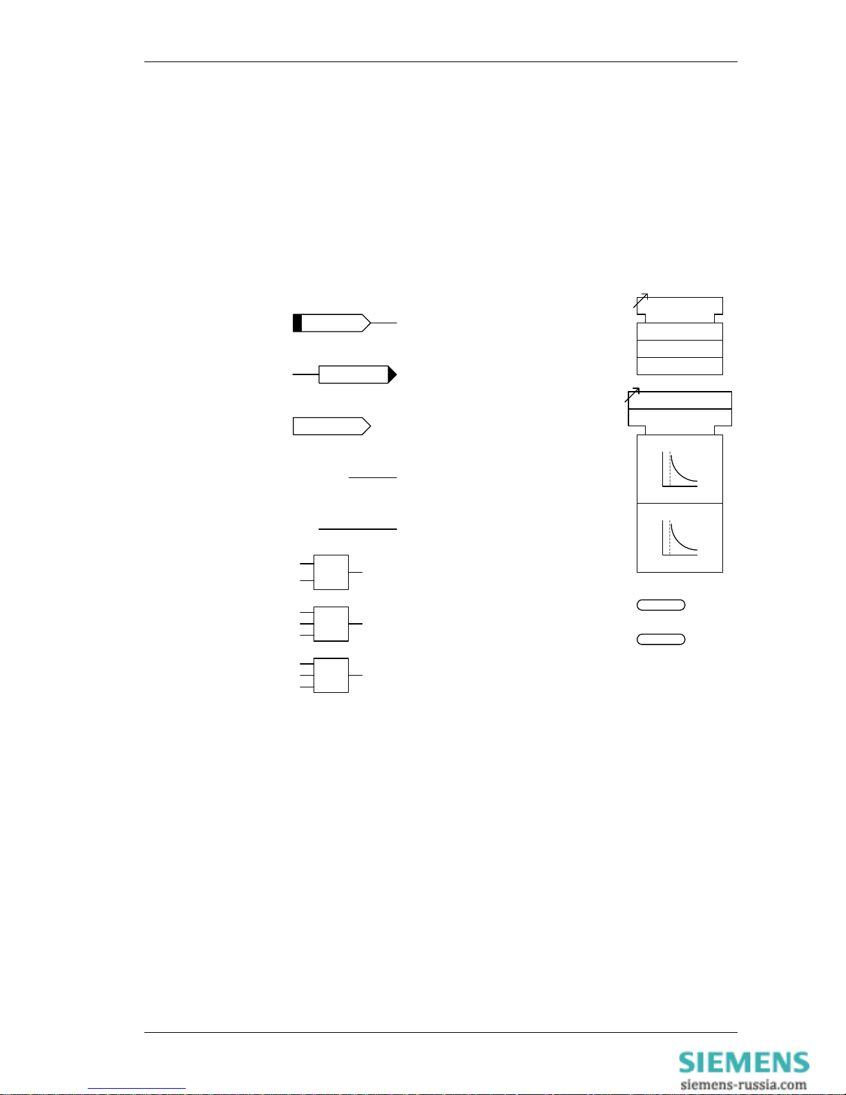
c
start
trip
Elem Starter
Elem Inhibit
Elem Reset Delay
c
Forward
Reverse
Elem Char Dir
Non-Dir
L1 Dir Blk
PhaseAFwd
Binary input signal
visible to user
Binary Output visible to user
Digital signal not visible to
user, to/from another element
List of settings associated with a specific
function
Appropriate list is TRUE when setting
selected.
Digital signal not visible to
user, internal to this element
IL1
Analogue signal with signal
description
Common setting for multiple functions
c
start
trip
Function.
Individual functions are enabled when
associated control input (c) is TRUE.
Common control input (c) for multiple
functions. All functions are enabled
when control input is TRUE.
&
And Gate
(2 inputs shown)
≥1
Or Gate
(3 inputs shown)
INST.
EVENT
EVENT: IEC, Modbus or DNP
Where applicable
Relay instrument
1
Exclusive Or (XOR) Gate
(3 inputs shown)
Symbols and Nomenclature
The following notational and formatting conventions are used within the remainder of this document:
• Setting Menu Location MAIN MENU>SUB-MENU
• Setting: Elem name -Setting
• Setting value: value
• Alternatives: [1st] [2nd] [3rd]
7SR242 Duobias Description Of Operation
©2010 Siemens Protection Devices Limited Chapter 1 Page 6 of 52
Section 1: Introduction
This manual is applicable to the following relays:
• 7SR242 Multi-Function 2-Winding Transformer Protection Relay
The 7SR242 relay integrates the protection and control elements required to provide a complete transformer
protection.
The ‘Ordering Options’ Tables summarise the features available in each model.
General Safety Precautions
Current Transformer Circuits
The secondary circuit of a live CT must not be open circuited. Non-observance of this precaution can result in
injury to personnel or damage to equipment.
External Resistors
Where external resistors are fitted to relays, these may present a danger of electric shock or burns, if touched.
Fibre Optic Communication
Where fibre optic communication devices are fitted, these should not be viewed directly. Optical power meters
should be used to determine the operation or signal level of the device.
Front Cover
The front cover provides additional securing of the relay element within the case. The relay cover should be in
place during normal operating conditions.
!
!
!
!

7SR242 Duobias Description Of Operation
©2010 Siemens Protection Devices Limited Chapter 1 Page 7 of 52
Table 1-1: 7SR242 Ordering Options
DUOBIAS-M 7 S R 2 4 2
□
- 2 □ A □
□
- 0 □ A 0
▲ ▲ ▲ ▲ ▲ ▲ ▲ ▲ ▲
Multifunctional 2 winding
| | |
| | | | | |
transformer differential Protection Product
| | |
| | | | | |
protection Transformer
4
| |
| | | | | |
|
|
| | | | | |
Relay Type
|
|
| | | | | |
Differential (2 winding)
2
|
| | | | | |
|
| | | | | |
Case I/O and Fascia
|
| | | | | |
E8 case, 6 CT, 2 EF/REF CT, 1 VT, 9 Binary Inputs / 6 Binary Outputs,
16 LEDs
2
|
| | | | | | | | | | |
|
E10 case, 6 CT, 2 EF/REF CT, 1 VT, 19 Binary Inputs / 14 Binary Outputs,
24 LEDs
3
| | | | | | | | | | |
|
| | | | | |
Measuring Input
| | | | | |
1/5 A, 63.5/110V, 50/60Hz
2 | | | | |
| | | | |
Auxiliary voltage
| | | | |
30 to 220V DC, binary input threshold 19V DC
A | | | |
30 to 220V DC, binary input threshold 88V DC
B | | | |
| | | |
Communication Interface
| | | |
Standard version – included in all models, USB front port, RS485 rear port
1 | | |
Standard version – plus additional rear F/O ST connectors (x2) and IRIG-B
2 | | |
Standard version – plus additional rear RS485 (x1) and IRIG-B
3 | | |
Standard version – plus additional rear RS232 (x1) and IRIG-B
4 | | |
| | |
Protocol
| | |
IEC 60870-5-103 and Modbus RTU (user selectable setting)
1 | |
IEC 60870-5-103 and Modbus RTU and DNP 3.0 (user selectable)
2 | |
| |
Protection Function Packages
| |
Option A: Standard version – Included in all models
- 81HBL2 Inrush Detector
- 81HBL5 Overfluxing detector
- 87BD Biased current differential
- 87HS Current differential highest
Programmable logic
For each winding/circuit breaker
- 50BF Circuit breaker fail
- 64H High impedance REF
- 74TCS/CCS Trip/close circuit supervision
Option B
: Standard version – plus
- 37/37G Undercurrent
- 46BC Open circuit
- 46NPS Negative phase sequence overcurrent
- 49 Thermal overload
- 50 Instantaneous phase fault overcurrent
- 50G/50N Instantaneous earth fault
- 51 Time delayed phase fault overcurrent
- 51G/51N Time delayed earth fault
A
|
|
|
|
|
|
|
|
|
|
B
|
|
|
|
|
|
|
|
|
| | | | | | | | | | |
|
|
| | | | | |
(continued on following page )

7SR242 Duobias Description Of Operation
©2010 Siemens Protection Devices Limited Chapter 1 Page 8 of 52
DUOBIAS-M 7 S R 2 4 2
□
- 2 □ A □
□
- 0 □ A 0
▲
(continued from previous page) Option C: Standard version - plus
- 24 Overfluxing
- 27/59 Under/overvoltage
- 59N Neutral voltage displacement
- 81 Under/overfrequency
- 37/37G Undercurrent
- 46BC Open circuit
- 46NPS Negative phase sequence overcurrent
- 49 Thermal overload
- 50 Instantaneous phase fault overcurrent
- 50G/50N Instantaneous earth fault
- 51 Time delayed phase fault overcurrent
- 51G/51N Time delayed earth fault
C |
| | | | | | | | | | | | |
Additional Functionality
|
No Additional Functionality
A
7SR242 Duobias Description Of Operation
©2010 Siemens Protection Devices Limited Chapter 1 Page 9 of 52
50
BF-1
50
BF-1
50
BF-1
I
G1
50
BF-2
50
BF-2
50
BF-2
64H
W1-IL1(IA)
64H
81
HBL
5
81
HBL
5
81
HBL
5
74
TCS
(x6)
I
G2
W1-IL2(IB)
W1-I
L3(IC
)
W2-I
L3(IC
)
W2-I
L2(IB
)
W2-I
L1(IA
)
81
HBL
2
81
HBL
2
81
HBL
2
81
HBL
2
81
HBL
2
81
HBL
2
81
HBL
5
81
HBL
5
81
HBL
5
87HS 87BD
ICT
ICT
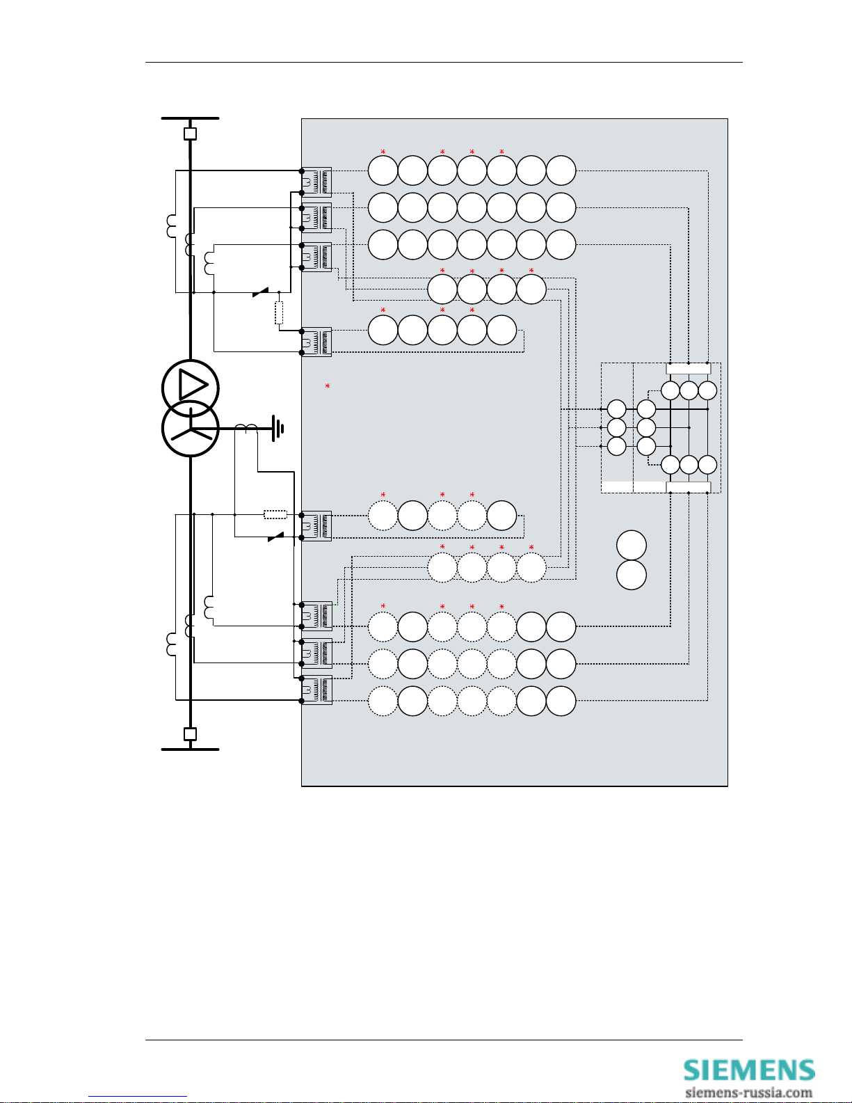
7SR242n-2aAnn-0AA0
50
BF-1
I4
50
BF-2
I4
74
CCS
(x6)
Figure 1-1 Functional Diagram: 7SR242n-2aAnn-0AA0 Relay
7SR242 Duobias Description Of Operation
©2010 Siemens Protection Devices Limited Chapter 1 Page 10 of 52
I
G1
W1-IL1(IA)
I
G2
W1-IL2(IB)
W1-I
L3(IC
)
W2-I
L3(IC
)
W2-I
L2(IB
)
W2-I
L1(IA
)
50G
(x2)
51G
(x4)
64H
81
HBL5
81
HBL5
81
HBL5
74
TCS
(x6)
7SR242n-2aAnn-0BA0
81
HBL2
81
HBL2
81
HBL2
87HS
87BD
ICT
ICT
37
(x2)
49
50
(x2)51(x2)
50
BF-1
37
(x2)
49
50
(x2)51(x2)
50
BF-1
37
(x2)
49
50
(x2)51(x2)
50
BF-1
50N
(x2)
51N
(x2)
46
BC
(x2)
37 49
37 49
37 49
50N
50
BF-2
50
BF-2
50
BF-2
46
NPS
51N
51
51
51
50
50
50
50G 51G 64H
81
HBL2
81
HBL
2
81
HBL
2
81
HBL5
81
HBL5
81
HBL5
Each function element
can be assigned to W1
or W2 CT inputs.
NOTE: The use of some
functions are mutually
exclusive
37G
(x2)
50
BF-1
I4
37G50BF-2
I4
74
CCS
(x6)
46
BC
46
NPS
(x4)
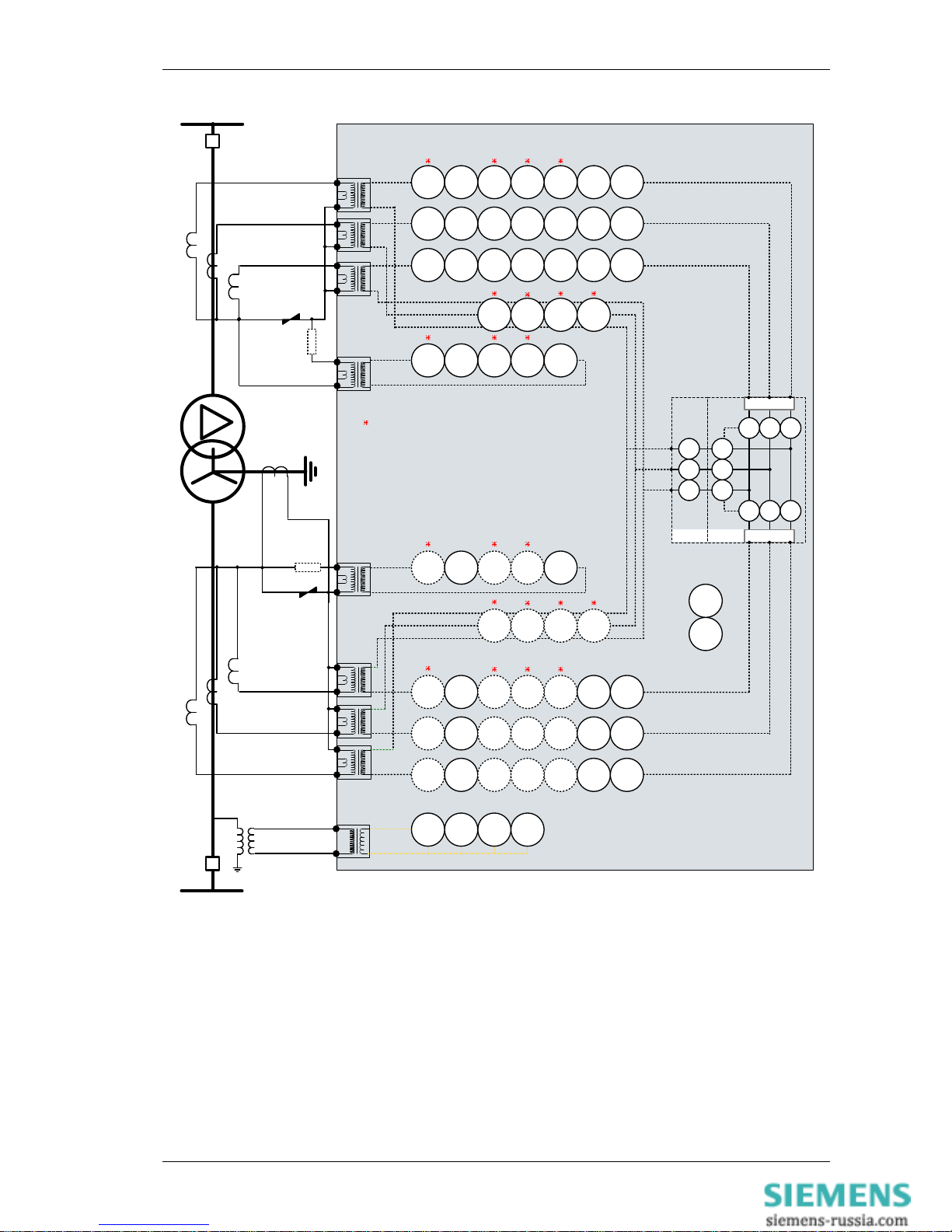
Figure 1-2 Functional Diagram: 7SR242n-2aAnn-0BA0 Relay
7SR242 Duobias Description Of Operation
©2010 Siemens Protection Devices Limited Chapter 1 Page 11 of 52
IG1
50G
(x2)
51G
(x4)
64H
W1-IL1 (IA) 81
HBL5
81
HBL5
81
HBL5
V1 (VX)
74
TCS
(x6)
59N
(x2)
27
59
(x4)
81
(x6)
IG2
W1-IL2 (IB)
W1-I
L3 (IC)
W2-I
L3 (IC)
W2-I
L2 (IB)
W2-I
L1 (IA)
7SR242n-2aAnn-0CA0
81
HBL2
81
HBL2
81
HBL2
87HS
87BD
ICT
ICT
37
(x2)
49
50
(x2)51(x2)
50
BF-1
37
(x2)
49
50
(x2)51(x2)
50
BF-1
37
(x2)
49
50
(x2)51(x2)
50
BF-1
50N
(x2)
51N
(x2)
46
BC
(x2)
37 49
37 49
37 49
50N
50
BF-2
50
BF-2
50
BF-2
46
NPS
51N
51
51
51
50
50
50
50G 51G 64H
81
HBL2
81
HBL
2
81
HBL
2
81
HBL5
81
HBL5
81
HBL5
Each function element
can be assigned to W1
or W2 CT inputs.
NOTE: The use of some
functions are mutually
exclusive
24
(x3)
37G
(x2)
50
BF-1
I4
37G50BF-2
I4
74
CCS
(x6)
46
BC
46
NPS
(x4)
Figure 1-3 Functional Diagram: 7SR242n-2aAnn-0CA0 Relay
7SR242 Duobias Description Of Operation
©2010 Siemens Protection Devices Limited Chapter 1 Page 12 of 52
BO 1
GND.
BI 1
+ve
-ve
+ve
-ve
22
24
28
2
4
BI 2
+ve
-ve
6
8
BI 3
+ve
-ve
10
12
BO 2
BO 3
BO 4
BO 5
7SR242
BI 10
+ve
-ve
2
4
BI 11
+ve
-ve
6
8
BI 12
+ve
10
BO 7
BO 8
BO 9
BI 13
+ve
12
BI 14
+ve
14
BI 15
+ve
-ve
16
18
BI 16
20
BI 17
+ve
22
BI 18
+ve
24
BI 19
+ve
-ve
26
28
+ve
BO 10
BO 11
BO 12
BO 13
BO 14
A
CT/VT
B
CT
D
Optional
I/O
1 2
27 28
1 21 2
27 2827 28
Data
Comms
(Optional)
C
D
A
Screen
B
Term.
14
16
18
20
13
14
15
16
1A
5A
1
2
3
4
1A
5A
5
6
7
8
1A
5A
9
10
11
12
1A
5A
A
IG1
V1 (VX)
27
28
17
18
19
20
5A
BI 4
+ve
18
BI 5
+ve
22
BI 6
+ve
-ve
26
28
1A
5A
1
2
3
4
1A
5A
5
6
7
8
1A
5A
9
10
11
12
B
-ve
20
-ve
24
BI 7
+ve
17
BI 8
+ve
21
BI 9
+ve
-ve
25
27
-ve
19
-ve
23
C
PSU
1 2
27 28
W1-IL1 (IA)
W1-I
L2 (IB)
W1-I
L3 (IC)
W2-I
L3 (IC)
W2-IL2 (IB)
W2-I
L1 (IA)
IG2
BO 6
Rear View
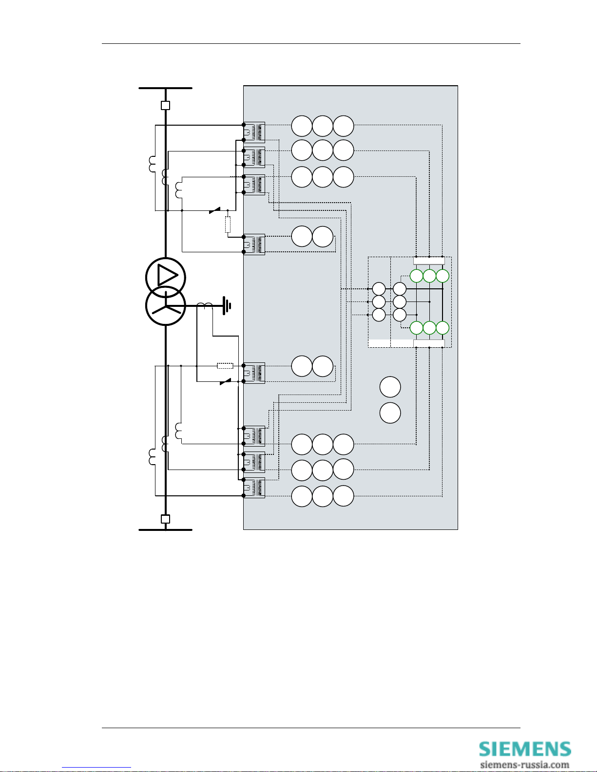
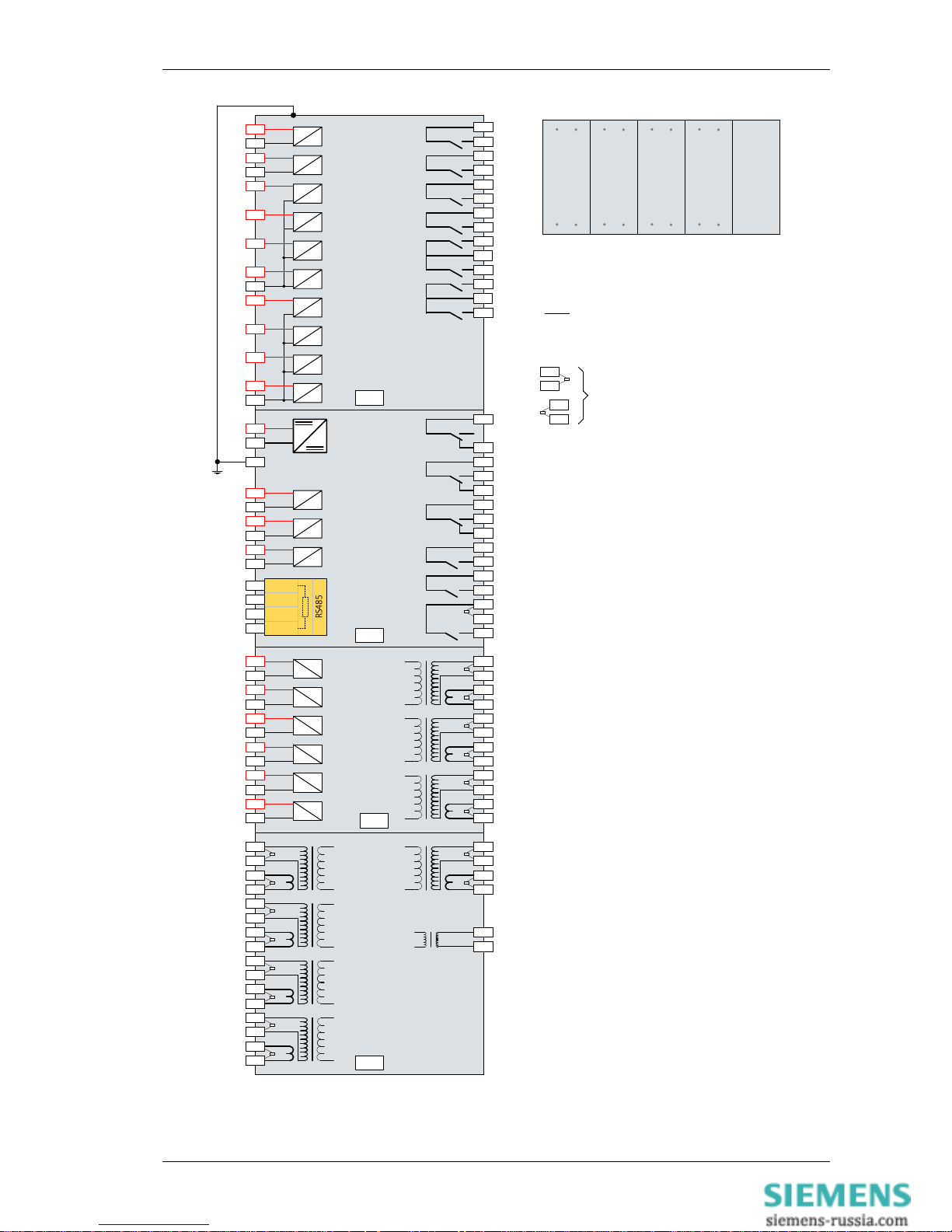
Arrangement of terminals and modules
NOTES
Shows contacts internal to relay case
assembly.
Contacts close when the relay chassis is
withdrawn from case
BI = Binary Input
BO = Binary Output
21
19
17
23
25
27
3
1
7
5
11
9
15
13
9
5
7
27
3
1
15
11
13
19
17
23
21
25
26
Figure 1-4 Connection Diagram: 7SR242 Relay

7SR242 Duobias Description Of Operation
©2010 Siemens Protection Devices Limited Chapter 1 Page 13 of 52
Section 2: Hardware Description
2.1 General
The structure of the relay is based upon the Multi-function hardware platform. The relays are supplied in either
size E8 or size E10 cases (where 1 x E = width of approx. 26mm). The hardware design provides commonality
between products and components across the Multi-function range of relays.
Table 2-1 Summary of 7SR24 Relay Configurations
Relay Current
Inputs
Voltage
Inputs
Binary
Inputs
Output
Relays
LEDs Case
7SR2422 8 1 9 6 16 E8
7SR2423 8 1 19 14 24 E10
Relays are assembled from the following modules:
1) Front Fascia with three fixed function LEDs and ordering options of configurable LEDs.
2) Processor module
3) Analogue Input module ‘A’: 3 x Current + 6 x Binary Inputs
4) Analogue Input module ‘B’: 5 x Current + 1 x Voltage.
5) Power Supply and basic Binary Input (BI) and Binary Output (BO).
6) Optional Binary Input/Output Module
7) Optional data comms module
2.2 Case
The relays are housed in cases designed to fit directly into standard panel racks. The two case options have
widths of 208mm (E8) and 260 mm (E10), both have a height of 177 mm (4U). The required panel depth (with
wiring clearance) is 242 mm. An additional 75 mm depth clearance should be allowed to accommodate the
bending radius of fibre optic data communications cables if fitted.
The complete relay assembly is withdrawable from the front of the case. Contacts in the case ensure that the CT
circuits remain short-circuited when the relay is removed.
The rear terminal blocks comprise M4 female terminals for wire connections. Each terminal can accept two 4mm
crimps.
Located at the top rear of the case is a screw clamp earthing point, this must be connected to the main panel
earth.
2.3 Front Cover
With the transparent front cover in place the user only has access to the ▼ and TEST/RESET► buttons,
allowing all areas of the menu system to be viewed, but preventing setting changes and control actions. The only
‘action’ that is permitted is to reset the Fault Data display, latched binary outputs and LEDs by using the
TEST/RESET button.
The front cover is used to secure the relay assembly in the case.
7SR242 Duobias Description Of Operation
©2010 Siemens Protection Devices Limited Chapter 1 Page 14 of 52
2.4 Power Supply Unit (PSU)
The relay PSU can be directly connected to any substation dc system rated from 30V dc to 220V dc.
In the event of the station battery voltage level falling below the relay minimum operate level the PSU will
automatically switch itself off and latch out – this prevents any PSU overload conditions occurring. The PSU is
reset by switching the auxiliary supply off then on.
2.5 Operator Interface/ Fascia
The operator interface is designed to provide a user-friendly method of controlling, entering settings and retrieving
data from the relay.
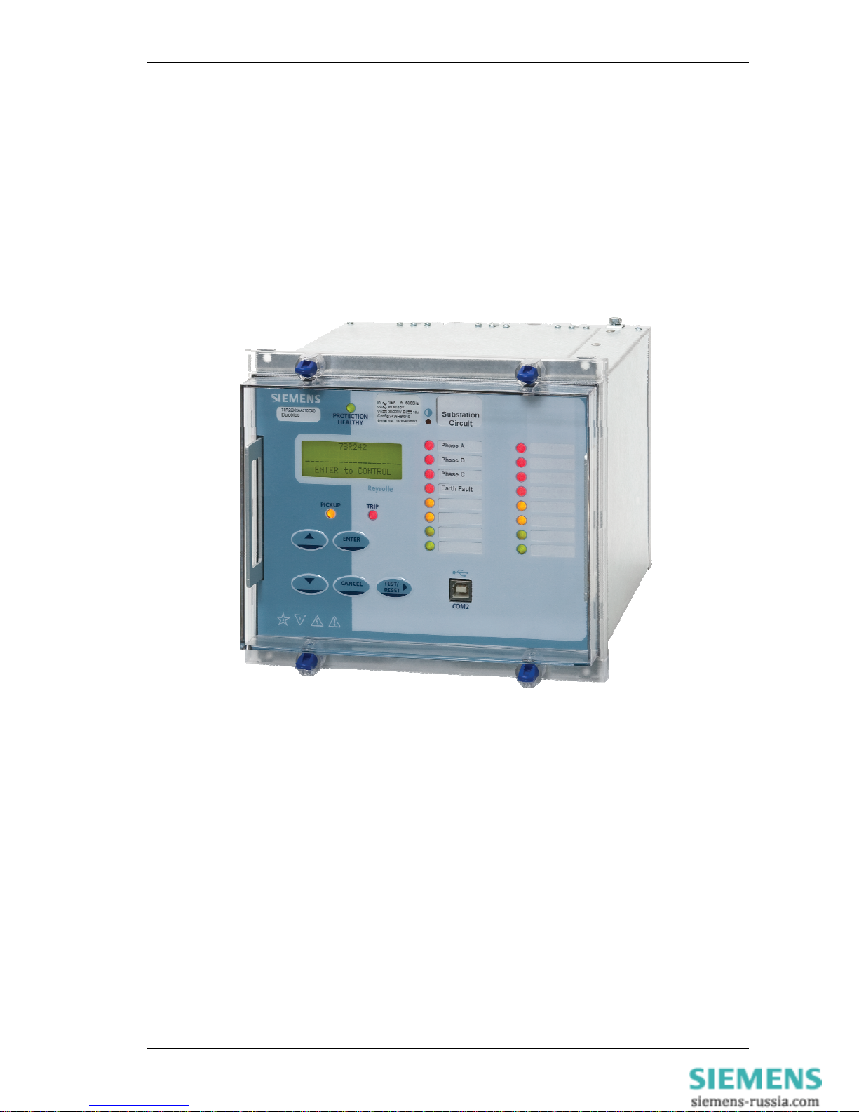
Figure 2-1 7SR24 with 3 + 16 LEDs in E8 Case
NOTE: Pushbuttons on cover not shown
The fascia is an integral part of the relay. Handles are located at each side of the element to allow it to be
withdrawn from the relay case.
Relay Information
Above the LCD three labels are provided, these provide the following information:
1) Product name and order code.
2) Nominal current rating, rated frequency, voltage rating, auxiliary dc supply rating, binary input supply
rating, configuration and serial number.
3) Blank label for user defined information.
A ‘template’ is available within the ‘Reydisp’ program to allow users to create and print customised LED label
inserts.
7SR242 Duobias Description Of Operation
©2010 Siemens Protection Devices Limited Chapter 1 Page 15 of 52
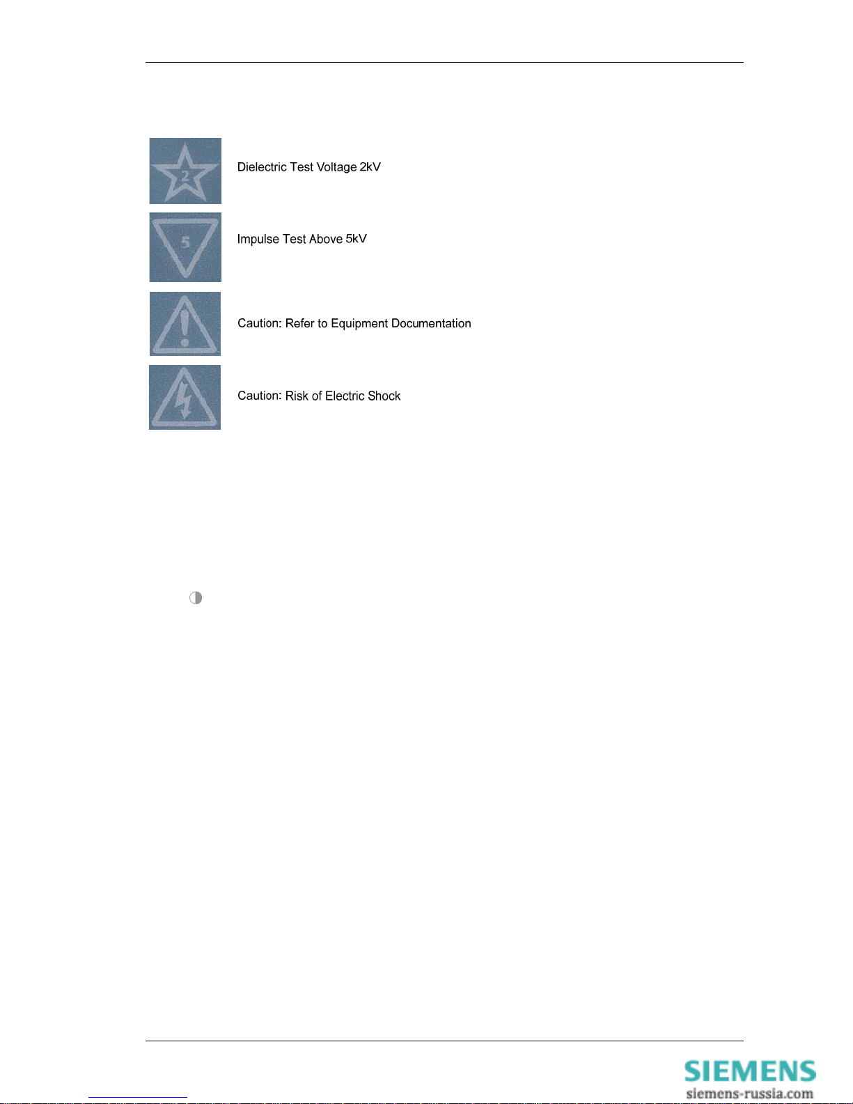
The warning and information labels on the relay fascia provide the following information:
Liquid Crystal Display (LCD)
A 4 line by 20-character liquid crystal display indicates settings, instrumentation, fault data and control
commands.
To conserve power the display backlighting is extinguished when no buttons are pressed for a user defined
period. A setting within the “SYSTEM CONFIG” menu allows the timeout to be adjusted from 1 to 60 minutes and
“Off” (backlight permanently on). After an hour the display is completely de-activated. Pressing any key will reactivate the display.
The LCD contrast can be adjusted using a flat blade screwdriver to turn the screw located below the contrast
symbol
. Turning the screw clockwise increases the contrast, anti-clockwise reduces the contrast.
‘PROTECTION HEALTHY’ LED
This green LED is steadily illuminated to indicate that DC voltage has been applied to the relay power supply and
that the relay is operating correctly. If the internal relay watchdog detects an internal fault then this LED will
continuously flash.
‘PICKUP’ LED
This yellow LED is illuminated to indicate that a user selectable function(s) has picked up. The LED will self reset
after the initiating condition has been removed.
Functions are assigned to the PICKUP LED in the OUTPUT CONFIG>PICKUP CONFIG menu.
‘TRIP’ LED
This red LED is steadily illuminated to indicate that a user selectable function has operated to trip the circuit
breaker. Functions are assigned to the ‘Trip’ LED using the OUTPUT CONFIG>Trip Contacts setting.
Operation of the LED is latched and can be reset by either pressing the TEST/RESET► button, energising a
suitably programmed binary input, or, by sending an appropriate command over the data communications
channel(s).
Indication LEDs
Relays have either 8 or 16 user programmable LED indicators. Each LED can be programmed to be illuminated
as either green, yellow or red. Where an LED is programmed to be lit both red and green it will illuminate yellow. .
Each LED can be assigned two different colours dependent upon whether a Start/Pickup or Operate condition

7SR242 Duobias Description Of Operation
©2010 Siemens Protection Devices Limited Chapter 1 Page 16 of 52
initiates operation. The LED illumination colour is assigned in the OUTPUT CONFIG>LED CONFIG menu for both
Pickup and Operate initiation.
Functions are assigned to the LEDs in the OUTPUT CONFIG>OUTPUT MATRIX menu.
Each LED can be labelled by withdrawing the relay and inserting a label strip into the pocket behind the front
fascia. A ‘template’ is available to allow users to create and print customised legends.
Each LED can be user programmed as hand or self–resetting. Hand reset LEDs can be reset by either pressing
the TEST/RESET► button, energising a suitably programmed binary input, or, by sending an appropriate
command over the data communications channel(s).
The status of hand reset LEDs is maintained by a back up storage capacitor in the event of an interruption to the
d.c. supply voltage.
Standard Keys
The relay is supplied as standard with five pushbuttons. The buttons are used to navigate the menu structure and
control relay functions. They are labelled:
▲ Increases a setting or moves up menu.
▼ Decreases a setting or moves down menu.
TEST/RESET► Moves right, can be used to reset selected functionality and for LED test (at
relay identifier screen).
ENTER Used to initiate and accept settings changes.
CANCEL. Used to cancel settings changes and/or move up the menu structure by one
level per press.
NOTE: All settings and configuration of LEDs, BI, BO and function keys can be accessed and set by the user
using these keys. Alternatively configuration/settings files can be loaded into the relay using ‘ReyDisp’.
2.6 Current Inputs
In total eight current inputs are provided on the Analogue Input modules. Terminals are available for both 1A and
5A inputs. CT ratios are input by the user in the CT/VT CONFIG menu.
Current is sampled at 1600Hz for 50Hz systems and 1920Hz for 60Hz systems (32 samples per cycle).
The waveform recorder samples and displays current input waveforms at 32 samples per cycle.
2.7 Voltage Input
An optional voltage input is provided on the Analogue Input module ‘A’.
VT ratios are input by the user in the CT/VT CONFIG menu.
Voltage is sampled at 1600Hz for 50Hz systems and 1920Hz for 60Hz systems (32 samples per cycle).
The waveform recorder displays the voltage input waveform at 32 samples per cycle.
 Loading...