

Page 1

PRO-106
Digital Trunking Hand Held Scanner
Catalog Number: 20-106
CONTENTS
20-106
Page
Specifications .................................................................................................................................................... 2
Block Diagram ................................................................................................................................................... 4
Alignment and Adjustment ................................................................................................................................ 5
Troubleshooting ............................................................................................................................................... 10
Printed Circuit Board ....................................................................................................................................... 15
Wiring Diagram ................................................................................................................................................ 19
Exploded View ................................................................................................................................................. 20
Mechanical Parts List....................................................................................................................................... 21
Electrical Parts List .......................................................................................................................................... 22
Semiconductor Lead Identification ................................................................................................................. 65
Microprocessor (IC306) Port Format............................................................................................................... 71
Schematic Diagram ......................................................................................................................................... 72
© 2008 RadioShack Corporation
RadioShack is a registered trademark used by RadioShack Corporation.
All Rights Reserved.
Page 2

SPECIFICATIONS
Frequency Coverage 25.000-26.960 MHz 10 kHz steps (AM)
26.965-27.405 MHz 10 kHz steps (AM)
27.410-29.505 MHz 5 kHz steps (AM)
29.510-29.700 MHz 5 kHz steps (FM)
29.710-49.830 MHz 10 kHz steps (FM)
49.835-54.000 MHz 5 kHz steps (FM)
108.000-136.99166 MHz 8.33 kHz steps (AM)
137.000-137.995 MHz 5 kHz steps (FM)
138.000-143.9875 MHz 12.5 kHz steps (FM)
144.000-147.995 MHz 5 kHz steps (FM)
148.000-150.7875 MHz 12.5 kHz steps (FM)
150.800-150.845 MHz 5 kHz steps (FM)
150.8525-154.4975 MHz 7.5 kHz steps (FM)
154.515-154.640 MHz 5 kHz steps (FM)
154.650-156.255 MHz 7.5 kHz steps (FM)
156.275-157.450 MHz 25 kHz steps (FM)
157.470-161.5725 MHz 7.5 kHz steps (FM)
161.600-161.975 MHz 5 kHz steps (FM)
162.000-174.000 MHz 12.5 kHz steps (FM)
216.0025-219.9975 MHz 5 kHz steps (FM)
220.000-224.995 MHz 5 kHz steps (FM)
225.000-379.99375 MHz 6.25 kHz steps (AM)
380.000-419.9875 MHz 12.5 kHz steps (FM)
420.000-450.000 MHz 5 kHz steps (FM)
450.00625-469.99375 MHz 6.25 kHz steps (FM)
470.000-512.000 MHz 12.5 kHz steps (FM)
764.000-805.996875 MHz 3.125 kHz steps (FM)
806.000-823.9875 MHz 12.5 kHz steps (FM)
849.000-868.9875 MHz 12.5 kHz steps (FM)
894.000-939.9875 MHz 12.5 kHz steps (FM)
940.000-960.000 MHz 6.25 kHz steps (FM)
1240.000-1300.000 MHz 6.25 kHz steps (FM)
Unit Nominal Limit
Signal to noise ratio (FM and AM)
RF input: 100 μV 25-54 MHz dB 40 30
Dev. 3 kHz at 1 kHz 108-136.99166 MHz dB 40 30
Mod.: 60% at 1 kHz 137-174 MHz dB 40 30
216.0025-299.99375 MHz dB 40 30
300-512 MHz dB 35 25
764-960 MHz dB 35 25
1240-1300 MHz dB 35 25
Squelch sensitivity
at threshold (AM/FM) μV 0.5 2
at tight (FM) dB 25 15
at tight (AM) dB 20 10
Data decode sensitivity
WX Alert 1050 Hz tone 3 kHz Dev. at 162.4 MHz μV 0.3 1
2
Page 3

Unit Nominal Limit
Spectrum sweeper sensitivity at 450 MHz dBm -60 -50
Sensitivity
FM: (S+N)/N=20 dB 25-54 MHz μV 0.3 1
Dev.: 3 kHz at 1 kHz 108-136.99166 MHz μV 0.3 1
137-174 MHz μV 0.5 2
216.0025-224.995 MHz μV 0.5 2
225-299.99375 MHz μV 0.5 2
300-405.9875 MHz μV 0.8 3
406-512 MHz μV 0.5 2
764-960 MHz μV 0.7 3
1240-1300 MHz μV 0.7 4
AM: (S+N)/N=20 dB 25-54 MHz μV13
Mod.: 60% at 1 kHz 108-136.99166 MHz μV13
137-174 MHz μV 1.5 5
216.0025-224.995 MHz μV 1.5 5
225-299.99375 MHz μV26
300-405.9875 MHz μV310
406-512 MHz μV26
764-960 MHz μV26
1240-1300 MHz μV312
Selectivity AM 25-27.995 MHz -6 dB kHz ±4 >±2.5
-50 dB kHz ±6 <±12
Other frequency -6 dB kHz ±7 >±4.5
-50 dB kHz ±13 <±18
Spurious rejection (Except Primary image) at 154.1 MHz dB 40 30
Acceptable radio frequency displacement (EIA RS-204D) kHz ±6 ±3
Residual noise Volume control, set to its minimum, squelched mV 1 3
Scanning rate without trunking channels/sec. 55 45-66
Search rate at 162.25-167.25 MHz steps/sec. 90 80-100
Scan delay time sec. 2 1-3
Audio output power 10% THD mW 170 140
Current drain (using AC or DC adapter) Squelched mA 140 170
Working memory 1,800 programmed object using flexible scannable object system
Display Liquid crystal display (16-charactor x 4-line, plus icon)
Receiving system Triple conversion PLL super-heterodyne,
1st IF: 380.8 MHz/2nd IF: 21.4 MHz/3rd IF: 455 kHz
Power source 6V DC negative ground only
4AA batteries or a suitable adapter
Jacks Antenna, earphone, PC/IF, and external power
Dimensions (HWD) 5 3/4 x 2 9/16 x 1 5/8 inches (145 x 65 x 42 mm)
Weight apporox. 8.5 oz. (240 g) without antenna and batteries
Note: Nominal specs represent the design specs. All units should be able to approximate these specifications.
Some units will exceed while some may drop below these specs. Limit specs represent the absolute worst condition
still considered acceptable. A unit should NEVER fail to meet limit specs.
3
Page 4
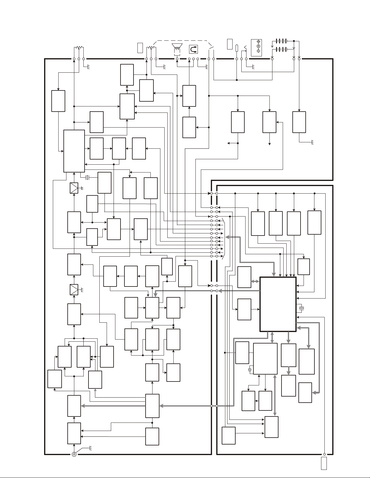
BLOCK DIAGRAM
x4
Batt
SQ
IC6a
Noise Amp
VR6b
IC8b
Buffer Amp
VOL
IC8a
Pre Amp
AM/FM
Switching
IC9a,9b,10a,10d
VR6a
Speaker
Mute
IC10b,Q32
J2
IC12
Audio Amp
IC11
Voltage
Regulator
PWR
J3
Power SW
Voltage
DC 9V
Batt
AAx4
IC13
Regulator
IC14
Regulator
Switching
Ni-cd
Charger
Q33,34,35,36
CF1
Filter
IC7
Ceramic
3rd Local Mixer
Quadrature Detector
3rd IF Amp Noise Amp
XF 2
2nd IF
21.4MHz
XF 1
1st IF
X2
Q10
2nd IF Amp
2nd
Local
Q9
2nd Mix
1st
Local
IC2
1st Mix
Swithing
3rd Local
20.945MHz
Q13,Q17
Switching
Q14,D23
Switching
CF2
Filter
Ceramic
455kHz
IC9c,9d
Q15,Q16
2nd IF Amp
Q30
Amp
Buffer
X 1
12.75MHz
Q31
Filter
Switching
Q11
AGC Amp
Q29
VCO3
IC4
TC XO
Q12
Switching
3r
Detector,
D27,28,IC3
Comparator
Q18,Q19
Switching
Filter
Q27,Q28
Low-Pass
IC4
PLL
DC-DC
Converter
Filter
Q25,Q26
Low-Pass
ce
Voi
3.3V
d
L
o
ca
l
t.
C
o
n
Keytone
Mute
/AM/DigitalFM
Filter SW
ont.
Scan C
SQ IN
Search Cont.
LD
IC5
Power
SW
Data
PLL
a Dat
2 SQ
3.3V
Data Filter
Low Speed
IC304,305b
IC301
Memory
IC303
Voltage
Detector
Power Save Cont.
B+ (3.3V)
Filter
Filter
IC306a,b
WX Alert Data
HiSpeed Data
CPU
IC307
Filter
IC305a
IC306c,d
SAME Data
Q304
Reset
Zeromatic
X301
11.0592MHz
Q24
Amp
Buffer
Q3,Q4
RF Amp
Q2
Switching
25-54MHz
108-225MHz
225-406MHz
406-512MHz
764-1300MHz
Q7
RF Amp
BPF
D1,D2
Attenuator
J1
ANT
Q8
AGC Amp
Q5,Q6
Switching
Q20
VCO1
Q21
Switching
IC1
Att. Control
Band Select
Q1
Switching
Q22
VCO2
IC308
Voltage
Regulator
Q23
Switching
Cont.Data
X302
Flash
IC309
Voltage
Regulator
4
DSP
IC310
18.432MHz
Shift
IC312
IC311
Memory
Resister
CODEC
Q301,302
LED Driver
303,305,306
Keyboard
LED
LCD
IC313
J301
PC/IF
Page 5
ALIGNMENT AND ADJUSTMENT
ALIGNMENT AND TEST POINT
TP3 TP6 TP5 TP4
VR3
VR4
L23
ALIGNMENT PREPARATION
Test Equipment Required
z Oscilloscope
z DC SSVM
z FM signal generator
z Frequency counter (800 MHz)
Notes:
L26
L24
TP1 TP2
VR5
VR2
Linear PCB
T4
z Use non-metallic tuning tools.
z The test equipment and receiver should be warmed up for at least 10 minutes before proceeding with alignment.
z The signal level from the generator should be kept as low as possible to obtain a usable output.
z To tune the frequency, press TUNE, frequency number including decimal point, then press ENT.
If you make a mistake, press CL to delete a single digit or hold CL about 2 seconds to start over.
5
Page 6
ALIGNMENT PROCEDURES
PLL2 VCO Alignment
gnitteSlortnoCnoitcennoCtnemurtsnItseTtsujdAtluseR
.NO:lortnocEMULOV/FFO
ylluF:lortnocHCLEUQS
lcretnuoc
.zHM215otenuT
.)WCC(esiwkco
PLL1 VCO1 Alignment
gnitteSlortnoCnoitcennoCtnemurtsnItseTtsujdAtluseR
.NO:lortnocEMULOV/FFO
.WCC:lortnocHCLEUQS
enuT
.zHM
467dnazHM069ot
PLL1 VCO2 Alignment
gnitteSlortnoCnoitcennoCtnemurtsnItseTtsujdAtluseR
.NO:lortnocEMULOV/FFO
.WCC:lortnocHCLEUQS
uT
.zHM5200.012
dnazHM0031oten
.3PTotMVSSCDtcennoC
.1erugiFeeS
.2PTotMVSSCDtcennoC
.2erugiFeeS
.2PTotMVSSCDtcennoC
.2erugiFeeS
62LCDehtnostlov0.2ot62LtsujdA
.2dna1selbaTeeS.MVSS
32LtsujdadnazHM069otenuT.1
.MVSSCDehtnostlov0.81ot32L
erusebdnazHM467otenuT.2
.stlov0.4-0.2sdaerMVSSCDeht
rofyrassecenerastnemtsujdaoN(
.1elbaTeeS).lioceht
42LtsujdadnazHM0031otenuT.1
.MVSSCDehtnostlov0.02ot42L
ebdnazHM5200.012otenuT.2
0.5-0.2sdaerMVSSCDehterus
erastnemtsujdaoN(.stlov
elbaTeeS).liocehtrofyrassecen
.1
5200.6122PTtastlov0.5-0.2
Under Test
ycneuqerFegatloV
zHM000.0692PTtastlov0.91-0.71
zHM000.4672PTtastlov0.4-0.2
zHM000.00312PTtastlov0.12-0.91
zHM
zHM000.2153PTtastlov2.2-8.1
TP3Unit
Figure 1
DC SSVM
Table 1
DC SSVM
TP2Unit
Under Test
Figure 2
6
Page 7
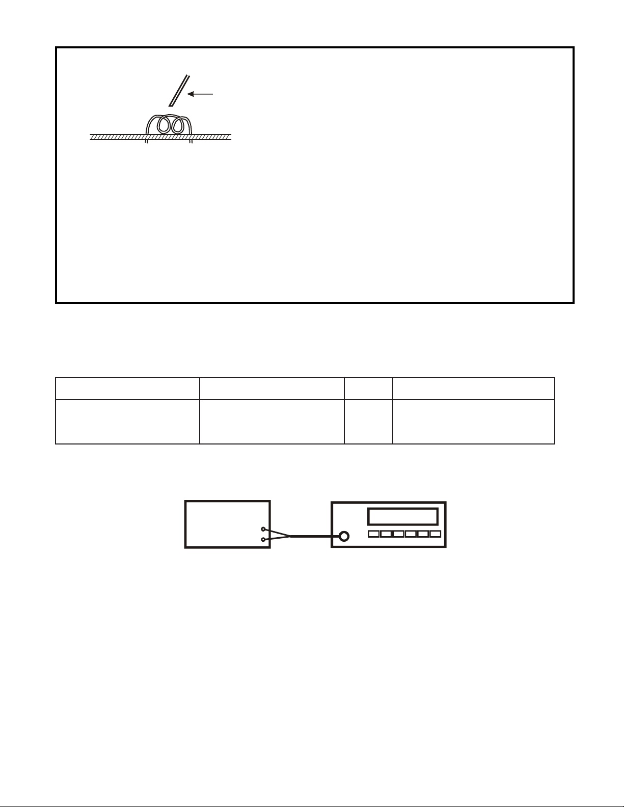
Adjustment of Coils L23, L24, and L26
Use
non-metallic
Coil
tuning tool
Each coil should be adjusted carefully by changing
the pitch of the coil little by little using a non-metallic
tuning tool as shown in Figure 3.
PCB
Notes:
z Be very careful when doing coil pitch adjustment
because it greatly affects the frequency.
z Secure the coil with glue after alignment. Be sure
the glue is dry and the coil is secured. Also, be
sure that the environmental temperature is nor-
mal. Then, repeat VCO (PLL2 and PLL1) align-
ments on Page 6.
Figure 3
Table 2
Increase the pitch of the coil when the measured volt-
age at TP2 or TP3 is higher than the voltage listed in
Table 2 for the PLL2 VCO alignment, PLL1 VCO1 align-
ment, and PLL1 VCO2 alignment.
Decrease the pitch of the coil when the measured volt-
age at TP2 or TP3 is lower than the voltage listed in
Table 2 for the PLL2 VCO alignment, PLL1 VCO1 align-
ment, and PLL1 VCO2 alignment.
Reference Frequency Osc. Confirmation
gnitteSlortnoCnoitcennoCtnemurtsnItseTtsujdAnoitamrifnoC
.NO:lortnocEMULOV/FFO
.WCC:lortnocHCLEUQS
tenuT
.zHM471o
.1PTotretnuoc
.4erugiFeeS
ycneuqerfehttcennoC
---retnuocycneuqerfehtmrifnoC
.zHk1-/+zHM577.455sdaer
Note: Care should be taken not to make any contact between TP1 and the shield case.
Frequency Counter
Unit
Under Test
TP1
Figure 4
7
Page 8

455 kHz FM Discriminator Coil Alignment
gnitteSlortnoC
.NO:lortnocEMULOV/FFO
.WCC:lortnocHCLEUQS
068,zHM471otenuT
.zHM054dna,zHM
FM Signal
Generator
3rd Local Alignment
gnitteSlortnoC
.4PTotMVSS
.5erugiFeeS
tnemurtsnItseT
noitcennoC
langisehttcennoC
CDehtdnakcaj
ANT. Jack
TNAehtotrotareneg
Unit
Under Test
noitcennoC
tsujdAtluseR
4Trotareneglangise
.MVSS
TP4
Figure 5
tnemurtsnItseT
tsujdAtluseR
htteS.zHM471otenuT.1
).domon(tuptuoVu001,zHM471otycneuqerf
CDehtnostlov50.0-/+3.1rof4Ttsujdadna
DC SSVM
.NO:lortnocEMULOV/FFO
.WCC:lortnocHCLEUQS
6.451otenuT
,5214.371,05
.zHM5200.612dna
FM Singal Generator
langisehttcennoC
otretnuocycneuqerfdna
.6erugiFeeS.5PT
ANT
Unit
Under Test
2R
V
kcajTNAehtotrotareneg
3RV
4RV
k554siycneuqerfehtos
ycnequerfrotareneglangisehtteS.1
.)noitaludomoN(zHM056.451ot
4RVtsujdadnazHM056.451otenuT
01-/+zH
.zH
ycneueqerfrotareneglangisehtteS.2
.)noitaludomoN(zHM5214.371ot
371otenuT
tsujdadnazHM5214.
-/+zHk554siycneuqerfehtos2RV
.zH01
ycneuqerfrotareneglangisehtteS.3
t
.)noitaludomoN(zHM5200.612o
tsujdadnazHM5200.612otenuTS
-/+zHk554siycneuqerfehtos3RV
.zH01
Frequency Counter
TP5
Figure 6
8
Page 9

IF (380.8 MHz) Trap Adjustment
gnitteSlortnoCnoitcennoCtnemurtsnItseTtsujdAtluseR
.zHM604otenuT
FM Signal
Generator
.NO:lortnocEMULOV/FFO
.WCC:lortnocHCLEUQS
ANT. Jack
dnakcajTNAehtot
.7erugiFeeS.daol
Unit
Under Test
r
otareneglangisehttcennoC
enohpdaehotepocsollicso
ymmudmho-8ssorcakcaj
Headphone
Jack
Figure 7
81LrotareneglangisehtteS.1
t
es
3:MF,zHM057.083otycneuqerf
.zHk1tanoitaivedzHk
ehtesaercedot81LtsujdA.2
.ytivitisn
rotareneglangisehtteS.3
3:MF,zHM000.604otycneuqerf
kcehcdnazHk1tanoitaivedzHk
ehtseviecerrennacsehttah
.langis
Oscilloscope
8ohm
Signal Meter Alignment
gnitteSlortnoCnoitcennoCtnemurtsnItseTtsujdAtluseR
.NO:lortnocEMULOV/FFO
.WCC:lortnocHCLEUQS
nuT
.zHM001.451ote
FM Signal
Generator
.5PTotMVSS
.8erugiFeeS
ANT. Jack
rotareneglangisehttcennoC
CDehtdnakcajTNAehtot
Unit
Under Test
Figure 8
TP6
5RVrotareneglangisehtteS
1.451otycneuqerf
.MVSSCDehtno
DC SSVM
69-,zHM00
dna)noitaludomon(tuptuomBd
stlov52.0-/+522.2rof5RVtsujda
9
Page 10
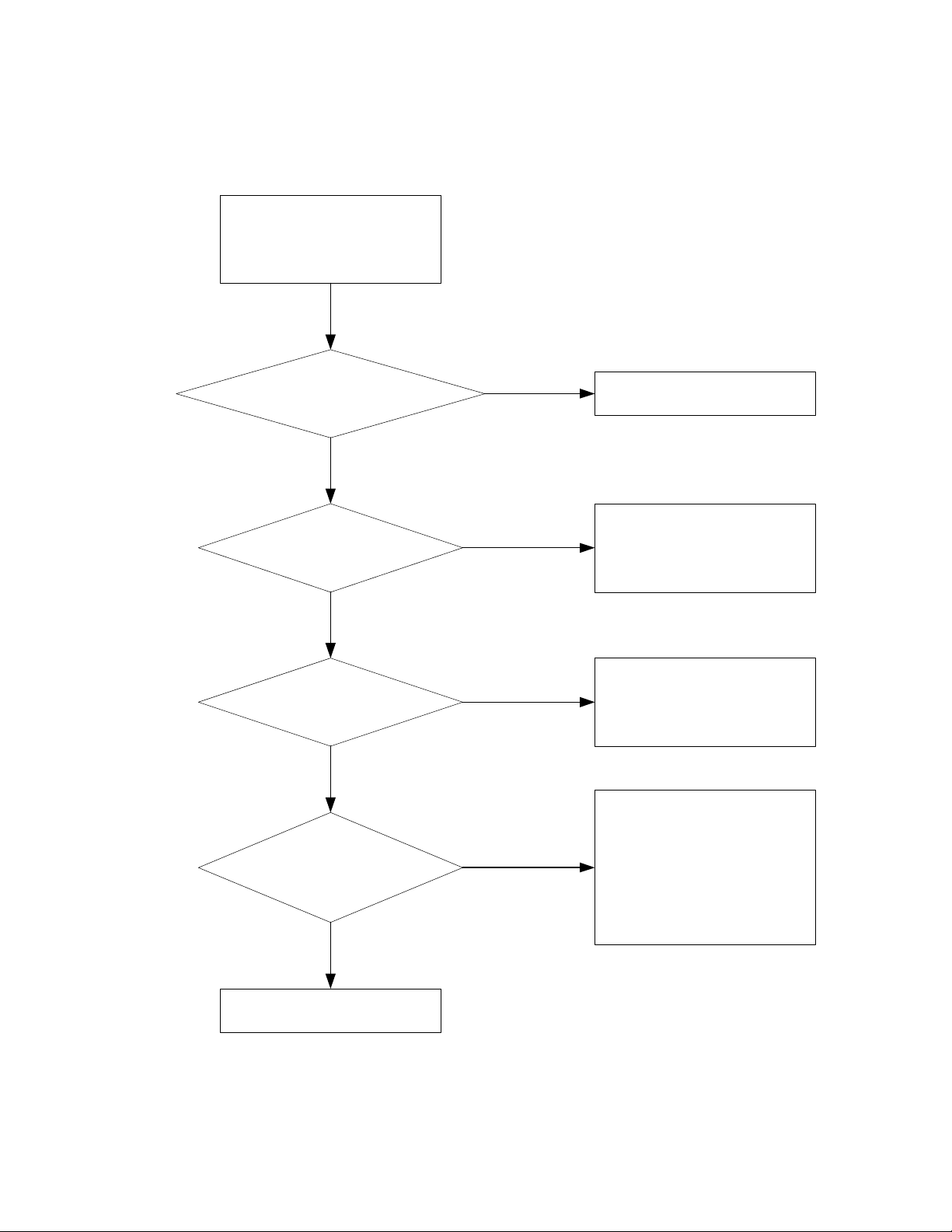
Reception Check
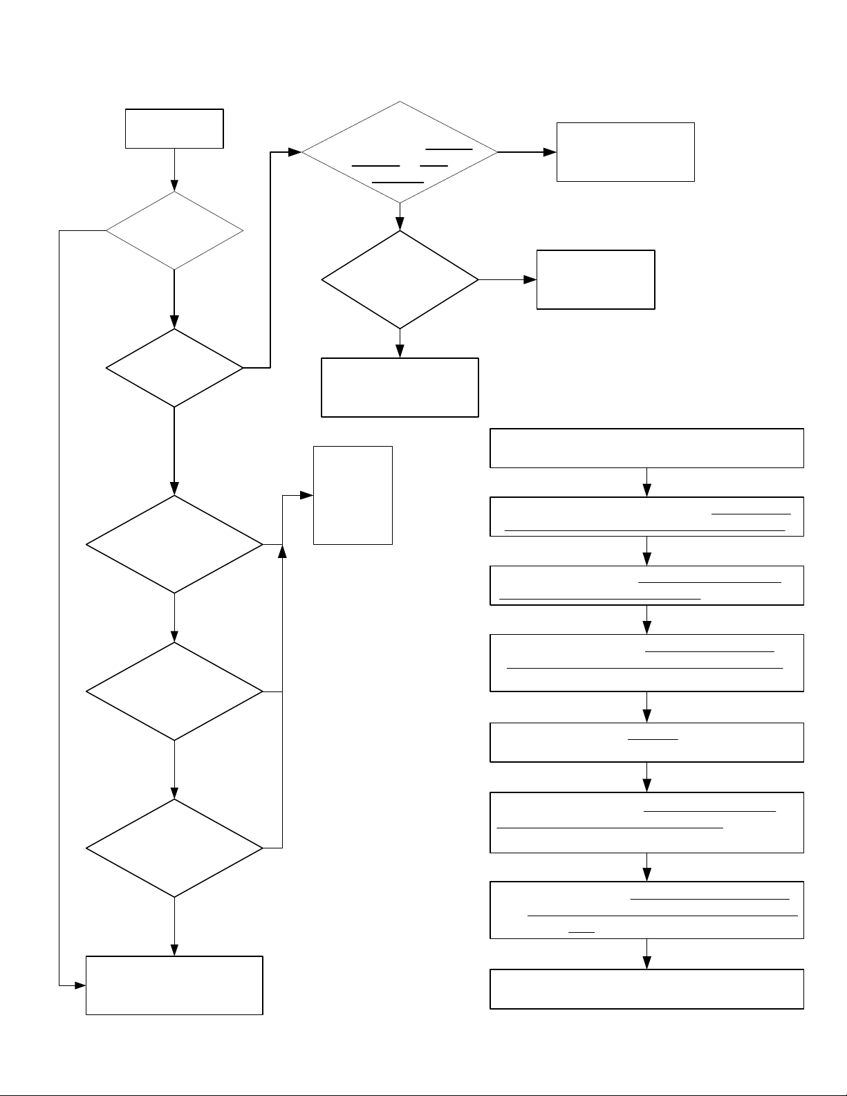
TROUBLESHOOTING
Power ON
NO
Does the
display work
properly?
Is the display
normal?
Is the voltage
of TP2 about 18 V at
960 MHz?
YES
YES
YES
NO
NO
Does display
freeze showing Waiting
for DSP or DSP
Loder ....
NO
Is EEPROM check
program OK?
YES
Defective IC307, LCD
and/or associated
circuit.
Defective
PLL circuit
(IC4) or
VCO
circuit.
Proceed to DSP
section (Boot
YES
NO
Press 0 while the scanner shows -Welcom To-
Object Oriented Digital Trunking RadioShack.
The scanner shows System Tests: Select a
Test... Exits if no key is pressed. Then press 5.
section) check.
Defective IC301.
EEPROM check program
procedure as follows:
Power on the scanner.
Is the voltage
of TP2 about 20 V at
1300 MHz?
YES
Is the voltage
of TP3 about 2.0 V at
512 MHz?
YES
Proceed to Microprocessor
check.
NO
NO
The scanner shows EEPROM Test Erase
Momory ENTER if APPROVE CLEAR to EXIT.
Then press ENT.
The scanner shows Testing, and automatically
starts the EEPROM test program.
The scanner shows GLOB EEPROM area
initialized to defaults. Press any key. Then press
any key.
The scanner shows Initializing the File system
then File system initialized to defaults. Press any
key. Then press any key.
The scanner initializes the working memory.
Note: This procedure clears all information you
stored in the scanner's working memory.
10
Page 11
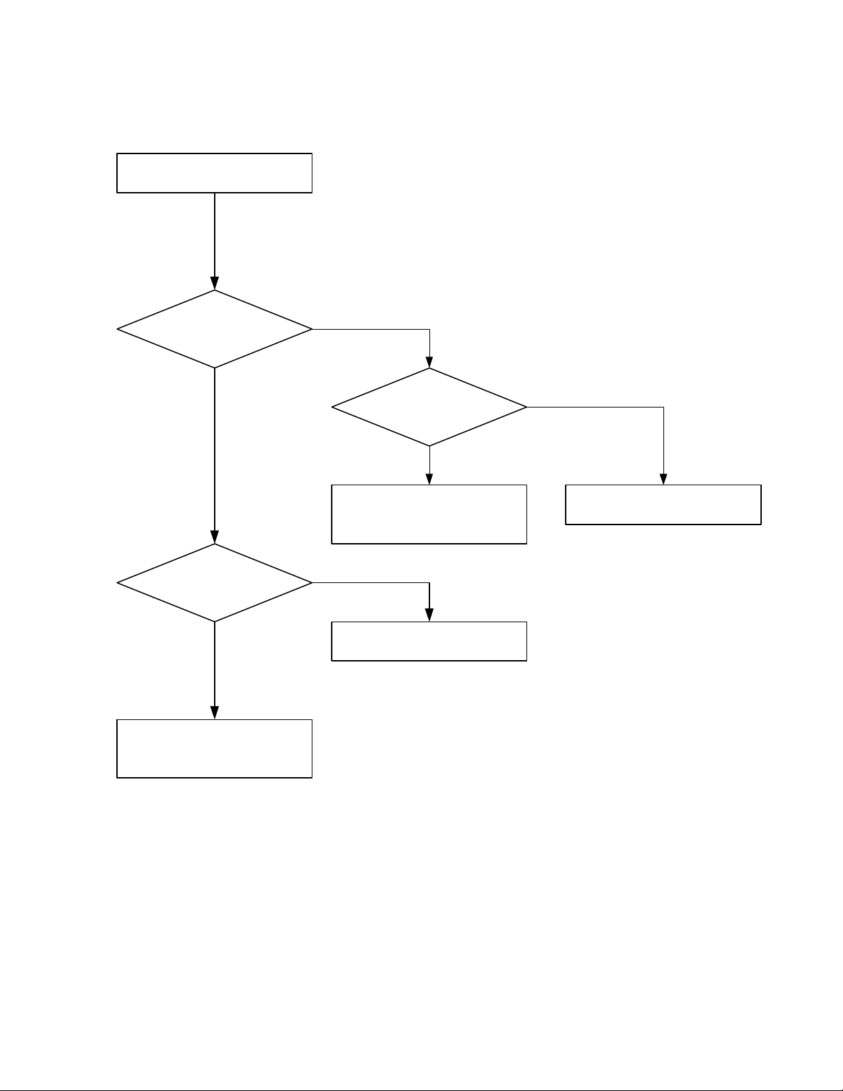
Audio Section
No audio
Is
there any audio at pin 6
of IC12?
YES
Does
5 V exist at IC12
pin 7?
YES
NO
Is
there any audio at
IC8 Pin 1?
YES
Defective IC10, Q32 and/or
associated circuit.
NO
Defective IC11 and/or R167.
NO
Defective IC8, IC10 and/or
associated circuits.
Defective IC12 and/or
associated circuit.
11
Page 12
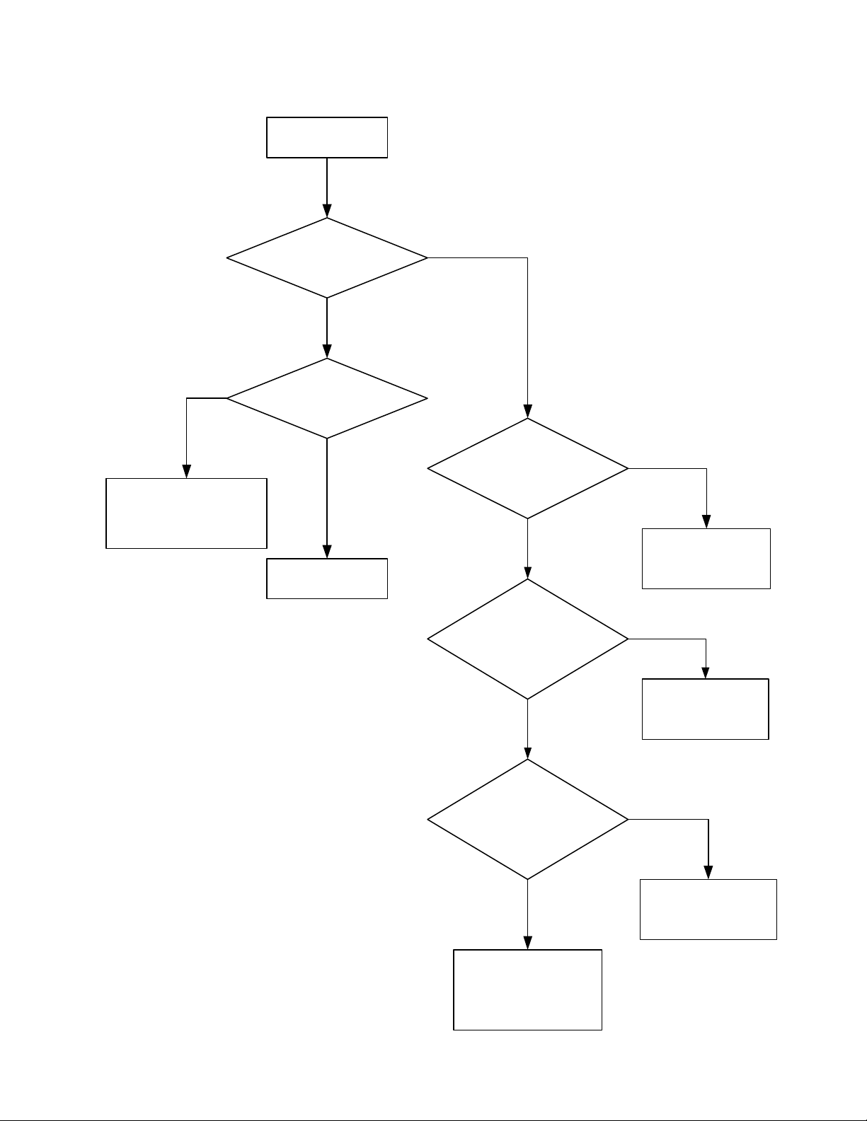
Microprocessor Check
Power ON.
NO
Defective key contact or
CPU Pin 47-52, Pin 55-
59, Pin 61.
Does the display
work properly?
YES
Does the key entry
work properly?
YES
IC307 is OK.
NO
Does
3.3 volts exist at IC307
pin 14 and 60?
YES
Does 3.3 volts exist
at IC307 pin 17.
NO
Defective IC13
and/or associated
circuit.
NO
YES
Is the clock
oscillation normal at pin
11 of IC307?
YES
Defective IC307, LCD
and/or associated
circuit.
12
Defective IC303
and/or associated
circuits.
NO
Defective X301 and/
or associated
circuits of IC307.
Page 13
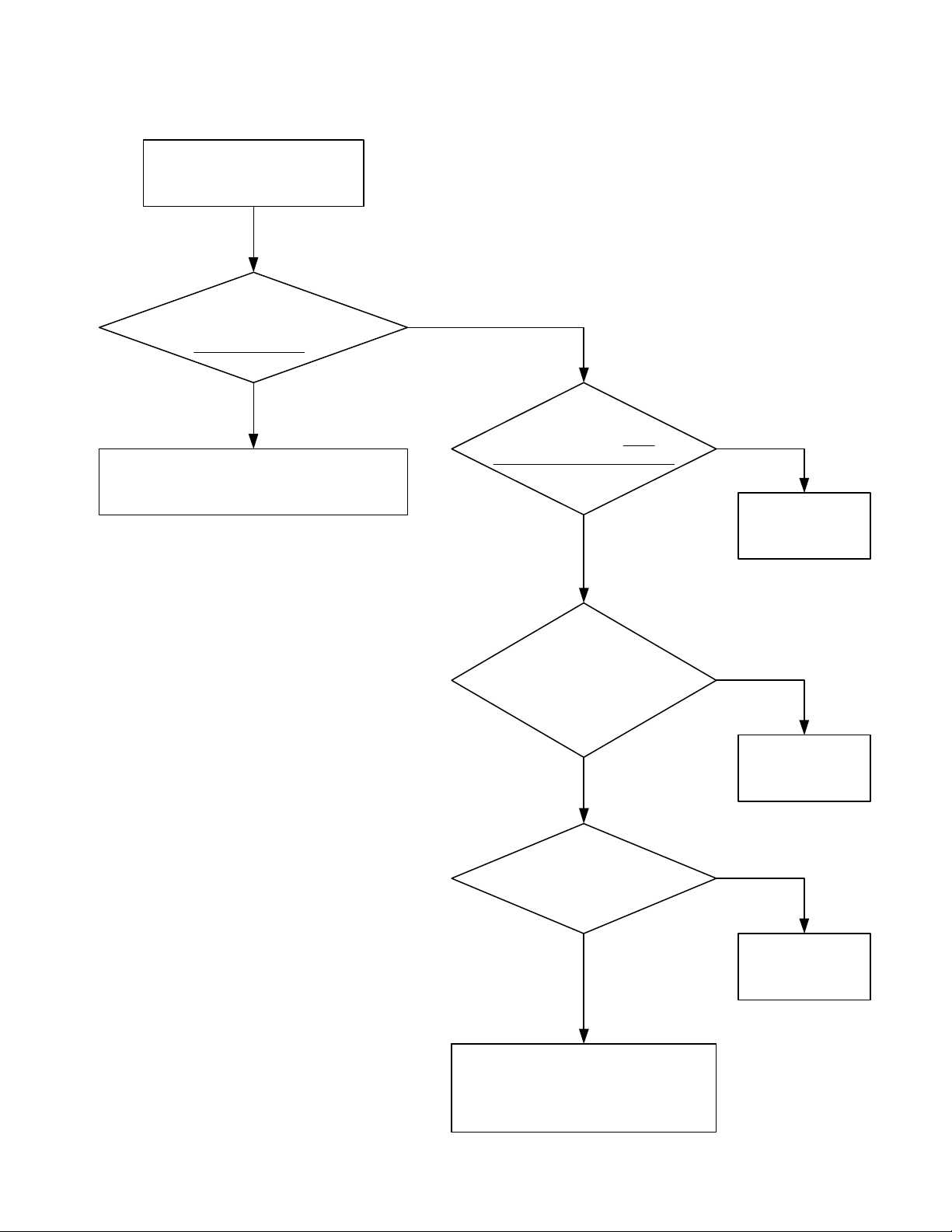
DSP Section (Boot Section)
Power ON
Does the
scanner's display freeze showing
Waiting for DSP?
YES
Defective IC313, IC311, and/or associated
circuits.
When IC311 (Flash Memory) is replaced,
a one which is loaded with the software
must be used. "APP F1.1/VOC F1.0" is
labeled on the package of IC311 if the
software is preloaded.
Note: If the software of the CPU is
updated, the software of IC311 might
need to be changed. Pay attention to the
information from the manufacturer.
NO
Does display
freeze showing DSP
Loader.... DSP Boot: FX .X
at power on?
YES
Is voltage
okay on LC305 (3.5V),
LC303 (3.5V), LC304 (1.5V),
and IC211-Pin 29
(1.8V).
YES
NO
DSP boot section
is OK.
NO
Defective IC309,
IC308, LC305,
LC303, or LC304.
Is the
clock oscillation okay on
X302 (18.432 MHz).
YES
Defective IC310, IC311, IC312,
R376, R419, R420, R483, R485.
R488, or other associated
components. Or, defective IC307
(CPU).
13
NO
Defective IC310,
X302, C409,
C410.
Page 14
DSP Section (Digital Audio, etc.)
Receive a frequency with FM
mode, in tune mode. (Tune
mode turns on digital
decode.)
Is voltage
okay on IC313-pin 2 (3.3 V), and
IC313-pin 29 (1.8 V).
YES
Is receive
audio present on IC313
pin 19?
YES
Are square
waves on IC313 pins 4, 5,
6, and 28?
YES
Is digital
audio (voice) on IC313
pin 10 when recieving
IMBE?
YES
NO
NO
NO
NO
Defective IC309, or LC305.
Defective IC8, R337, C422
and/or associated circuit.
If IC313 pin 24 is high (3.3V),
and pin 25 has a 10s of MHz
sine wave, defective IC313
and/or associated circuit.
Defective IC8, IC9, IC12,
speaker, and/or associated
circuit.
Also check that IC310 pin 27
goes low when receiving
IMBE, and IC307 pin 69 goes
high when receivng IMBE.
Defective IC313.
14
Page 15
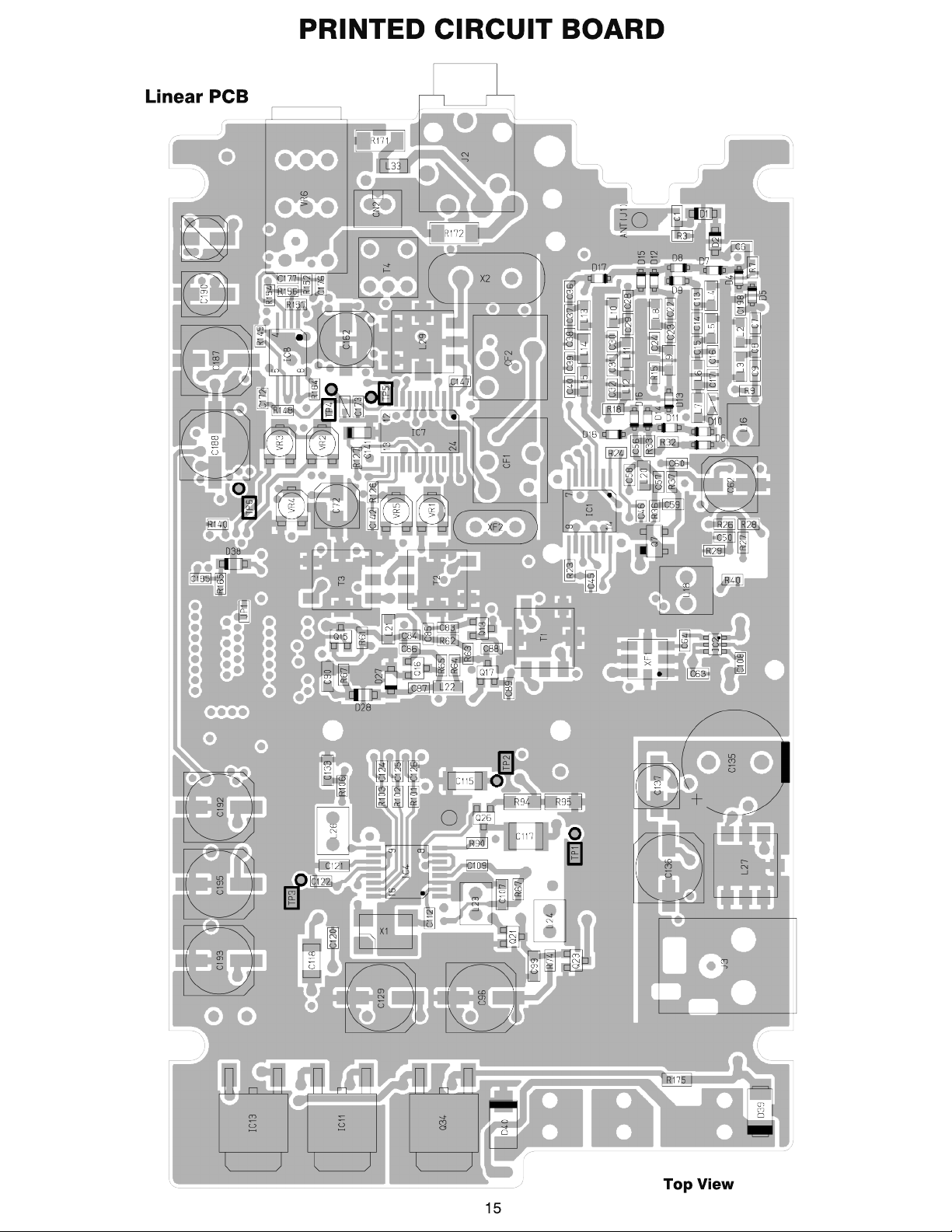
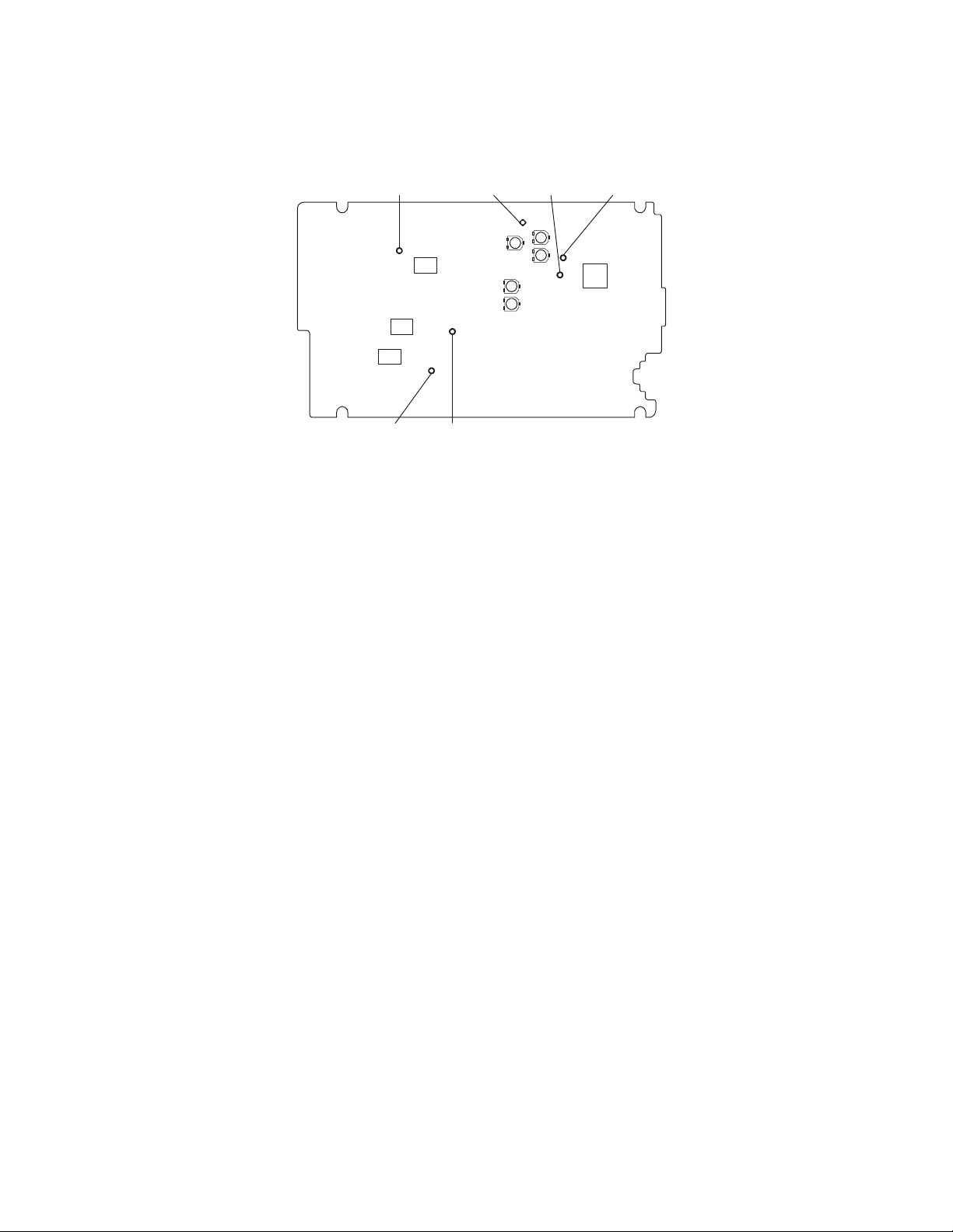
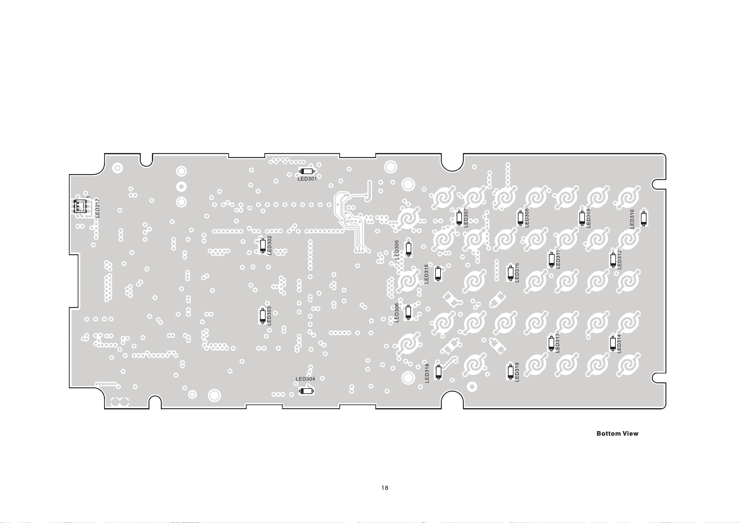
Linear PCB
PRINTED CIRCUIT BOARD
15
Top View
Page 16
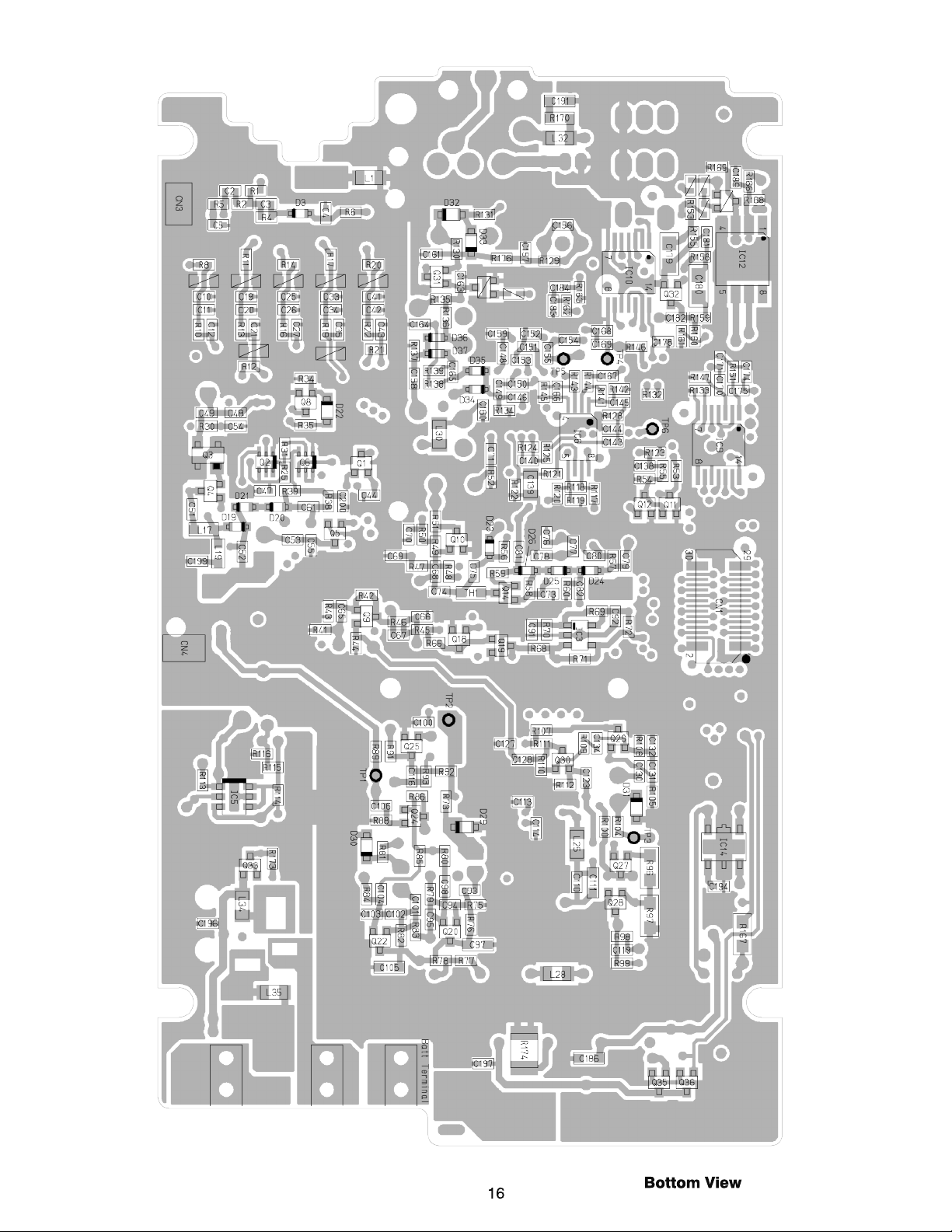
16
Bottom View
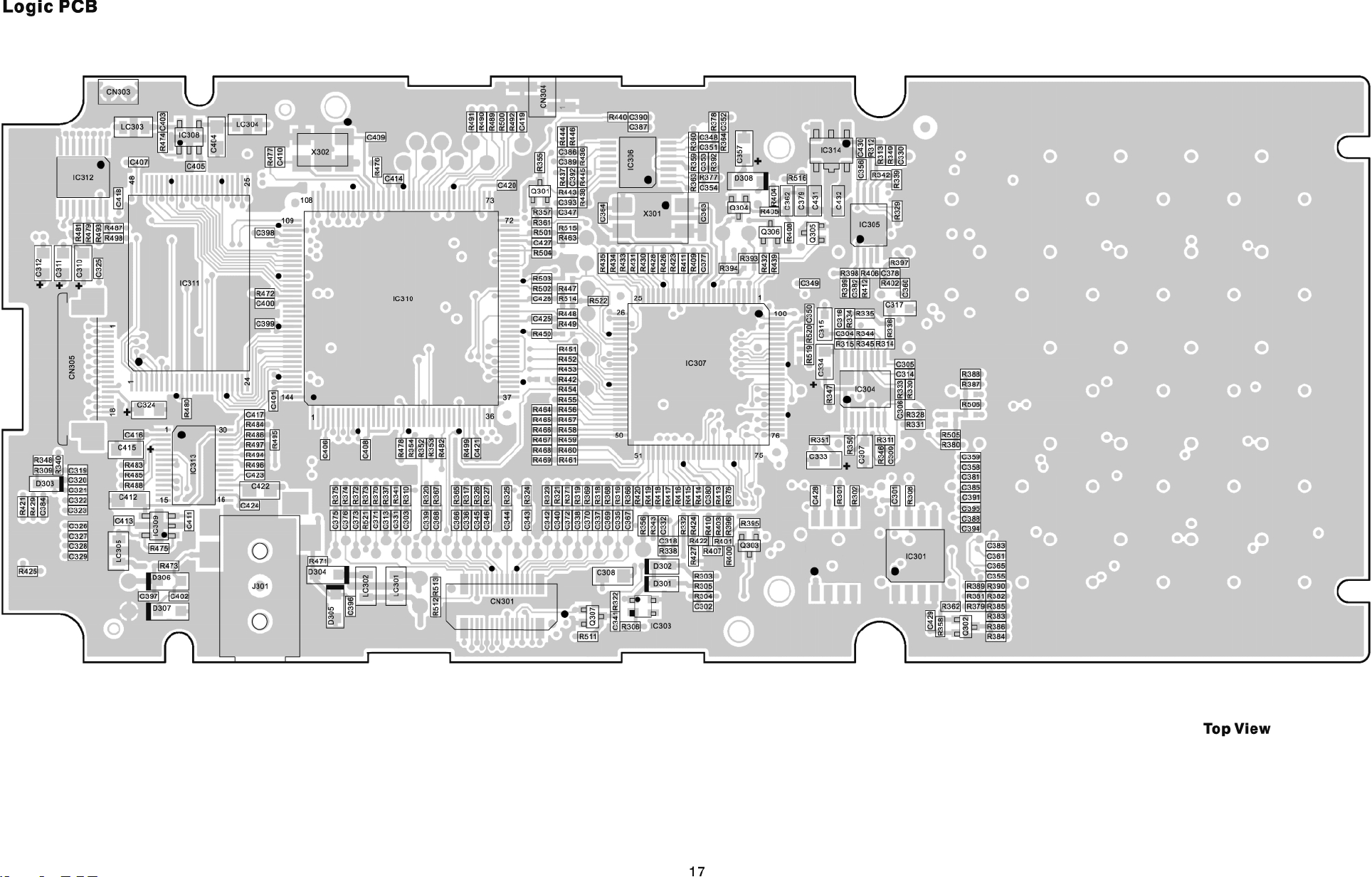
Page 17
Page 18
Page 19
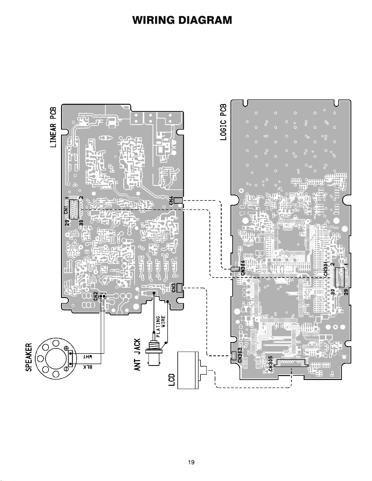
WIRING DIAGRAM
19
Page 20
EXPLODED VIEW for 20-106
To remove the rear case assembly,
unscrew four sc rews 18 .
15
10
14
c
a k
Sh
o
i
d
a
R
4
16
11
9
26
13
17
17
28
27
20
24
23
19
22
12
21
3
25
6
5
2
18
1
18
8
7
20
Page 21
MECHANICAL PARTS LIST
Ref. No. Description Mfr’s Part No.
1 Antenna, Rubber GE-04D-1050
2 Assembly, Case, Battery, Alkaline (Black) GA-05D-3550
or GA-99D-3329B
3 Assembly, Case, Battery, Rechargeable (Yellow) GA-05D-3680
or GA-99D-3326B
4 Assembly, Case, Front (Non-Repairable) GA-08D-0360
Case, Front GR-08A-0240
Window, LCD GR-08D-0250
Tape, Adhesive (L) GR-08D-0260
Tape, Adhesive (S) GR-08D-0530
Himelon, Speaker GR-08D-0570
Pipe, Light GR-07D-1610
5 Assembly, Case, Rear (Non-Repairable) GA-08D-1650
Case, Rear GR-06D-1080
or GE-04A-1133
Label, Model GR-08D-0391
6 Cap, Jack, Phone GR-07D-1560
7 Clip, Belt GR-06D-1120
8 Cover, Battery GR-06D-1091
9 Cushion, LCD GR-07D-1630
10 Holder, LCD GR-07D-0270
11 Key Top GR-08D-0280
12 Knob, Squelch GR-07D-1550
13 Knob, Volume GR-07D-1540
14 LCD GR-07D-0160
15 Reflector, LCD GR-07C-1620
16 Speaker 8-ohm 1W Max. GR-05D-3360
or 36A550-8B
Wire Housing Assembly Item No. 1
Hardware Kit #0801(B)
17 Screw, B P-tight 2x5 BLK Zn Bind P tight 2x5 BLK Zn
18 Screw, P P-tight 2.6x25 Zn P tight 2.6x25 Zn
19 See Electrical Parts List on Page 22.
20-25 See Electrical Parts List on Page 44.
26 See Electrical Parts List on Page 45.
27-28 See Electrical Parts List on Page 64.
21
Page 22
ELECTRICAL PARTS LIST
Ref. No. Description RS Part No. Mfr's Part No.
19 Assembly, PCB, Linear GA-08D-0020
Consists of the following:
Capacitors
C1 Ceramic 0.001 μF 50 V ±10% ECJ0EB1H102K
or ±5% or CM05B102J50AH
or ±10% or GRM155R71H102KA01D
C2 Ceramic 0.001 μF 50 V ±10% ECJ0EB1H102K
or ±5% or CM05B102J50AH
or ±10% or GRM155R71H102KA01D
C3 Ceramic 3 pF 50 V ±0.25 pF ECJ0EC1H030C
or CM05CH3R0C50AH
or GRM1555C1H3R0CZ01D
C4 Ceramic 0.001 μF 50 V ±10% ECJ0EB1H102K
or ±5% or CM05B102J50AH
or ±10% or GRM155R71H102KA01D
C5 Ceramic 0.001 μF 50 V ±10% ECJ0EB1H102K
or ±5% or CM05B102J50AH
or ±10% or GRM155R71H102KA01D
C6 Ceramic 0.001 μF 50 V ±10% ECJ0EB1H102K
or ±5% or CM05B102J50AH
or ±10% or GRM155R71H102KA01D
C7 Ceramic 5 pF 50 V ±0.25 pF ECJ0EC1H5R0C
or CM05CH5R0C50AH
or GRM1555C1H5R0CZ01D
C8 Ceramic 3 pF 50 V ±0.25 pF ECJ0EC1H030C
or CM05CH3R0C50AH
or GRM1555C1H3R0CZ01D
C9 Ceramic 5 pF 50 V ±0.25 pF ECJ0EC1H5R0C
or CM05CH5R0C50AH
or GRM1555C1H5R0CZ01D
C10 Ceramic 0.001 μF 50 V ±10% ECJ0EB1H102K
or ±5% or CM05B102J50AH
or ±10% or GRM155R71H102KA01D
C11 Ceramic 0.047 μF 10 V ±10% ECJ0EB1A473K
or ±5% or CM05B473J10AH
or ±10% or GRM155R71A473KA01D
C12 Ceramic 0.001 μF 50 V ±10% ECJ0EB1H102K
or ±5% or CM05B102J50AH
or ±10% or GRM155R71H102KA01D
C13 Ceramic 22 pF 50 V ±5% ECJ0EC1H220J
or CM05CH220J50AH
or GRM1555C1H220JZ01D
C14 Ceramic 6 pF 50 V ±0.5 pF ECJ0EC1H060D
or CM05CH6R0D50AH
or GRM1555C1H6R0DZ01D
C15 Ceramic 7 pF 50 V ±0.5 pF ECJ0EC1H070D
or CM05CH7R0D50AH
or GRM1555C1H7R0DZ01D
C16 Ceramic 2 pF 50 V ±0.25 pF ECJ0EC1H020C
or CM05CH2R0C50AH
or GRM1555C1H2R0CZ01D
C17 Ceramic 12 pF 50 V ±5% ECJ0EC1H120J
or CM05CH120J50AH
or GRM1555C1H120JZ01D
C18 Not used.
C19 Ceramic 0.001 μF 50 V ±0% ECJ0EB1H102K
or ±5% or CM05B102J50AH
or ±10% or GRM155R71H102KA01D
22
Page 23

Ref. No. Description RS Part No. Mfr's Part No.
C20 Ceramic 0.047 μF 10 V ±10% ECJ0EB1A473K
or ±5% or CM05B473J10AH
or ±10% or GRM155R71A473KA01D
C21 Ceramic 0.001 μF 50 V ±10% ECJ0EB1H102K
or ±5% or CM05B102J50AH
or ±10% or GRM155R71H102KA01D
C22 Ceramic 5 pF 50 V ±0.25 pF ECJ0EC1H5R0C
or CM05CH5R0C50AH
or GRM1555C1H5R0CZ01D
C23 Ceramic 5 pF 50 V ±0.25 pF ECJ0EC1H5R0C
or CM05CH5R0C50AH
or GRM1555C1H5R0CZ01D
C24 Ceramic 5 pF 50 V ±0.25 pF ECJ0EC1H5R0C
or CM05CH5R0C50AH
or GRM1555C1H5R0CZ01D
C25 Ceramic 0.001 μF 50 V ±10% ECJ0EB1H102K
or ±5% or CM05B102J50AH
or ±10% or GRM155R71H102KA01D
C26 Ceramic 0.047 μF 10 V ±10% ECJ0EB1A473K
or ±5% or CM05B473J10AH
or ±10% or GRM155R71A473KA01D
C27 Ceramic 0.001 μF 50 V ±10% ECJ0EB1H102K
or ±5% or CM05B102J50AH
or ±10% or GRM155R71H102KA01D
C28 Ceramic 33 pF 50 V ±5% ECJ0EC1H330J
or CM05CH330J50AH
or GRM1555C1H330JZ01D
C29 Ceramic 22 pF 50 V ±5% ECJ0EC1H220J
or CM05CH220J50AH
or GRM1555C1H220JZ01D
C30 Ceramic 10 pF 50 V ±0.5 pF ECJ0EC1H100D
or ±5% or CM05CH100J50AH
or GRM1555C1H100JZ01D
C31 Ceramic 15 pF 50 V ±5% ECJ0EC1H150J
or CM05CH150J50AH
or GRM1555C1H150JZ01D
C32 Ceramic 10 pF 50 V ±0.5 pF ECJ0EC1H100D
or ±5% or CM05CH100J50AH
or GRM1555C1H100JZ01D
C33 Ceramic 0.001 μF 50 V ±0% ECJ0EB1H102K
or ±5% or CM05B102J50AH
or ±10% or GRM155R71H102KA01D
C34 Ceramic 0.047 μF 10 V ±10% ECJ0EB1A473K
or ±5% or CM05B473J10AH
or ±10% or GRM155R71A473KA01D
C35 Ceramic 0.001 μF 50 V ±10% ECJ0EB1H102K
or ±5% or CM05B102J50AH
or ±10% or GRM155R71H102KA01D
C36 Ceramic 180 pF 50 V ±5% ECJ0EC1H181J
or CM05CH181J50AH
or GRM1555C1H181JA01D
C37 Ceramic 180 pF 50 V ±5% ECJ0EC1H181J
or CM05CH181J50AH
or GRM1555C1H181JA01D
C38 Ceramic 68 pF 50 V ±5% ECJ0EC1H680J
or CM05CH680J50AH
or GRM1555C1H680JZ01D
C39 Ceramic 120 pF 50 V ±5% ECJ0EC1H121J
or CM05CH121J50AH
or GRM1555C1H121JA01D
C40 Ceramic 68 pF 50 V ±5% ECJ0EC1H680J
or CM05CH680J50AH
or GRM1555C1H680JZ01D
23
Page 24

Ref. No. Description RS Part No. Mfr's Part No.
C41 Ceramic 0.001 μF 50 V ±10% ECJ0EB1H102K
or ±5% or CM05B102J50AH
or ±10% or GRM155R71H102KA01D
C42 Ceramic 0.047 μF 10 V ±10% ECJ0EB1A473K
or ±5% or CM05B473J10AH
or ±10% or GRM155R71A473KA01D
C43 Ceramic 0.001 μF 50 V ±10% ECJ0EB1H102K
or ±5% or CM05B102J50AH
or ±10% or GRM155R71H102KA01D
C44 Ceramic 0.047 μF 10 V ±10% ECJ0EB1A473K
or ±5% or CM05B473J10AH
or ±10% or GRM155R71A473KA01D
C45 Ceramic 47 pF 50 V ±5% ECJ0EC1H470J
or CM05CH470J50AH
or GRM1555C1H470JZ01D
C46 Ceramic 47 pF 50 V ±5% ECJ0EC1H470J
or CM05CH470J50AH
or GRM1555C1H470JZ01D
C47 Ceramic 0.001 μF 50 V ±10% ECJ0EB1H102K
or ±5% or CM05B102J50AH
or ±10% or GRM155R71H102KA01D
C48 Ceramic 2 pF 50 V ±0.25 pF ECJ0EC1H020C
or CM05CH2R0C50AH
or GRM1555C1H2R0CZ01D
C49 Ceramic 3 pF 50 V ±0.25 pF ECJ0EC1H030C
or CM05CH3R0C50AH
or GRM1555C1H3R0CZ01D
C50 Ceramic 22 pF 50 V ±5% ECJ0EC1H220J
or CM05CH220J50AH
or GRM1555C1H220JZ01D
C51 Ceramic 5 pF 50 V ±0.25 pF ECJ0EC1H5R0C
or CM05CH5R0C50AH
or GRM1555C1H5R0CZ01D
C52 Ceramic 0.001 μF 50 V ±0% ECJ0EB1H102K
or ±5% or CM05B102J50AH
or ±10% or GRM155R71H102KA01D
C53 Ceramic 3 pF 50 V ±0.25 pF ECJ0EC1H030C
or CM05CH3R0C50AH
or GRM1555C1H3R0CZ01D
C54 Ceramic 0.001 μF 50 V ±0% ECJ0EB1H102K
or ±5% or CM05B102J50AH
or ±10% or GRM155R71H102KA01D
C55 Ceramic 3 pF 50 V ±0.25 pF ECJ0EC1H030C
or CM05CH3R0C50AH
or GRM1555C1H3R0CZ01D
C56 Ceramic 0.001 μF 50 V ±0% ECJ0EB1H102K
or ±5% or CM05B102J50AH
or ±10% or GRM155R71H102KA01D
C57 Ceramic 1 pF 50 V ±0.25 pF ECJ0EC1H1R0C
or CM05CH1R0C50AH
or GRM1555C1H1R0CZ01D
C58 Ceramic 5 pF 50 V ±0.25 pF ECJ0EC1H5R0C
or CM05CH5R0C50AH
or GRM1555C1H5R0CZ01D
C59 Ceramic 0.001 μF 50 V ±10% ECJ0EB1H102K
or ±5% or CM05B102J50AH
or ±10% or GRM155R71H102KA01D
C60 Ceramic 0.001 μF 50 V ±10% ECJ0EB1H102K
or ±5% or CM05B102J50AH
or ±10% or GRM155R71H102KA01D
C61 Ceramic 100 pF 50 V ±5% ECJ0EC1H101J
or CM05CH101J50AH
or GRM1555C1H101JZ01D
C62 Electrolytic 33 μF 10 V ±20% 1AECBS330M
24
Page 25

Ref. No. Description RS Part No. Mfr's Part No.
C63 Ceramic 0.001 μF 50 V ±10% ECJ0EB1H102K
or ±5% or CM05B102J50AH
or ±10% or GRM155R71H102KA01D
C64 Ceramic 0.001 μF 50 V ±10% ECJ0EB1H102K
or ±5% or CM05B102J50AH
or ±10% or GRM155R71H102KA01D
C65 Ceramic 0.001 μF 50 V ±10% ECJ0EB1H102K
or ±5% or CM05B102J50AH
or ±10% or GRM155R71H102KA01D
C66 Ceramic 0.001 μF 50 V ±10% ECJ0EB1H102K
or ±5% or CM05B102J50AH
or ±10% or GRM155R71H102KA01D
C67 Ceramic 33 pF 50 V ±5% ECJ0EC1H330J
or CM05CH330J50AH
or GRM1555C1H330JZ01D
C68 Ceramic 0.001 μF 50 V ±0% ECJ0EB1H102K
or ±5% or CM05B102J50AH
or ±10% or GRM155R71H102KA01D
C69 Ceramic 0.001 μF 50 V ±10% ECJ0EB1H102K
or ±5% or CM05B102J50AH
or ±10% or GRM155R71H102KA01D
C70 Ceramic 0.001 μF 50 V ±10% ECJ0EB1H102K
or ±5% or CM05B102J50AH
or ±10% or GRM155R71H102KA01D
C71 Ceramic 0.001 μF 50 V ±10% ECJ0EB1H102K
or ±5% or CM05B102J50AH
or ±10% or GRM155R71H102KA01D
C72 Electrolytic 1 μF 50 V ±20% 1HECBS1R0M
C73 Ceramic 0.001 μF 50 V ±0% ECJ0EB1H102K
or ±5% or CM05B102J50AH
or ±10% or GRM155R71H102KA01D
C74 Ceramic 0.001 μF 50 V ±10% ECJ0EB1H102K
or ±5% or CM05B102J50AH
or ±10% or GRM155R71H102KA01D
C75 Ceramic 68 pF 50 V ±5% ECJ0EC1H680J
or CM05CH680J50AH
or GRM1555C1H680JZ01D
C76 Ceramic 39 pF 50 V ±5% ECJ0EC1H390J
or CM05CH390J50AH
or GRM1555C1H390JZ01D
C77 Ceramic 1.5 pF 50 V ±0.25 pF ECJ0EC1H1R5C
or CM05CH1R5C50AH
or GRM1555C1H1R5CZ01D
C78 Ceramic 39 pF 50 V ±5% ECJ0EC1H390J
or CM05CH390J50AH
or GRM1555C1H390JZ01D
C79 Ceramic 0.001 μF 50 V ±0% ECJ0EB1H102K
or ±5% or CM05B102J50AH
or ±10% or GRM155R71H102KA01D
C80 Ceramic 0.001 μF 50 V ±10% ECJ0EB1H102K
or ±5% or CM05B102J50AH
or ±10% or GRM155R71H102KA01D
C81 Ceramic 0.01 μF 16 V ±10% ECJ0EB1C103K
or ±5% or CM05B103J16AH
or ±10% or GRM155R71C103KA01D
C82 Ceramic 0.01 μF 16 V ±10% ECJ0EB1C103K
or ±5% or CM05B103J16AH
or ±10% or GRM155R71C103KA01D
C83 Ceramic 0.047 μF 10 V ±10% ECJ0EB1A473K
or ±5% or CM05B473J10AH
or ±10% or GRM155R71A473KA01D
C84 Ceramic 56 pF 50 V ±5% ECJ0EC1H560J
or CM05CH560J50AH
or GRM1555C1H560JZ01D
25
Page 26

Ref. No. Description RS Part No. Mfr's Part No.
C85 Ceramic 0.001 μF 50 V ±10% ECJ0EB1H102K
or ±5% or CM05B102J50AH
or ±10% or GRM155R71H102KA01D
C86 Ceramic 0.01 μF 16 V ±10% ECJ0EB1C103K
or ±5% or CM05B103J16AH
or ±10% or GRM155R71C103KA01D
C87 Ceramic 0.01 μF 16 V ±10% ECJ0EB1C103K
or ±5% or CM05B103J16AH
or ±10% or GRM155R71C103KA01D
C88 Ceramic 0.047 μF 10 V ±10% ECJ0EB1A473K
or ±5% or CM05B473J10AH
or ±10% or GRM155R71A473KA01D
C89 Ceramic 0.047 μF 10 V ±10% ECJ0EB1A473K
or ±5% or CM05B473J10AH
or ±10% or GRM155R71A473KA01D
C90 Ceramic 0.47 μF 10 V ±10% ECJ1VB1A474K
or 6.3 V or ECJ1VB0J474K
or 10 V or LMK107BJ474KA-T
or GRM188R61A474KA61D
C91 Ceramic 0.047 μF 10 V ±10% ECJ0EB1A473K
or ±5% or CM05B473J10AH
or ±10% or GRM155R71A473KA01D
C92 Ceramic 0.01 μF 16 V ±10% ECJ0EB1C103K
or ±5% or CM05B103J16AH
or ±10% or GRM155R71C103KA01D
C93 Ceramic 220 pF 50 V ±5% ECJ0EC1H221J
or CM05CH221J50AH
or GRM1555C1H221JA01D
C94 Ceramic 15 pF 50 V ±5% ECJ0EC1H150J
or CM05CH150J50AH
or GRM1555C1H150JZ01D
C95 Ceramic 8 pF 50 V ±0.5 pF ECJ0EC1H080D
or CM05CH8R0D50AH
or GRM1555C1H8R0DZ01D
C96 Electrolytic 220 μF 6.3 V ±20% 0JECBS221M
C97 Ceramic 0.001 μF 50 V ±% ECJ1VC1H102J
or CM105CH102J50AT
or GRM1885C1H102JA01D
C98 Ceramic 3 pF 50 V ±0.25 pF ECJ0EC1H030C
or CM05CH3R0C50AH
or GRM1555C1H3R0CZ01D
C99 Ceramic 0.001 μF 50 V ±5% ECJ1VC1H102J
or CM105CH102J50AT
or GRM1885C1H102JA01D
C100 Ceramic 47 pF 50 V ±5% ECJ0EC1H470J
or CM05CH470J50AH
or GRM1555C1H470JZ01D
C101 Ceramic 100 pF 50 V ±5% ECJ0EC1H101J
or CM05CH101J50AH
or GRM1555C1H101JZ01D
C102 Ceramic 12 pF 50 V ±5% ECJ0EC1H120J
or CM05CH120J50AH
or GRM1555C1H120JZ01D
C103 Ceramic 5 pF 50 V ±0.25 pF ECJ0EC1H5R0C
or CM05CH5R0C50AH
or GRM1555C1H5R0CZ01D
C104 Ceramic 2 pF 50 V ±0.25 pF ECJ0EC1H020C
or CM05CH2R0C50AH
or GRM1555C1H2R0CZ01D
C105 Ceramic 0.001 μF 50 V ±5% ECJ1VC1H102J
or CM105CH102J50AT
or GRM1885C1H102JA01D
C106 Ceramic 100 pF 50 V ±5% ECJ0EC1H101J
or CM05CH101J50AH
or GRM1555C1H101JZ01D
26
Page 27

Ref. No. Description RS Part No. Mfr's Part No.
C107 Ceramic 0.001 μF 50 V ±5% ECJ1VC1H102J
or CM105CH102J50AT
or GRM1885C1H102JA01D
C108 Ceramic 100 pF 50 V ±5% ECJ0EC1H101J
or CM05CH101J50AH
or GRM1555C1H101JZ01D
C109 Ceramic 100 pF 50 V ±5% ECJ0EC1H101J
or CM05CH101J50AH
or GRM1555C1H101JZ01D
C110 Ceramic 100 pF 50 V ±5% ECJ0EC1H101J
or CM05CH101J50AH
or GRM1555C1H101JZ01D
C111 Ceramic 0.001 μF 50 V ±5% ECJ1VC1H102J
or CM105CH102J50AT
or GRM1885C1H102JA01D
C112 Ceramic 100 pF 50 V ±5% ECJ0EC1H101J
or CM05CH101J50AH
or GRM1555C1H101JZ01D
C113 Ceramic 0.1 μF 10 V ±10% ECJ0EB1A104K
or ±5% or CM05B104J10AH
or ±10% or GRM155R71A104KA01D
C114 Ceramic 33 pF 50 V ±5% ECJ0EC1H330J
or CM05CH330J50AH
or GRM1555C1H330JZ01D
C115 Metalized PPS Film 0.0033 μF 50 V ±5% ECHU1H332JX5
C116 Ceramic 0.0022 μF 50 V ±10% ECJ0EB1H222K
or ±5% or CM05B222J50AH
or ±10% or GRM155R71H222KA01D
C117 Metalized PPS Film 0.033 μF 50 V ±5% ECHU1H333JX5
C118 Metalized PPS Film 0.047 μF 16 V ±5% ECHU1C473JX5
C119 Ceramic 0.01 μF 16 V ±0% ECJ0EB1C103K
or ±5% or CM05B103J16AH
or ±10% or GRM155R71C103KA01D
C120 Ceramic 0.01 μF 16 V ±10% ECJ0EB1C103K
or ±5% or CM05B103J16AH
or ±10% or GRM155R71C103KA01D
C121 Ceramic 0.001 μF 50 V ±5% ECJ1VC1H102J
or CM105CH102J50AT
or GRM1885C1H102JA01D
C122 Ceramic 0.1 μF 10 V ±10% ECJ0EB1A104K
or ±5% or CM05B104J10AH
or ±10% or GRM155R71A104KA01D
C123 Ceramic 100 pF 50 V ±5% ECJ0EC1H101J
or CM05CH101J50AH
or GRM1555C1H101JZ01D
C124 Ceramic 47 pF 50 V ±5% ECJ0EC1H470J
or CM05CH470J50AH
or GRM1555C1H470JZ01D
C125 Ceramic 47 pF 50 V ±5% ECJ0EC1H470J
or CM05CH470J50AH
or GRM1555C1H470JZ01D
C126 Ceramic 47 pF 50 V ±5% ECJ0EC1H470J
or CM05CH470J50AH
or GRM1555C1H470JZ01D
C127 Ceramic 10 pF 50 V ±0.5 pF ECJ0EC1H100D
or ±5% or CM05CH100J50AH
or GRM1555C1H100JZ01D
C128
C129 Electrolytic 220 μF 6.3 V ±20% 0JECBS221M
C130 Ceramic 22 pF 50 V ±5% ECJ0EC1H220J
Ceramic 10 pF 50 V ±0.5 pF ECJ0EC1H100D
or ±5% or CM05CH100J50AH
or GRM1555C1H100JZ01D
or CM05CH220J50AH
or GRM1555C1H220JZ01D
27
Page 28

Ref. No. Description RS Part No. Mfr's Part No.
C131 Ceramic 15 pF 50 V ±5% ECJ0EC1H150J
or CM05CH150J50AH
or GRM1555C1H150JZ01D
C132 Ceramic 7 pF 50 V ±0.5 pF ECJ0EC1H070D
or CM05CH7R0D50AH
or GRM1555C1H7R0DZ01D
C133 Ceramic 0.001 μF 50 V ±% ECJ1VC1H102J
or CM105CH102J50AT
or GRM1885C1H102JA01D
C134 Ceramic 5 pF 50 V ±0.25 pF ECJ0EC1H5R0C
or CM05CH5R0C50AH
or GRM1555C1H5R0CZ01D
C135 Electrolytic 1000 μF 16 V ±20% UVK1C102MPD
C136 Electrolytic 33 μF 35 V ±20% 1VECBS330M
C137 Electrolytic 4.7 μF 35 V ±20% 1VECBS4R7M
C138 Ceramic 0.01 μF 16 V ±10% ECJ0EB1C103K
or ±5% or CM05B103J16AH
or ±10% or GRM155R71C103KA01D
C139 Metalized PPS Film 0.022 μF 50 V ±5% ECHU1H223JX5
C140 Ceramic 12 pF 50 V ±5% ECJ0EC1H120J
or CM05CH120J50AH
or GRM1555C1H120JZ01D
C141 Tantalum 10 μF 10 V ±20% TCP1A106M8R
or TESVSP1A106M8R
or TEESVP1A106M8R
or F921A106MPA
C142 Ceramic 0.01 μF 16 V ±10% ECJ0EB1C103K
or ±5% or CM05B103J16AH
or ±10% or GRM155R71C103KA01D
C143 Ceramic 220 pF 50 V ±5% ECJ0EC1H221J
or CM05CH221J50AH
or GRM1555C1H221JA01D
C144 Ceramic 220 pF 50 V ±5% ECJ0EC1H221J
or CM05CH221J50AH
or GRM1555C1H221JA01D
C145 Ceramic 220 pF 50 V ±5% ECJ0EC1H221J
or CM05CH221J50AH
or GRM1555C1H221JA01D
C146 Ceramic 0.01 μF 16 V ±10% ECJ0EB1C103K
or ±5% or CM05B103J16AH
or ±10% or GRM155R71C103KA01D
C147 Ceramic 56 pF 50 V ±5% ECJ0EC1H560J
or CM05CH560J50AH
or GRM1555C1H560JZ01D
C148 Ceramic 82 pF 50 V ±5% ECJ0EC1H820J
or CM05CH820J50AH
or GRM1555C1H820JZ01D
C149 Ceramic 0.01 μF 16 V ±0% ECJ0EB1C103K
or ±5% or CM05B103J16AH
or ±10% or GRM155R71C103KA01D
C150 Ceramic 0.01 μF 16 V ±10% ECJ0EB1C103K
or ±5% or CM05B103J16AH
or ±10% or GRM155R71C103KA01D
C151 Ceramic 0.1 μF 10 V ±10% ECJ0EB1A104K
or ±5% or CM05B104J10AH
or ±10% or GRM155R71A104KA01D
C152 Ceramic 0.1 μF 10 V ±10% ECJ0EB1A104K
or ±5% or CM05B104J10AH
or ±10% or GRM155R71A104KA01D
C153 Ceramic 0.1 μF 10 V ±10% ECJ0EB1A104K
or ±5% or CM05B104J10AH
or ±10% or GRM155R71A104KA01D
C154 Ceramic 10 pF 50 V ±0.5 pF ECJ0EC1H100D
or ±5% or CM05CH100J50AH
or GRM1555C1H100JZ01D
28
Page 29

Ref. No. Description RS Part No. Mfr's Part No.
C155 Ceramic 0.01 μF 16 V ±10% ECJ0EB1C103K
or ±5% or CM05B103J16AH
or ±10% or GRM155R71C103KA01D
C156 Ceramic 180 pF 50 V ±5% ECJ0EC1H181J
or CM05CH181J50AH
or GRM1555C1H181JA01D
C157 Ceramic 0.1 μF 10 V ±10% ECJ0EB1A104K
or ±5% or CM05B104J10AH
or ±10% or GRM155R71A104KA01D
C158 Ceramic 0.01 μF 16 V ±10% ECJ0EB1C103K
or ±5% or CM05B103J16AH
or ±10% or GRM155R71C103KA01D
C159 Ceramic 0.1 μF 10 V ±10% ECJ0EB1A104K
or ±5% or CM05B104J10AH
or ±10% or GRM155R71A104KA01D
C160 Ceramic 0.1 μF 10 V ±10% ECJ0EB1A104K
or ±5% or CM05B104J10AH
or ±10% or GRM155R71A104KA01D
C161 Ceramic 0.1 μF 10 V ±10% ECJ0EB1A104K
or ±5% or CM05B104J10AH
or ±10% or GRM155R71A104KA01D
C162 Electrolytic 47 μF 6.3 V ±20% 0JECBS470M
C163 Ceramic 0.001 μF 50 V ±0% ECJ0EB1H102K
or ±5% or CM05B102J50AH
or ±10% or GRM155R71H102KA01D
C164 Ceramic 0.001 μF 50 V ±10% ECJ0EB1H102K
or ±5% or CM05B102J50AH
or ±10% or GRM155R71H102KA01D
C165 Ceramic 0.01 μF 16 V ±10% ECJ0EB1C103K
or ±5% or CM05B103J16AH
or ±10% or GRM155R71C103KA01D
C166 Ceramic 0.01 μF 16 V ±10% ECJ0EB1C103K
or ±5% or CM05B103J16AH
or ±10% or GRM155R71C103KA01D
C167 Ceramic 220 pF 50 V ±5% ECJ0EC1H221J
or CM05CH221J50AH
or GRM1555C1H221JA01D
C168 Ceramic 100 pF 50 V ±5% ECJ0EC1H101J
or CM05CH101J50AH
or GRM1555C1H101JZ01D
C169 Ceramic 220 pF 50 V ±5% ECJ0EC1H221J
or CM05CH221J50AH
or GRM1555C1H221JA01D
C170 Ceramic 0.0047 μF 16 V ±10% ECJ0EB1C472K
or ±5% or CM05B472J16AH
or ±10% or GRM155R71C472KA01D
or 50 V or GRM155R71H472KA01D
C171 Ceramic 0.022 μF 16 V ±10% ECJ0EB1C223K
or ±5% or CM05B223J16AH
or ±10% or GRM155R71C223KA01D
C172 Ceramic 33 pF 50 V ±5% ECJ0EC1H330J
or CM05CH330J50AH
or GRM1555C1H330JZ01D
C173 Ceramic 0.0047 μF 16 V ±0% ECJ0EB1C472K
or ±5% or CM05B472J16AH
or ±10% or GRM155R71C472KA01D
or 50 V or GRM155R71H472KA01D
C174 Ceramic 820 pF 50 V ±0% ECJ0EB1H821K
or ±5% or CM05B821J50AH
or ±10% or GRM155R71H821KA01D
C175 Ceramic 0.01 μF 16 V ±10% ECJ0EB1C103K
or ±5% or CM05B103J16AH
or ±10% or GRM155R71C103KA01D
29
Page 30

Ref. No. Description RS Part No. Mfr's Part No.
C176 Ceramic 0.022 μF 16 V ±10% ECJ0EB1C223K
or ±5% or CM05B223J16AH
or ±10% or GRM155R71C223KA01D
C177 Ceramic 0.022 μF 16 V ±10% ECJ0EB1C223K
or ±5% or CM05B223J16AH
or ±10% or GRM155R71C223KA01D
C178 Ceramic 0.01 μF 16 V ±10% ECJ0EB1C103K
or ±5% or CM05B103J16AH
or ±10% or GRM155R71C103KA01D
C179 Ceramic 10 μF 6.3 V ±10% JMK212X5R106KG-T
or JMK212BJ106KG-T
or 10 V or GRM21BR61A106KE19L
C180 Ceramic 1 μF 10 V ±10% ECJ2FB1A105K
or LMK212BJ105KG-T
or GRM21BR71A105KA01L
C181 Ceramic 0.01 μF 16 V ±10% ECJ0EB1C103K
or ±5% or CM05B103J16AH
or ±10% or GRM155R71C103KA01D
C182 Ceramic 0.01 μF 16 V ±10% ECJ0EB1C103K
or ±5% or CM05B103J16AH
or ±10% or GRM155R71C103KA01D
C183 Ceramic 0.022 μF 16 V ±10% ECJ0EB1C223K
or ±5% or CM05B223J16AH
or ±10% or GRM155R71C223KA01D
C184 Ceramic 0.01 μF 16 V ±10% ECJ0EB1C103K
or ±5% or CM05B103J16AH
or ±10% or GRM155R71C103KA01D
C185 Ceramic 0.001 μF 50 V ±10% ECJ0EB1H102K
or ±5% or CM05B102J50AH
or ±10% or GRM155R71H102KA01D
C186 Ceramic 0.33 μF 10 V ±10% ECJ1VB1A334K
or 6.3 V or ECJ1VB0J334K
or 10 V or LMK107BJ334KA-T
or GRM188R71A334KA61D
C187 Electrolytic 220 μF 6.3 V ±20% 0JECBS221M
C188 Electrolytic 220 μF 6.3 V ±20% 0JECBS221M
C189 Ceramic 0.022 μF 16 V ±0% ECJ0EB1C223K
or ±5% or CM05B223J16AH
or ±10% or GRM155R71C223KA01D
C190 Electrolytic 10 μF 16 V ±20% 1CECBS100M
C191 Ceramic 0.22 μF 10 V ±0% ECJ1VB1A224K
or 50 V or ±5% or CM105X7R224J50AT
or 10 V or ±10% or GRM188R71A224KA01D
or 16V or EMK107BJ224KA-T
C192 Electrolytic 220 μF 6.3 V ±20% 0JECBS221M
C193 Electrolytic 220 μF 16 V ±20% 1CECBS221M
C194
C195 Electrolytic 220 μF 6.3 V ±20% 0JECBS221M
C196 Ceramic 0.001 μF 50 V ±0% ECJ0EB1H102K
C197 Ceramic 0.01 μF 16 V ±10% ECJ0EB1C103K
C198 Ceramic 2 pF 50 V ±0.25 pF ECJ0EC1H020C
C199 Ceramic 12 pF 50 V ±5% ECJ0EC1H120J
C200 Ceramic 0.001 μF 50 V ±0% ECJ0EB1H102K
Ceramic 0.1 μF 10 V ±0% ECJ0EB1A104K
or ±5% or CM05B104J10AH
or ±10% or GRM155R71A104KA01D
or ±5% or CM05B102J50AH
or ±10% or GRM155R71H102KA01D
or ±5% or CM05B103J16AH
or ±10% or GRM155R71C103KA01D
or CM05CH2R0C50AH
or GRM1555C1H2R0CZ01D
or CM05CH120J50AH
or GRM1555C1H120JZ01D
or ±5% or CM05B102J50AH
or ±10% or GRM155R71H102KA01D
30
Page 31

Ref. No. Description RS Part No. Mfr's Part No.
Ceramic Filters
CF1 455 kHz CFULA455KF1Y-B0
CF2 455 kHz SFPS455H
or LT455HTU
Connectors
CN1 30-pin, Male AXK6S3064BV1
CN2 2-pin, Male IL-Y-2P-S15T2-EF(pb Free)
or IL-Y-2P-S15T2-EF
CN3 2-pin, Male 20010S-02G2T
CN4 2-pin, Male 20010S-02G2T
Diodes
D1 HVU131-TR-F-E Marked P1 Silicon HVU131-TR-F-E
D2 HVU131-TR-F-E Marked P1 Silicon HVU131-TR-F-E
D3 HSC277-TR-F-E Silicon HSC277-TR-F-E
D4 HSC277-TR-F-E Silicon HSC277-TR-F-E
D5 HSC277-TR-F-E Silicon HSC277-TR-F-E
D6 HSC277-TR-F-E Silicon HSC277-TR-F-E
D7 HSC277-TR-F-E Silicon HSC277-TR-F-E
D8 HSC277-TR-F-E Silicon HSC277-TR-F-E
D9 HSC277-TR-F-E Silicon HSC277-TR-F-E
D10 HSC277-TR-F-E Silicon HSC277-TR-F-E
D11 HSC277-TR-F-E Silicon HSC277-TR-F-E
D12 HSC277-TR-F-E Silicon HSC277-TR-F-E
D13 HSC277-TR-F-E Silicon HSC277-TR-F-E
D14 HSC277-TR-F-E Silicon HSC277-TR-F-E
D15 HSC277-TR-F-E Silicon HSC277-TR-F-E
D16 HSC277-TR-F-E Silicon HSC277-TR-F-E
D17 HSC277-TR-F-E Silicon HSC277-TR-F-E
D18 HSC277-TR-F-E Silicon HSC277-TR-F-E
D19 HSC277-TR-F-E Silicon HSC277-TR-F-E
D20 HSC277-TR-F-E Silicon HSC277-TR-F-E
D21 HSC277-TR-F-E Silicon HSC277-TR-F-E
D22 1SS355F-TE17 Marked A Silicon 1SS355F-TE17
or 1SS355TE-17 or 1SS355TE-17
D23 HSC277-TR-F-E Silicon HSC277-TR-F-E
D24 HSC277-TR-F-E Silicon HSC277-TR-F-E
D25 HSC277-TR-F-E Silicon HSC277-TR-F-E
D26 HSC277-TR-F-E Silicon HSC277-TR-F-E
D27 1SS357(TPH3,F) Marked S3 Silicon 1SS357(TPH3,F)
or 1SS355F-TE17 or 1SS355F-TE17
D28 1SS357(TPH3,F) Marked S3 Silicon 1SS357(TPH3,F)
or 1SS355F-TE17 or 1SS355F-TE17
D29 HVU300A-TR-U-E Marked O Silicon HVU300A-TR-U-E
D30 HVU300A-TR-U-E Marked O Silicon HVU300A-TR-U-E
D31 HVU300A-TR-U-E Marked O Silicon HVU300A-TR-U-E
D32 HVU17-TR-U-E Marked E Silicon HVU17-TR-U-E
D33 HVU17-TR-U-E Marked E Silicon HVU17-TR-U-E
D34 HSC277-TR-F-E Silicon HSC277-TR-F-E
D35 HSC277-TR-F-E Silicon HSC277-TR-F-E
D36 HSC277-TR-F-E Silicon HSC277-TR-F-E
D37 HSC277-TR-F-E Silicon HSC277-TR-F-E
D38 1SS355F-TE17 Marked A Silicon 1SS355F-TE17
or 1SS355TE-17 or 1SS355TE-17
D39 FM4003-T Silicon FM4003-T
or FM4004-T or FM4004-T
D40 RB060L-40TE25 Marked 36 Silicon RB060L-40TE25
31
Page 32

Ref. No. Description RS Part No. Mfr's Part No.
Integrated Circuits
IC1 HD74AC164TELL-E Band Select/Attenuator, MOS SMT HD74AC164TELL-E
or TC74VHC164FT-EL,F or TC74VHC164FT-EL,F
or HD74AC164TELL or HD74AC164TELL
or TC74VHC164FT-EL or TC74VHC164FT-EL
IC2 μPC2757TB-E3-A 1st Mixer MOS SMT μPC2757TB-E3-A
or μPC2757TB or μPC2757TB
IC3 NJM2406F-TE1(pbF) Detector Bipolar SMT NJM2406F-TE1(pbF)
IC4 MB15F07SLPFV1-BND-EF-6E1 PLL, MOS SMT MB15F07SLPFV1-BND-EF-6E1
or MB15F07SLPFV1-BND or MB15F07SLPFV1-BND
IC5 TK11819MTL-G DC-DC Converter Bipolar SMT TK11819MTL-G
or TK11819MTL or TK11819MTL
IC6 NJM2904V-TE1(pbF) Noise Amp. Bipolar SMT NJM2904V-TE1(pbF)
IC7 TK10931V-TL-G 3rd IF Amp./3rd Local Mixer/Quad. TK10931V-TL-G
or TK10931V-TL Bipolar SMT or TK10931V-TL
IC8 NJM13404V-TE1(pbF) Buffer/Pre Amp. Bipolar SMT NJM13404V-TE1(pbF)
IC9 TC74HC4066AFT(EL),(F) Switching MOS SMT TC74HC4066AFT(EL),(F)
or TC74HC4066AFT(EL) or TC74HC4066AFT(EL)
or TC74HC4066AFS-TE1608 or TC74HC4066AFS-TE1608
IC10 TC74HC4066AFT(EL),(F) Mute/Switching MOS SMT TC74HC4066AFT(EL),(F)
or TC74HC4066AFT(EL) or TC74HC4066AFT(EL)
or TC74HC4066AFS-TE1608 or TC74HC4066AFS-TE1608
IC11 BA05FP-E2 Voltage Regulator Bipolar SMT BA05FP-E2
or BA05CC0FP-E2 or BA05CC0FP-E2
IC12 NJM2070M-TE1(pbF) Audio Amp. Bipolar SMT NJM2070M-TE1(pbF)
IC13 AN77033SP-E1 Voltage Regulator Bipolar SMT AN77033SP-E1
IC14 TK11233CUCB-G Regulator Switching, Bipolar SMT TK11233CUCB-G
or TK11233BUCB-G or TK11233BUCB-G
or TK11233CUCB or TK11233CUCB
or TK11233BUCB-G or TK11233BUCB-G
Jacks
J1 Jack Antenna G-BNC-KD104
or GE-02D-8220
or GE-85D-5383
J2 Jack, Earphone HSJ1493-0100109
or HSJ1493-01-010
J3 Jack, Power HEC3110-01-010
Coils
L1 Choke 1 μH LBC2012T1R0M
L2 LPF (764-1300MHz) 3.9 nH HK1608 3N9S-T
or LL1608-LFS3N9S
L3 LPF (764-1300MHz) 3.9 nH HK1608 3N9S-T
or LL1608-LFS3N9S
L4 LPF (406-512MHz) 8.2 nH HK1608 8N2J-T
or LL1608-LFS8N2J
L5 LPF (406-512MHz) 8.2 nH HK1608 8N2J-T
or LL1608-LFS8N2J
L6 LPF (406-512MHz) 18 nH HK1608 18NJ-T
or LL1608-LFS18NJ
L7 LPF (406-512MHz) 18 nH HK1608 18NJ-T
or LL1608-LFS18NJ
L8 LPF (225-406MHz) 47 nH HK1608 47NJ-T
or LL1608-LFS47NJ
L9 LPF (225-406MHz) 47 nH HK1608 47NJ-T
or LL1608-LFS47NJ
32
Page 33

Ref. No. Description RS Part No. Mfr's Part No.
L10 LPF (108-225MHz) 56 nH HK1608 56NJ-T
or LL1608-LFS56NJ
L11 LPF (108-225MHz) 82 nH HK1608 82NJ-T
or LL1608-LFS82NJ
L12 LPF (108-225MHz) 82 nH HK1608 82NJ-T
or LL1608-LFS82NJ
L13 LPF (25-54MHz) 0.22 μH LK1608 R22K-T
or LL1608-LFS R22K
L14 LPF (25-54MHz) 0.22 μH LK1608 R22K-T
or LL1608-LFS R22K
L15 LPF (25-54MHz) 0.22 μH LK1608 R22K-T
or LL1608-LFS R22K
L16 Filter 2LNO-255(F)
L17 Choke 12 nH HK1608 12NJ-T
or LL1608-LFS12NJ
L18 Filter 4LNB-250(F)
L19 Choke 12 nH HK1608 12NJ-T
or LL1608-LFS12NJ
L20 Filter 15 nH HK1608 15NJ-T
or LL1608-LFS15NJ
L21 Filter 1 μH LK1608 1R0K-T
L22 Choke 22 nH LK1608 220M-T
L23 VCO 2LNO-254(F)
L24 VCO 2LNO-255(F)
L25 Choke 100 μH LB2012T101M
L26 VCO 2LNO-256(F)
L27 Choke GR-D864
L28 Choke 10 μH LB2012T100M
L29 Choke 5SSO-402
L30 Choke 100 μH LB2012T101M
L31 Not used.
L32 Choke 1 μH LBC2012T1R0M
L33 Choke 1 μH LBC2012T1R0M
L34 Choke 1 μH LBC2012T1R0M
L35 Choke 1 μH LBC2012T1R0M
Transistors
Q1 DTA114EUA-T106 Marked 14 PNP DTA114EUA-T106
Q2 UMD2N-TR Marked D2 PNP/NPN UMD2N-TR
Q3 2SC4094(R38)-T2B-A Marked R38 NPN 2SC4094(R38)-T2B-A
or 2SC4094(R38)-T2B or 2SC4094(R38)-T2B
Q4 2SC4226(R25)T2B-A Marked R25 NPN 2SC4226(R25)T2B-A
or 2SC4226(R25)-T2B or 2SC4226(R25)-T2B
Q5 DTC114YUA-T106 Marked 64 NPN DTC114YUA-T106
or UN5214-TX Marked 8D or UN5214-TX
Q6 UMD2N-TR Marked D2 PNP/NPN UMD2N-TR
Q7 2SC4094(R38)-T2B-A Marked R38 NPN 2SC4094(R38)-T2B-A
or 2SC4094(R38)-T2B or 2SC4094(R38)-T2B
Q8 2SC4116-Y(TE85L,F) Marked LY NPN 2SC4116-Y(TE85L,F)
or 2SC4116(Y)-TE85L or 2SC4116(Y)-TE85L
Q9 2SC4250(TE85L,F) Marked HE NPN 2SC4250(TE85L,F)
or 2SC4250-TE85L or 2SC4250-TE85L
Q10 2SC4215-O(TE85L,F) Marked QO NPN 2SC4215-O(TE85L,F)
or 2SC4215(O)-TE85L or 2SC4215(O)-TE85L
or 2SC4215(O)-TE85LF or 2SC4215(O)-TE85LF
Q11 2SC4116-GR(TE85L,F) Marked LG NPN 2SC4116-GR(TE85L,F)
or 2SC4116(GR)-TE85L or 2SC4116(GR)-TE85L
Q12 DTC114YUA-T106 Marked 64 NPN DTC114YUA-T106
or UN5214-TX Marked 8D or UN5214-TX
Q13 DTC114YUA-T106 Marked 64 NPN DTC114YUA-T106
or UN5214-TX Marked 8D or UN5214-TX
33
Page 34

Ref. No. Description RS Part No. Mfr's Part No.
Q14 DTC114YUA-T106 Marked 64 NPN DTC114YUA-T106
or UN5214-TX Marked 8D or UN5214-TX
Q15 2SC4226(R25)T2B-A Marked R25 NPN 2SC4226(R25)T2B-A
or 2SC4226(R25)-T2B or 2SC4226(R25)-T2B
Q16 2SC4226(R25)T2B-A Marked R25 NPN 2SC4226(R25)T2B-A
or 2SC4226(R25)-T2B or 2SC4226(R25)-T2B
Q17 DTA114EUA-T106 Marked 14 PNP DTA114EUA-T106
Q18 DTC114YUA-T106 Marked 64 NPN DTC114YUA-T106
or UN5214-TX Marked 8D or UN5214-TX
Q19 2SC4226(R25)T2B-A Marked R25 NPN 2SC4226(R25)T2B-A
or 2SC4226(R25)-T2B or 2SC4226(R25)-T2B
Q20 2SC4226(R25)T2B-A Marked R25 NPN 2SC4226(R25)T2B-A
or 2SC4226(R25)-T2B or 2SC4226(R25)-T2B
Q21 DTC114YUA-T106 Marked 64 NPN DTC114YUA-T106
or UN5214-TX Marked 8D or UN5214-TX
Q22 2SC4226(R25)T2B-A Marked R25 NPN 2SC4226(R25)T2B-A
or 2SC4226(R25)-T2B or 2SC4226(R25)-T2B
Q23 DTC114YUA-T106 Marked 64 NPN DTC114YUA-T106
or UN5214-TX Marked 8D or UN5214-TX
Q24 2SC4226(R25)T2B-A Marked R25 NPN 2SC4226(R25)T2B-A
or 2SC4226(R25)-T2B or 2SC4226(R25)-T2B
Q25 2SC4116-GR(TE85L,F) Marked LG NPN 2SC4116-GR(TE85L,F)
or 2SC4116(GR)-TE85L or 2SC4116(GR)-TE85L
Q26 2SK880-Y(TE85L,F) Marked XY MOS FET 2SK880-Y(TE85L,F)
or 2SK880(Y)-TE85L or 2SK880(Y)-TE85L
Q27 2SK880-Y(TE85L,F) Marked XY MOS FET 2SK880-Y(TE85L,F)
or 2SK880(Y)-TE85L or 2SK880(Y)-TE85L
Q28 2SC4116-GR(TE85L,F) Marked LG NPN 2SC4116-GR(TE85L,F)
or 2SC4116(GR)-TE85L or 2SC4116(GR)-TE85L
Q29 MT3S16U-(TE85L,F) Marked T4 NPN MT3S16U-(TE85L,F)
or MT3S16U-TE85L or MT3S16U-TE85L
or KTC4082 or KTC4082
or 2SC4251-TE85L or 2SC4251-TE85L
or 2SC4251(TE85L,F) or 2SC4251(TE85L,F)
Q30 2SC4251(TE85L,F) Marked HF NPN 2SC4251(TE85L,F)
or 2SC4251-TE85L or 2SC4251-TE85L
or KTC4082 or KTC4082
Q31 DTA114EUA-T106 Marked 14 PNP DTA114EUA-T106
Q32 DTC114YUA-T106 Marked 64 NPN DTC114YUA-T106
or UN5214-TX Marked 8D or UN5214-TX
Q33 DTC114YUA-T106 Marked 64 NPN DTC114YUA-T106
or UN5214-TX Marked 8D or UN5214-TX
Q34 2SD2118-TL NPN 2SD2118-TL
Q35 2SC4117-GR(TE85L,F) Marked DG NPN 2SC4117-GR(TE85L,F)
or 2SC4117(GR)-TE85L or 2SC4117(GR)-TE85L
Q36 DTC114YUA-T106 Marked 64 NPN DTC114YUA-T106
or UN5214-TX Marked 8D or UN5214-TX
Resistors
R1 Chip, Metal Glaze 100 ohm ±5% 1/16 W RK73B1ETTP101J
or CR05-101J-H
or ERJ2GEJ101X
R2 Chip, Metal Glaze 100 ohm ±5% 1/16 W RK73B1ETTP101J
or CR05-101J-H
or ERJ2GEJ101X
R3 Chip, Metal Glaze 4.7 kohm ±5% 1/16 W RK73B1ETTP472J
or CR05-472J-H
or ERJ2GEJ472X
R4 Chip, Metal Glaze 27 ohm ±5% 1/16 W RK73B1ETTP270
or CR05-270J-H
or ERJ2GEJ270X
34
Page 35

Ref. No. Description RS Part No. Mfr's Part No.
R5 Chip, Metal Glaze 4.7 kohm ±5% 1/16 W RK73B1ETTP472J
or CR05-472J-H
or ERJ2GEJ472X
R6 Chip, Metal Glaze 4.7 kohm ±5% 1/16 W RK73B1ETTP472J
or CR05-472J-H
or ERJ2GEJ472X
R7 Chip, Metal Glaze 4.7 kohm ±5% 1/16 W RK73B1ETTP472J
or CR05-472J-H
or ERJ2GEJ472X
R8 Chip, Metal Glaze 2.2 kohm ±5% 1/16 W RK73B1ETTP222J
or CR05-222J-H
or ERJ2GEJ222X
R9 Chip, Metal Glaze 2.2 kohm ±5% 1/16 W RK73B1ETTP222J
or CR05-222J-H
or ERJ2GEJ222X
R10 Chip, Metal Glaze 220 ohm ±5% 1/16 W RK73B1ETTP221J
or CR05-221J-H
or ERJ2GEJ221X
R11 Chip, Metal Glaze 2.2 kohm ±5% 1/16 W RK73B1ETTP222J
or CR05-222J-H
or ERJ2GEJ222X
R12 Chip, Metal Glaze 2.2 kohm ±5% 1/16 W RK73B1ETTP222J
or CR05-222J-H
or ERJ2GEJ222X
R13 Chip, Metal Glaze 220 ohm ±5% 1/16 W RK73B1ETTP221J
or CR05-221J-H
or ERJ2GEJ221X
R14 Chip, Metal Glaze 2.2 kohm ±5% 1/16 W RK73B1ETTP222J
or CR05-222J-H
or ERJ2GEJ222X
R15 Chip, Metal Glaze 2.2 kohm ±5% 1/16 W RK73B1ETTP222J
or CR05-222J-H
or ERJ2GEJ222X
R16 Chip, Metal Glaze 220 ohm ±5% 1/16 W RK73B1ETTP221J
or CR05-221J-H
or ERJ2GEJ221X
R17 Chip, Metal Glaze 2.2 kohm ±5% 1/16 W RK73B1ETTP222J
or CR05-222J-H
or ERJ2GEJ222X
R18 Chip, Metal Glaze 2.2 kohm ±5% 1/16 W RK73B1ETTP222J
or CR05-222J-H
or ERJ2GEJ222X
R19 Chip, Metal Glaze 220 ohm ±5% 1/16 W RK73B1ETTP221J
or CR05-221J-H
or ERJ2GEJ221X
R20 Chip, Metal Glaze 2.2 kohm ±5% 1/16 W RK73B1ETTP222J
or CR05-222J-H
or ERJ2GEJ222X
R21 Chip, Metal Glaze 2.2 kohm ±5% 1/16 W RK73B1ETTP222J
or CR05-222J-H
or ERJ2GEJ222X
R22 Chip, Metal Glaze 220 ohm ±5% 1/16 W RK73B1ETTP221J
or CR05-221J-H
or ERJ2GEJ221X
R23 Chip, Metal Glaze 2.2 kohm ±5% 1/16 W RK73B1ETTP222J
or CR05-222J-H
or ERJ2GEJ222X
R24 Chip, Metal Glaze 2.2 kohm ±5% 1/16 W RK73B1ETTP222J
or CR05-222J-H
or ERJ2GEJ222X
R25 Chip, Metal Glaze 22 kohm ±5% 1/16 W RK73B1ETTP223J
or CR05-223J-H
or ERJ2GEJ223X
35
Page 36

Ref. No. Description RS Part No. Mfr's Part No.
R26 Chip, Metal Glaze 10 kohm ±5% 1/16 W RK73B1ETTP103J
or CR05-103J-H
or ERJ2GEJ103X
R27 Chip, Metal Glaze 4.7 kohm ±5% 1/16 W RK73B1ETTP472J
or CR05-472J-H
or ERJ2GEJ472X
R28 Chip, Metal Glaze 100 ohm ±5% 1/16 W RK73B1ETTP101J
or CR05-101J-H
or ERJ2GEJ101X
R29 Chip, Metal Glaze 10 kohm ±5% 1/16 W RK73B1ETTP103J
or CR05-103J-H
or ERJ2GEJ103X
R30 Chip, Metal Glaze 15 kohm ±5% 1/16 W RK73B1ETTP153J
or CR05-153J-H
or ERJ2GEJ153X
R31 Chip, Metal Glaze 22 kohm ±5% 1/16 W RK73B1ETTP223J
or CR05-223J-H
or ERJ2GEJ223X
R32 Chip, Metal Glaze 4.7 kohm ±5% 1/16 W RK73B1ETTP472J
or CR05-472J-H
or ERJ2GEJ472X
R33 Chip, Metal Glaze 4.7 kohm ±5% 1/16 W RK73B1ETTP472J
or CR05-472J-H
or ERJ2GEJ472X
R34 Chip, Metal Glaze 100 kohm ±5% 1/16 W RK73B1ETTP104J
or CR05-104J-H
or ERJ2GEJ104X
R35 Chip, Metal Glaze 4.7 kohm ±5% 1/16 W RK73B1ETTP472J
or CR05-472J-H
or ERJ2GEJ472X
R36 Chip, Metal Glaze 100 ohm ±5% 1/16 W RK73B1ETTP101J
or CR05-101J-H
or ERJ2GEJ101X
R37 Chip, Metal Glaze 33 kohm ±5% 1/16 W RK73B1ETTP333J
or CR05-333J-H
or ERJ2GEJ333X
R38 Chip, Metal Glaze 220 ohm ±5% 1/16 W RK73B1ETTP221J
or CR05-221J-H
or ERJ2GEJ221X
R39 Chip, Metal Glaze 10 kohm 5% 1/16 W RK73B1ETTP103J
or CR05-103J-H
or ERJ2GEJ103X
R40 Chip, Metal Glaze 470 ohm ±5% 1/16 W RK73B1ETTP471J
or CR05-471J-H
or ERJ2GEJ471X
R41 Chip, Metal Glaze 220 ohm ±5% 1/16 W RK73B1ETTP221J
or CR05-221J-H
or ERJ2GEJ221X
R42 Chip, Metal Glaze 180 kohm ±5% 1/16 W RK73B1ETTP184J
or CR05-184J-H
or ERJ2GEJ184X
R43 Chip, Metal Glaze 68 kohm ±5% 1/16 W RK73B1ETTP683J
or CR05-683J-H
or ERJ2GEJ683X
R44 Chip, Metal Glaze 220 ohm ±5% 1/16 W RK73B1ETTP221J
or CR05-221J-H
or ERJ2GEJ221X
R45 Chip, Metal Glaze 220 ohm ±5% 1/16 W RK73B1ETTP221J
or CR05-221J-H
or ERJ2GEJ221X
R46 Chip, Metal Glaze 22 kohm ±5% 1/16 W RK73B1ETTP223J
or CR05-223J-H
or ERJ2GEJ223X
36
Page 37

Ref. No. Description RS Part No. Mfr's Part No.
R47 Chip, Metal Glaze 56 kohm ±5% 1/16 W RK73B1ETTP563J
or CR05-563J-H
or ERJ2GEJ563X
R48 Chip, Metal Glaze 47 kohm ±5% 1/16 W RK73B1ETTP473J
or CR05-473J-H
or ERJ2GEJ473X
R49 Chip, Metal Glaze 560 kohm ±5% 1/16 W RK73B1ETTP564J
or CR05-564J-H
or ERJ2GEJ564X
R50 Chip, Metal Glaze 1 kohm ±5% 1/16 W RK73B1ETTP102J
or CR05-102J-H
or ERJ2GEJ102X
R51 Chip, Metal Glaze 1 kohm ±5% 1/16 W RK73B1ETTP102J
or CR05-102J-H
or ERJ2GEJ102X
R52 Chip, Metal Glaze 1.8 kohm ±5% 1/16 W RK73B1ETTP182J
or CR05-182J-H
or ERJ2GEJ182X
R53 Chip, Metal Glaze 10 kohm ±5% 1/16 W RK73B1ETTP103J
or CR05-103J-H
or ERJ2GEJ103X
R54 Chip, Metal Glaze 100 kohm ±5% 1/16 W RK73B1ETTP104J
or CR05-104J-H
or ERJ2GEJ104X
R55 Chip, Metal Glaze 12 kohm ±5% 1/16 W RK73B1ETTP123J
or CR05-123J-H
or ERJ2GEJ123X
R56 Chip, Metal Glaze 10 kohm ±5% 1/16 W RK73B1ETTP103J
or CR05-103J-H
or ERJ2GEJ103X
R57 Chip, Metal Glaze 10 kohm ±5% 1/16 W RK73B1ETTP103J
or CR05-103J-H
or ERJ2GEJ103X
R58 Chip, Metal Glaze 10 kohm ±5% 1/16 W RK73B1ETTP103J
or CR05-103J-H
or ERJ2GEJ103X
R59 Chip, Metal Glaze 100 kohm ±5% 1/16 W RK73B1ETTP104J
or CR05-104J-H
or ERJ2GEJ104X
R60 Chip, Metal Glaze 10 kohm ±5% 1/16 W RK73B1ETTP103J
or CR05-103J-H
or ERJ2GEJ103X
R61 Chip, Metal Glaze 68 kohm ±5% 1/16 W RK73B1ETTP683J
or CR05-683J-H
or ERJ2GEJ683X
R62 Chip, Metal Glaze 100 ohm ±5% 1/16 W RK73B1ETTP101J
or CR05-101J-H
or ERJ2GEJ101X
R63 Chip, Metal Glaze 100 ohm ±5% 1/16 W RK73B1ETTP101J
or CR05-101J-H
or ERJ2GEJ101X
R64 Chip, Metal Glaze 100 ohm ±5% 1/16 W RK73B1ETTP101J
or CR05-101J-H
or ERJ2GEJ101X
R65 Chip, Metal Glaze 68 kohm ±5% 1/16 W RK73B1ETTP683J
or CR05-683J-H
or ERJ2GEJ683X
R66 Chip, Metal Glaze 22 kohm ±5% 1/16 W RK73B1ETTP223J
or CR05-223J-H
or ERJ2GEJ223X
R67 Chip, Metal Glaze 10 kohm ±5% 1/16 W RK73B1ETTP103J
or CR05-103J-H
or ERJ2GEJ103X
37
Page 38

Ref. No. Description RS Part No. Mfr's Part No.
R68 Chip, Metal Glaze 10 kohm ±5% 1/16 W RK73B1ETTP103J
or CR05-103J-H
or ERJ2GEJ103X
R69 Chip, Metal Glaze 100 kohm ±5% 1/16 W RK73B1ETTP104J
or CR05-104J-H
or ERJ2GEJ104X
R70 Chip, Metal Glaze 10 kohm ±5% 1/16 W RK73B1ETTP103J
or CR05-103J-H
or ERJ2GEJ103X
R71 Chip, Metal Glaze 1 Mohm ±5% 1/16 W RK73B1ETTP105J
or CR05-105J-H
or ERJ2GEJ105X
R72 Chip, Metal Glaze 3.3 kohm ±5% 1/16 W RK73B1ETTP332J
or CR05-332J-H
or ERJ2GEJ332X
R73 Chip, Metal Glaze 10 kohm ±5% 1/16 W RK73B1ETTP103J
or CR05-103J-H
or ERJ2GEJ103X
R74 Chip, Metal Glaze 4.7 kohm ±5% 1/16 W RK73B1ETTP472J
or CR05-472J-H
or ERJ2GEJ472X
R75 Chip, Metal Glaze 10 kohm ±5% 1/16 W RK73B1ETTP103J
or CR05-103J-H
or ERJ2GEJ103X
R76 Chip, Metal Glaze 6.8 kohm ±5% 1/16 W RK73B1ETTP682J
or CR05-682J-H
or ERJ2GEJ682X
R77 Chip, Metal Glaze 220 ohm ±5% 1/16 W RK73B1ETTP221J
or CR05-221J-H
or ERJ2GEJ221X
R78 Chip, Metal Glaze 47 ohm ±5% 1/16 W RK73B1ETTP470J
or CR05-470J-H
or ERJ2GEJ470X
R79 Chip, Metal Glaze 330 ohm ±5% 1/16 W RK73B1ETTP331J
or CR05-331J-H
or ERJ2GEJ331X
R80 Chip, Metal Glaze 47 ohm ±5% 1/16 W RK73B1ETTP470J
or CR05-470J-H
or ERJ2GEJ470X
R81 Chip, Metal Glaze 10 kohm ±5% 1/16 W RK73B1ETTP103J
or CR05-103J-H
or ERJ2GEJ103X
R82 Chip, Metal Glaze 6.8 kohm ±5% 1/16 W RK73B1ETTP682J
or CR05-682J-H
or ERJ2GEJ682X
R83 Chip, Metal Glaze 10 kohm ±5% 1/16 W RK73B1ETTP103J
or CR05-103J-H
or ERJ2GEJ103X
R84 Chip, Metal Glaze 150 ohm ±5% 1/16 W RK73B1ETTP151J
or CR05-151J-H
or ERJ2GEJ151X
R85 Chip, Metal Glaze 100 ohm ±5% 1/16 W RK73B1ETTP101J
or CR05-101J-H
or ERJ2GEJ101X
R86 Chip, Metal Glaze 100 kohm ±5% 1/16 W RK73B1ETTP104J
or CR05-104J-H
or ERJ2GEJ104X
R87 Chip, Metal Glaze 470 ohm ±5% 1/16 W RK73B1ETTP471J
or CR05-471J-H
or ERJ2GEJ471X
R88 Chip, Metal Glaze 220 ohm ±5% 1/16 W RK73B1ETTP221J
or CR05-221J-H
or ERJ2GEJ221X
38
Page 39

Ref. No. Description RS Part No. Mfr's Part No.
R89 Chip, Metal Glaze 47 ohm ±5% 1/16 W RK73B1ETTP470J
or CR05-470J-H
or ERJ2GEJ470X
R90 Chip, Metal Glaze 4.7 kohm ±5% 1/16 W RK73B1ETTP472J
or CR05-472J-H
or ERJ2GEJ472X
R91 Chip, Metal Glaze 22 kohm ±5% 1/16 W RK73B1ETTP223J
or CR05-223J-H
or ERJ2GEJ223X
R92 Chip, Metal Glaze 3.3 kohm ±5% 1/16 W RK73B1ETTP332J
or CR05-332J-H
or ERJ2GEJ332X
R93 Chip, Metal Glaze 6.8 kohm ±5% 1/16 W RK73B1ETTP682J
or CR05-682J-H
or ERJ2GEJ682X
R94 Chip, Metal Glaze 1.5 kohm ±5% 1/8 W RK73B2ATTD152J
or CR21-152J-T
or ERJ6GEYJ152V
R95 Chip, Metal Glaze 1 kohm ±5% 1/8 W RK73B2ATTD102J
or CR21-102J-T
or ERJ6GEYJ102V
R96 Chip, Metal Glaze 3.3 kohm ±5% 1/8 W RK73B2ATTD332J
or CR21-332J-T
or ERJ6GEYJ332
R97 Chip, Metal Glaze 3.3 kohm ±5% 1/8 W RK73B2ATTD332J
or CR21-332J-T
or ERJ6GEYJ332
R98 Chip, Metal Glaze 39 kohm ±5% 1/16 W RK73B1ETTP393J
or CR05-393J-H
or ERJ2GEJ393X
R99 Chip, Metal Glaze 3.3 kohm ±5% 1/16 W RK73B1ETTP332J
or CR05-332J-H
or ERJ2GEJ332X
R100 Chip, Metal Glaze 1.5 kohm ±5% 1/16 W RK73B1ETTP152J
or CR05-152J-H
or ERJ2GEJ152X
R101 Chip, Metal Glaze 470 ohm ±5% 1/16 W RK73B1ETTP471J
or CR05-471J-H
or ERJ2GEJ471X
R102 Chip, Metal Glaze 470 ohm ±5% 1/16 W RK73B1ETTP471J
or CR05-471J-H
or ERJ2GEJ471X
R103 Chip, Metal Glaze 470 ohm ±5% 1/16 W RK73B1ETTP471J
or CR05-471J-H
or ERJ2GEJ471X
R104 Chip, Metal Glaze 10 kohm ±5% 1/16 W RK73B1ETTP103J
or CR05-103J-H
or ERJ2GEJ103X
R105 Chip, Metal Glaze 15 kohm ±0.5% 1/16 W ERA2AED153X
R106 Chip, Metal Glaze 6.8 kohm ±0.5% 1/16 W ERA2AED682X
R107 Chip, Metal Glaze 100 ohm ±0.5% 1/16 W ERA2AED101X
R108 Chip, Metal Glaze 470 ohm ±0.5% 1/16 W ERA2AED471X
R109 Chip, Metal Glaze 220 ohm ±5% 1/16 W RK73B1ETTP221J
or CR05-221J-H
or ERJ2GEJ221X
R110 Chip, Metal Glaze 150 okohm ±5% 1/16 W RK73B1ETTP154J
or CR05-154J-H
or ERJ2GEJ154X
R111 Chip, Metal Glaze 100 ohm ±5% 1/16 W RK73B1ETTP101J
or CR05-101J-H
or ERJ2GEJ101X
R112 Chip, Metal Glaze 220 ohm ±5% 1/16 W RK73B1ETTP221J
or CR05-221J-H
or ERJ2GEJ221X
39
Page 40

Ref. No. Description RS Part No. Mfr's Part No.
R113 Chip, Metal Glaze 47 ohm ±5% 1/16 W RK73B1ETTP470J
or CR05-470J-H
or ERJ2GEJ470X
R114 Chip, Metal Glaze 1 kohm ±5% 1/16 W RK73B1ETTP102J
or CR05-102J-H
or ERJ2GEJ102X
R115 Chip, Metal Glaze 3.3 kohm ±5% 1/16 W RK73B1ETTP332J
or CR05-332J-H
or ERJ2GEJ332X
R116 Chip, Metal Glaze 470 kohm ±5% 1/16 W RK73B1ETTP474J
or CR05-474J-H
or ERJ2GEJ474X
R117 Chip, Metal Glaze 10 kohm ±5% 1/16 W RK73B1ETTP103J
or CR05-103J-H
or ERJ2GEJ103X
R118 Chip, Metal Glaze 27 kohm ±5% 1/16 W RK73B1ETTP273J
or CR05-273J-H
or ERJ2GEJ273X
R119 Chip, Metal Glaze 27 kohm ±5% 1/16 W RK73B1ETTP273J
or CR05-273J-H
or ERJ2GEJ273X
R120 Chip, Metal Glaze 82 kohm ±5% 1/16 W RK73B1ETTP823J
or CR05-823J-H
or ERJ2GEJ823X
R121 Chip, Metal Glaze 33 kohm ±5% 1/16 W RK73B1ETTP333J
or CR05-333J-H
or ERJ2GEJ333X
R122 Chip, Metal Glaze 82 kohm ±5% 1/16 W RK73B1ETTP823J
or CR05-823J-H
or ERJ2GEJ823X
R123 Chip, Metal Glaze 10 kohm ±5% 1/16 W RK73B1ETTP103J
or CR05-103J-H
or ERJ2GEJ103X
R124 Chip, Metal Glaze 1.5 Mohm ±5% 1/16 W RK73B1ETTP155J
or CR05-155J-H
or ERJ2GEJ155X
R125 Chip, Metal Glaze 1 kohm ±5% 1/16 W RK73B1ETTP102J
or CR05-102J-H
or ERJ2GEJ102X
R126 Chip, Metal Glaze 1 kohm ±5% 1/16 W RK73B1ETTP102J
or CR05-102J-H
or ERJ2GEJ102X
R127 Chip, Metal Glaze 22 kohm ±5% 1/16 W RK73B1ETTP223J
or CR05-223J-H
or ERJ2GEJ223X
R128 Chip, Metal Glaze 6.8 kohm ±5% 1/16 W RK73B1ETTP682J
or CR05-682J-H
or ERJ2GEJ682X
R129 Chip, Metal Glaze 220 kohm ±5% 1/16 W RK73B1ETTP224J
or CR05-224J-H
or ERJ2GEJ224X
R130 Chip, Metal Glaze 100 kohm ±5% 1/16 W RK73B1ETTP104J
or CR05-104J-H
or ERJ2GEJ104X
R131 Chip, Metal Glaze 100 kohm ±5% 1/16 W RK73B1ETTP104J
or CR05-104J-H
or ERJ2GEJ104X
R132 Chip, Metal Glaze 10 kohm ±5% 1/16 W RK73B1ETTP103J
or CR05-103J-H
or ERJ2GEJ103X
R133 Chip, Metal Glaze 47 kohm ±5% 1/16 W RK73B1ETTP473J
or CR05-473J-H
or ERJ2GEJ473X
40
Page 41

Ref. No. Description RS Part No. Mfr's Part No.
R134 Chip, Metal Glaze 10 kohm ±5% 1/16 W RK73B1ETTP103J
or CR05-103J-H
or ERJ2GEJ103X
R135 Chip, Metal Glaze 10 kohm ±5% 1/16 W RK73B1ETTP103J
or CR05-103J-H
or ERJ2GEJ103X
R136 Chip, Metal Glaze 10 kohm ±5% 1/16 W RK73B1ETTP103J
or CR05-103J-H
or ERJ2GEJ103X
R137 Chip, Metal Glaze 10 kohm ±5% 1/16 W RK73B1ETTP103J
or CR05-103J-H
or ERJ2GEJ103X
R138 Chip, Metal Glaze 10 kohm ±5% 1/16 W RK73B1ETTP103J
or CR05-103J-H
or ERJ2GEJ103X
R139 Chip, Metal Glaze 10 kohm ±5% 1/16 W RK73B1ETTP103J
or CR05-103J-H
or ERJ2GEJ103X
R140 Chip, Metal Glaze 47 kohm ±5% 1/16 W RK73B1ETTP473J
or CR05-473J-H
or ERJ2GEJ473X
R141 Chip, Metal Glaze 470 kohm ±5% 1/16 W RK73B1ETTP474J
or CR05-474J-H
or ERJ2GEJ474X
R142 Chip, Metal Glaze 33 kohm ±5% 1/16 W RK73B1ETTP333J
or CR05-333J-H
or ERJ2GEJ333X
R143 Chip, Metal Glaze 100 kohm ±5% 1/16 W RK73B1ETTP104J
or CR05-104J-H
or ERJ2GEJ104X
R144 Chip, Metal Glaze 4.7 kohm ±5% 1/16 W RK73B1ETTP472J
or CR05-472J-H
or ERJ2GEJ472X
R145 Chip, Metal Glaze 47 kohm ±5% 1/16 W RK73B1ETTP473J
or CR05-473J-H
or ERJ2GEJ473X
R146 Chip, Metal Glaze 68 kohm ±5% 1/16 W RK73B1ETTP683J
or CR05-683J-H
or ERJ2GEJ683X
R147 Chip, Metal Glaze 100 kohm ±5% 1/16 W RK73B1ETTP104J
or CR05-104J-H
or ERJ2GEJ104X
R148 Chip, Metal Glaze 100 kohm ±5% 1/16 W RK73B1ETTP104J
or CR05-104J-H
or ERJ2GEJ104X
R149 Chip, Metal Glaze 10 kohm ±5% 1/16 W RK73B1ETTP103J
or CR05-103J-H
or ERJ2GEJ103X
R150 Not used.
R151 Chip, Metal Glaze 100 kohm ±5% 1/16 W RK73B1ETTP104J
or CR05-104J-H
or ERJ2GEJ104X
R152 Chip, Metal Glaze 15 kohm ±5% 1/16 W RK73B1ETTP153J
or CR05-153J-H
or ERJ2GEJ153X
R153 Chip, Metal Glaze 10 kohm ±5% 1/16 W RK73B1ETTP103J
or CR05-103J-H
or ERJ2GEJ103X
R154 Chip, Metal Glaze 12 kohm ±5% 1/16 W RK73B1ETTP123J
or CR05-123J-H
or ERJ2GEJ123X
R155 Chip, Metal Glaze 8.2 kohm ±5% 1/16 W RK73B1ETTP822J
or CR05-822J-H
or ERJ2GEJ822X
41
Page 42

Ref. No. Description RS Part No. Mfr's Part No.
R156 Chip, Metal Glaze 100 ohm ±5% 1/16 W RK73B1ETTP101J
or CR05-101J-H
or ERJ2GEJ101X
R157 Chip, Metal Glaze 4.7 kohm ±5% 1/16 W RK73B1ETTP472J
or CR05-472J-H
or ERJ2GEJ472X
R158 Chip, Metal Glaze 12 kohm ±5% 1/16 W RK73B1ETTP123J
or CR05-123J-H
or ERJ2GEJ123X
R159 Chip, Metal Glaze 10 kohm ±5% 1/16 W RK73B1ETTP103J
or CR05-103J-H
or ERJ2GEJ103X
R160 Chip, Metal Glaze 10 kohm ±5% 1/16 W RK73B1ETTP103J
or CR05-103J-H
or ERJ2GEJ103X
R161 Chip, Metal Glaze 56 kohm ±5% 1/16 W RK73B1ETTP563J
or CR05-563J-H
or ERJ2GEJ563X
R162 Chip, Metal Glaze 39 kohm ±5% 1/16 W RK73B1ETTP393J
or CR05-393J-H
or ERJ2GEJ393X
R163 Chip, Metal Glaze 100 kohm ±5% 1/16 W RK73B1ETTP104J
or CR05-104J-H
or ERJ2GEJ104X
R164 Chip, Metal Glaze 10 kohm ±5% 1/16 W RK73B1ETTP103J
or CR05-103J-H
or ERJ2GEJ103X
R165 Chip, Metal Glaze 2.2 kohm ±5% 1/16 W RK73B1ETTP222J
or CR05-222J-H
or ERJ2GEJ222X
R166 Chip, Metal Glaze 4.7 kohm ±5% 1/16 W RK73B1ETTP472J
or CR05-472J-H
or ERJ2GEJ472X
R167 Chip, Metal Glaze 1 ohm ±5% 1/8 W RK73B2ATTD1R0J
or CR21-1R0J-T
or ERJ6GEYJ1R0V
R168 Chip, Metal Glaze 22 kohm ±5% 1/16 W RK73B1ETTP223J
or CR05-223J-H
or ERJ2GEJ223X
R169 Chip, Metal Glaze 270 kohm ±5% 1/16 W RK73B1ETTP274J
or CR05-274J-H
or ERJ2GEJ274X
R170 Chip, Metal Glaze 1 ohm ±5% 1/10 W RK73B1JTTD1R0J
or CR10-1R0J-T
or ERJ3GEYJ1R0V
R171 Chip, Metal Glaze 68 ohm ±5% 1/4 W RK73B2BTTD680J
or CR32-680J-T
or ERJ8GEYJ680V
R172 Chip, Metal Glaze 470 ohm ±5% 1/4 W RK73B2BTTD471J
or CR32-471J-T
or ERJ8GEYJ471V
R173 Chip, Metal Glaze 22 kohm ±5% 1/16 W RK73B1ETTP223J
or CR05-223J-H
or ERJ2GEJ223X
R174 Chip, Metal Glaze 4.12 ohm ±1% 1/2 W RK73H2ETTD4R12F
or RK73H2ETD4R12F
R175 Chip, Metal Glaze 2.2 kohm ±5% 1/10 W RK73K1JTTD222J
or CR10-222J-T
or ERJ3GEYJ222V
R176 Chip, Metal Glaze 220 ohm ±5% 1/16 W RK73B1ETTP221J
or CR05-221J-H
or ERJ2GEJ221X
42
Page 43

Ref. No. Description RS Part No. Mfr's Part No.
Transformers
T1 2nd IF 5SSI-403
T2 2nd IF 5SSI-403
T3 2nd IF 5SSI-403
T4 Detector (455 kHz) GRJ-F863
Thermistor
TH1 100ohm TBPS1R101K315H5Q
or ERTJ1VA101J
Crystals
X1 12.75 MHz GR-07D-0661
X2 20.945 MHz GE-00D-3786
Crystal Filters
XF1 380.8 MHz SAFC380MA1F0T-TC05
or SAFCG380MAA0T00R05
XF2 21.4 MHz GE-99D-3293
or MF21R TR-1-6(3)
No. 20-18926
Semi-Fixed Resistor
VR1 47 kohm PVZ3A473C01R00
or EVM3ESX50BQ4
or RH03ADCS4X
VR2 47 kohm PVZ3A473C01R00
or EVM3ESX50BQ4
or RH03ADCS4X
VR3 22 kohm PVZ3A223C01R00
or EVM3ESX50BE4
or RH03ADCJ4X
VR4 47 kohm PVZ3A473C01R00
or EVM3ESX50BQ4
or RH03ADCS4X
VR5 47 kohm PVZ3A473C01R00
or EVM3ESX50BQ4
or RH03ADCS4X
Miscellaneous
JP1 Jumper, Chip RK73Z1ETTD
or CJ05-000T
GND Pin, Test GE-87D-7290(F)
or GE-87D-7290
VR6 Volume/AF Control 50k (A)/10k (B) RG82BS-2A1-B103-0EC2
or GE-03D-0200
or GR-08D-1220
43
Page 44

Ref. No. Description RS Part No. Mfr's Part No.
Chassis,Top GR-07D-1570
Escutcheon, Top GR-07C-1530
Lug, Earth GR-07D-1710
Screw, PM 2x4 Ni or BLK PM 2x4 Ni or BLK
Top, Shield, RF GR-07D-1690
Board, Insulation, RF GR-07D-1680
Bottom, Shield, RF GR-07D-1670
20 Bottom, Shield, VCO GR-07D-0920
21 Case, Shield GR-07D-1720
22 Nut, 7m/m R GR-05D-3520
23 Plate, Insulation, VCO GR-07D-1770
24 Terminal, Battery GR-06D-0410
or GE-00D-3714
25 Top, Shield GR-05D-3460
or GE-98D-3050
44
Page 45

Ref. No. Description RS Part No. Mfr's Part No.
26 PCB Assembly, Logic GA-08D-0210
Consists of the following:
Capacitors
C301 Ceramic 0.001 μF 50 V ±10% ECJ0EB1H102K
or ±5% or CM05B102J50AH
or ±10% or GRM155R71H102KA01D
C302 Ceramic 0.001 μF 50 V ±10% ECJ0EB1H102K
or ±5% or CM05B102J50AH
or ±10% or GRM155R71H102KA01D
C303 Ceramic 47 pF 50 V ±5% ECJ0EC1H470J
or CM05CH470J50AH
or GRM1555C1H470JZ01D
C304 Ceramic 470 pF 50 V ±10% ECJ0EB1H471K
or ±5% or CM05B471J50AH
or ±10% or GRM155R71H471KA01D
C305 Ceramic 0.018 μF 16 V ±10% ECJ0EB1C183K
or ±5% or CM05B183J16AH
or ±10% or GRM155R71C183KA01D
C306 Ceramic 0.018 μF 16 V ±10% ECJ0EB1C183K
or ±5% or CM05B183J16AH
or ±10% or GRM155R71C183KA01D
C307 Ceramic 0.22 μF 10 V ±10% ECJ1VB1A224K
or 50 V or ±5% or CM105X7R224J50AT
or 10 V or ±10% or GRM188R71A224KA01D
C308 Ceramic 2.2 μF 10 V ±10% ECJ2FB1A225K
or LMK212BJ225KG-T
or GRM21BR71A225KA01L
C309 Ceramic 0.018 μF 16 V ±10% ECJ0EB1C183K
or ±5% or CM05B183J16AH
or ±10% or GRM155R71C183KA01D
C310 Tantalum 2.2 μF 10 V ±20% TCP1A225M8R
or TESVSP1A225M8R
or TEESVP1A225M8R
or F921A225MPA
C311 Tantalum 2.2 μF 10 V ±20% TCP1A225M8R
or TESVSP1A225M8R
or TEESVP1A225M8R
or F921A225MPA
C312 Tantalum 2.2 μF 10 V ±20% TCP1A225M8R
or TESVSP1A225M8R
or TEESVP1A225M8R
or F921A225MPA
C313 Ceramic 47 pF 50 V ±5% ECJ0EC1H470J
or CM05CH470J50AH
or GRM1555C1H470JZ01D
C314 Ceramic 0.018 μF 16 V ±10% ECJ0EB1C183K
or ±5% or CM05B183J16AH
or ±10% or GRM155R71C183KA01D
C315 Ceramic 0.33 μF 10 V ±10% ECJ1VB1A334K
or 6.3 V or ±5% or ECJ1VB0J334K
or 10 V or ±10% or LMK107BJ334KA-T
or GRM188R71A334KA61D
C316 Ceramic 0.039 μF 16 V ±10% ECJ0EB1C393K
or ±5% or CM05B393J16AH
or ±10% or GRM155R71C393KA01D
or 10 V or CM05X5R393K10AH
C317 Ceramic 0.15 μ
C318 Ceramic 0.001 μF 50 V ±10% ECJ0EB1H102K
F 10 V ±10% ECJ1VB1A154K
or 50 V or ±5% or CM105X7R154J50AT
or 10 V or ±10% or GRM188R71A154KA01D
or ±5% or CM05B102J50AH
or ±10% or GRM155R71H102KA01D
45
Page 46

Ref. No. Description RS Part No. Mfr's Part No.
C319 Ceramic 0.1 μF 10 V ±10% ECJ0EB1A104K
or ±5% or CM05B104J10AH
or ±10% or GRM155R71A104KA01D
or ±5% or CM05X5R104J10AH
or CM05X7R104J10AH
C320 Ceramic 0.1 μF 10 V ±10% ECJ0EB1A104K
or ±5% or CM05B104J10AH
or ±10% or GRM155R71A104KA01D
or ±5% or CM05X5R104J10AH
or CM05X7R104J10AH
C321 Ceramic 0.1 μF 10 V ±10% ECJ0EB1A104K
or ±5% or CM05B104J10AH
or ±10% or GRM155R71A104KA01D
or ±5% or CM05X5R104J10AH
or CM05X7R104J10AH
C322 Ceramic 0.1 μF 10 V ±10% ECJ0EB1A104K
or ±5% or CM05B104J10AH
or ±10% or GRM155R71A104KA01D
or ±5% or CM05X5R104J10AH
or CM05X7R104J10AH
C323 Ceramic 0.1 μF 10 V ±10% ECJ0EB1A104K
or ±5% or CM05B104J10AH
or ±10% or GRM155R71A104KA01D
or ±5% or CM05X5R104J10AH
or CM05X7R104J10AH
C324 Tantalum 1 μF 10 V ±20% TCP1A105M8R
or TESVSP1A105M8R
or TEESVP1A105M8R
or F921A105MPA
C325 Ceramic 0.001 μF 50 V ±10% ECJ0EB1H102K
or ±5% or CM05B102J50AH
or ±10% or GRM155R71H102KA01D
C326 Ceramic 47 pF 50 V ±5% ECJ0EC1H470J
or CM05CH470J50AH
or GRM1555C1H470JZ01D
C327 Ceramic 47 pF 50 V ±5% ECJ0EC1H470J
or CM05CH470J50AH
or GRM1555C1H470JZ01D
C328 Ceramic 47 pF 50 V ±5% ECJ0EC1H470J
or CM05CH470J50AH
or GRM1555C1H470JZ01D
C329 Ceramic 47 pF 50 V ±5% ECJ0EC1H470J
or CM05CH470J50AH
or GRM1555C1H470JZ01D
C330 Ceramic 0.01 μF 16 V ±10% ECJ0EB1C103K
or ±5% or CM05B103J16AH
or ±10% or GRM155R71C103KA01D
C331 Ceramic 0.001 μF 50 V ±10% ECJ0EB1H102K
or ±5% or CM05B102J50AH
or ±10% or GRM155R71H102KA01D
C332 Ceramic 0.068 μF 10 V ±10% ECJ0EB1A683K
or ±5% or CM05B683J10AH
or ±10% or GRM155R71A683KA01D
or 16 V or GRM155R71C683KA88D
C333 Tantalum 1 μF 10 V ±20% TCP1A105M8R
or TESVSP1A105M8R
or TEESVP1A105M8R
or F921A105MPA
C334 Tantalum 1 μF 10 V ±20% TCP1A105M8R
or TESVSP1A105M8R
or TEESVP1A105M8R
or F921A105MPA
C335 Ceramic 47 pF 50 V ±5% ECJ0EC1H470J
or CM05CH470J50AH
or GRM1555C1H470JZ01D
46
Page 47

Ref. No. Description RS Part No. Mfr's Part No.
C336 Ceramic 47 pF 50 V ±5% ECJ0EC1H470J
or CM05CH470J50AH
or GRM1555C1H470JZ01D
C337 Ceramic 47 pF 50 V ±5% ECJ0EC1H470J
or CM05CH470J50AH
or GRM1555C1H470JZ01D
C338 Ceramic 47 pF 50 V ±5% ECJ0EC1H470J
or CM05CH470J50AH
or GRM1555C1H470JZ01D
C339 Ceramic 47 pF 50 V ±5% ECJ0EC1H470J
or CM05CH470J50AH
or GRM1555C1H470JZ01D
C340 Ceramic 47 pF 50 V ±5% ECJ0EC1H470J
or CM05CH470J50AH
or GRM1555C1H470JZ01D
C341 Ceramic 47 pF 50 V ±5% ECJ0EC1H470J
or CM05CH470J50AH
or GRM1555C1H470JZ01D
C342 Ceramic 47 pF 50 V ±5% ECJ0EC1H470J
or CM05CH470J50AH
or GRM1555C1H470JZ01D
C343 Ceramic 47 pF 50 V ±5% ECJ0EC1H470J
or CM05CH470J50AH
or GRM1555C1H470JZ01D
C344 Ceramic 47 pF 50 V ±5% ECJ0EC1H470J
or CM05CH470J50AH
or GRM1555C1H470JZ01D
C345 Ceramic 47 pF 50 V ±5% ECJ0EC1H470J
or CM05CH470J50AH
or GRM1555C1H470JZ01D
C346 Ceramic 47 pF 50 V ±5% ECJ0EC1H470J
or CM05CH470J50AH
or GRM1555C1H470JZ01D
C347 Ceramic 0.001 μF 50 V ±10% ECJ0EB1H102K
or ±5% or CM05B102J50AH
or ±10% or GRM155R71H102KA01D
C348 Ceramic 0.01 μF 16 V ±10% ECJ0EB1C103K
or ±5% or CM05B103J16AH
or ±10% or GRM155R71C103KA01D
C349 Ceramic 0.1 μF 10 V ±10% ECJ0EB1A104K
or ±5% or CM05B104J10AH
or ±10% or GRM155R71A104KA01D
or ±5% or CM05X5R104J10AH
or CM05X7R104J10AH
C350 Ceramic 0.1 μF 10 V ±10% ECJ0EB1A104K
or ±5% or CM05B104J10AH
or ±10% or GRM155R71A104KA01D
or ±5% or CM05X5R104J10AH
or CM05X7R104J10AH
C351 Ceramic 0.01 μF 16 V ±10% ECJ0EB1C103K
or ±5% or CM05B103J16AH
or ±10% or GRM155R71C103KA01D
C352 Ceramic 0.01 μF 16 V ±10% ECJ0EB1C103K
or ±5% or CM05B103J16AH
or ±10% or GRM155R71C103KA01D
C353 Ceramic 0.01 μF 16 V ±10% ECJ0EB1C103K
or ±5% or CM05B103J16AH
or ±10% or GRM155R71C103KA01D
C354 Ceramic 0.01 μF 16 V ±10% ECJ0EB1C103K
or ±5% or CM05B103J16AH
or ±10% or GRM155R71C103KA01D
C355 Ceramic 47 pF 50 V ±5% ECJ0EC1H470J
or CM05CH470J50AH
or GRM1555C1H470JZ01D
47
Page 48

Ref. No. Description RS Part No. Mfr's Part No.
C356 Ceramic 0.01 μF 16 V ±10% ECJ0EB1C103K
or ±5% or CM05B103J16AH
or ±10% or GRM155R71C103KA01D
C357 Tantalum 1 μF 10 V ±20% TCP1A105M8R
or TESVSP1A105M8R
or TEESVP1A105M8R
or F921A105MPA
C358 Ceramic 47 pF 50 V ±5% ECJ0EC1H470J
or CM05CH470J50AH
or GRM1555C1H470JZ01D
C359 Ceramic 47 pF 50 V ±5% ECJ0EC1H470J
or CM05CH470J50AH
or GRM1555C1H470JZ01D
C360 Ceramic 0.047 μF 10 V ±10% ECJ0EB1A473K
or ±5% or CM05B473J10AH
or ±10% or GRM155R71A473KA01D
C361 Ceramic 47 pF 50 V ±5% ECJ0EC1H470J
or CM05CH470J50AH
or GRM1555C1H470JZ01D
C362 Ceramic 0.22 μF 10 V ±10% ECJ1VB1A224K
or 50 V or ±5% or CM105X7R224J50AT
or 10 V or ±10% or GRM188R71A224KA01D
C363 Ceramic 47 pF 50 V ±5% ECJ0EC1H470J
or CM05CH470J50AH
or GRM1555C1H470JZ01D
C364 Ceramic 47 pF 50 V ±5% ECJ0EC1H470J
or CM05CH470J50AH
or GRM1555C1H470JZ01D
C365 Ceramic 47 pF 50 V ±5% ECJ0EC1H470J
or CM05CH470J50AH
or GRM1555C1H470JZ01D
C366 Ceramic 47 pF 50 V ±5% ECJ0EC1H470J
or CM05CH470J50AH
or GRM1555C1H470JZ01D
C367 Ceramic 47 pF 50 V ±5% ECJ0EC1H470J
or CM05CH470J50AH
or GRM1555C1H470JZ01D
C368 Ceramic 47 pF 50 V ±5% ECJ0EC1H470J
or CM05CH470J50AH
or GRM1555C1H470JZ01D
C369 Ceramic 47 pF 50 V ±5% ECJ0EC1H470J
or CM05CH470J50AH
or GRM1555C1H470JZ01D
C370 Ceramic 47 pF 50 V ±5% ECJ0EC1H470J
or CM05CH470J50AH
or GRM1555C1H470JZ01D
C371 Ceramic 47 pF 50 V ±5% ECJ0EC1H470J
or CM05CH470J50AH
or GRM1555C1H470JZ01D
C372 Ceramic 47 pF 50 V ±5% ECJ0EC1H470J
or CM05CH470J50AH
or GRM1555C1H470JZ01D
C373 Ceramic 47 pF 50 V ±5% ECJ0EC1H470J
or CM05CH470J50AH
or GRM1555C1H470JZ01D
C374 Not used.
C375 Ceramic 47 pF 50 V ±5% ECJ0EC1H470J
or CM05CH470J50AH
or GRM1555C1H470JZ01D
C376 Ceramic 47 pF 50 V ±5% ECJ0EC1H470J
or CM05CH470J50AH
or GRM1555C1H470JZ01D
48
Page 49

Ref. No. Description RS Part No. Mfr's Part No.
C377 Ceramic 0.1 μF 10 V ±10% ECJ0EB1A104K
or ±5% or CM05B104J10AH
or ±10% or GRM155R71A104KA01D
or ±5% or CM05X5R104J10AH
or CM05X7R104J10AH
C378 Ceramic 0.0022 μF 50 V ±10% ECJ0EB1H222K
or ±5% or CM05B222J50AH
or ±10% or GRM155R71H222KA01D
C379 Ceramic 0.22 μF 10 V ±10% ECJ1VB1A224K
or 50 V or ±5% or CM105X7R224J50AT
or 10 V or ±10% or GRM188R71A224KA01D
C380 Ceramic 0.1 μF 10 V ±10% ECJ0EB1A104K
or ±5% or CM05B104J10AH
or ±10% or GRM155R71A104KA01D
or ±5% or CM05X5R104J10AH
or CM05X7R104J10AH
C381 Ceramic 47 pF 50 V ±5% ECJ0EC1H470J
or CM05CH470J50AH
or GRM1555C1H470JZ01D
C382 Ceramic 0.0033 μF 50 V ±10% ECJ0EB1H332K
or ±5% or CM05B332J50AH
or ±10% or GRM155R71H332KA01D
C383 Ceramic 47 pF 50 V ±5% ECJ0EC1H470J
or CM05CH470J50AH
or GRM1555C1H470JZ01D
C384 Ceramic 0.1 μF 10 V ±10% ECJ0EB1A104K
or ±5% or CM05B104J10AH
or ±10% or GRM155R71A104KA01D
or ±5% or CM05X5R104J10AH
or CM05X7R104J10AH
C385 Ceramic 47 pF 50 V ±5% ECJ0EC1H470J
or CM05CH470J50AH
or GRM1555C1H470JZ01D
C386 Ceramic 0.01 μF 16 V ±10% ECJ0EB1C103K
or ±5% or CM05B103J16AH
or ±10% or GRM155R71C103KA01D
C387 Ceramic 0.001 μF 50 V ±10% ECJ0EB1H102K
or ±5% or CM05B102J50AH
or ±10% or GRM155R71H102KA01D
C388 Ceramic 47 pF 50 V ±5% ECJ0EC1H470J
or CM05CH470J50AH
or GRM1555C1H470JZ01D
C389 Ceramic 0.01 μF 16 V ±10% ECJ0EB1C103K
or ±5% or CM05B103J16AH
or ±10% or GRM155R71C103KA01D
C390 Ceramic 0.01 μF 16 V ±10% ECJ0EB1C103K
or ±5% or CM05B103J16AH
or ±10% or GRM155R71C103KA01D
C391 Ceramic 47 pF 50 V ±5% ECJ0EC1H470J
or CM05CH470J50AH
or GRM1555C1H470JZ01D
C392 Ceramic 0.01 μF 16 V ±10% ECJ0EB1C103K
or ±5% or CM05B103J16AH
or ±10% or GRM155R71C103KA01D
C393 Ceramic 0.01 μF 16 V ±10% ECJ0EB1C103K
or ±5% or CM05B103J16AH
or ±10% or GRM155R71C103KA01D
C394 Ceramic 47 pF 50 V ±5% ECJ0EC1H470J
or CM05CH470J50AH
or GRM1555C1H470JZ01D
C395 Ceramic 47 pF 50 V ±5% ECJ0EC1H470J
or CM05CH470J50AH
or GRM1555C1H470JZ01D
49
Page 50

Ref. No. Description RS Part No. Mfr's Part No.
C396 Ceramic 47 pF 50 V ±5% ECJ0EC1H470J
or CM05CH470J50AH
or GRM1555C1H470JZ01D
C397 Ceramic 0.001 μF 50 V ±10% ECJ0EB1H102K
or ±5% or CM05B102J50AH
or ±10% or GRM155R71H102KA01D
C398 Ceramic 0.1 μF 10 V ±10% ECJ0EB1A104K
or ±5% or CM05B104J10AH
or ±10% or GRM155R71A104KA01D
or ±5% or CM05X5R104J10AH
or CM05X7R104J10AH
C399 Ceramic 0.1 μF 10 V ±10% ECJ0EB1A104K
or ±5% or CM05B104J10AH
or ±10% or GRM155R71A104KA01D
or ±5% or CM05X5R104J10AH
or CM05X7R104J10AH
C400 Ceramic 0.1 μF 10 V ±10% ECJ0EB1A104K
or ±5% or CM05B104J10AH
or ±10% or GRM155R71A104KA01D
or ±5% or CM05X5R104J10AH
or CM05X7R104J10AH
C401 Ceramic 0.1 μF 10 V ±10% ECJ0EB1A104K
or ±5% or CM05B104J10AH
or ±10% or GRM155R71A104KA01D
or ±5% or CM05X5R104J10AH
or CM05X7R104J10AH
C402 Ceramic 47 pF 50 V ±5% ECJ0EC1H470J
or CM05CH470J50AH
or GRM1555C1H470JZ01D
C403 Ceramic 0.1 μF 10 V ±10% ECJ0EB1A104K
or ±5% or CM05B104J10AH
or ±10% or GRM155R71A104KA01D
or ±5% or CM05X5R104J10AH
or CM05X7R104J10AH
C404 Ceramic 2.2 μF 10 V ±10% ECJ2FB1A225K
or LMK212BJ225KG-T
or GRM21BR71A225KA01L
C405 Ceramic 0.01 μF 16 V ±10% ECJ0EB1C103K
or ±5% or CM05B103J16AH
or ±10% or GRM155R71C103KA01D
C406 Ceramic 0.1 μF 10 V ±10% ECJ0EB1A104K
or ±5% or CM05B104J10AH
or ±10% or GRM155R71A104KA01D
or ±5% or CM05X5R104J10AH
or CM05X7R104J10AH
C407 Ceramic 0.1 μF 10 V ±10% ECJ0EB1A104K
or ±5% or CM05B104J10AH
or ±10% or GRM155R71A104KA01D
or ±5% or CM05X5R104J10AH
or CM05X7R104J10AH
C408 Ceramic 0.1 μF 10 V ±10% ECJ0EB1A104K
or ±5% or CM05B104J10AH
or ±10% or GRM155R71A104KA01D
or ±5% or CM05X5R104J10AH
or CM05X7R104J10AH
C409 Ceramic 33 pF 50 V ±5% ECJ0EC1H330J
or CM05CH330J50AH
or GRM1555C1H330JZ01D
C410 Ceramic 33 pF 50 V ±5% ECJ0EC1H330J
or CM05CH330J50AH
or GRM1555C1H330JZ01D
C411 Ceramic 0.01 μ
F 16 V ±10% ECJ0EB1C103K
or ±5% or CM05B103J16AH
or ±10% or GRM155R71C103KA01D
50
Page 51

Ref. No. Description RS Part No. Mfr's Part No.
C412 Ceramic 2.2 μF 10 V ±10% ECJ2FB1A225K
or LMK212BJ225KG-T
or GRM21BR71A225KA01L
C413 Ceramic 0.1 μF 10 V ±10% ECJ0EB1A104K
or ±5% or CM05B104J10AH
or ±10% or GRM155R71A104KA01D
or ±5% or CM05X5R104J10AH
or CM05X7R104J10AH
C414 Ceramic 0.1 μF 10 V ±10% ECJ0EB1A104K
or ±5% or CM05B104J10AH
or ±10% or GRM155R71A104KA01D
or ±5% or CM05X5R104J10AH
or CM05X7R104J10AH
C415 Tantalum 4.7 μF 6.3 V ±20% TCP0J475M
or TESVSP0J475M8R
or TEESVP0J475M8R
or F920J475MPA
C416 Ceramic 0.1 μF 10 V ±10% ECJ0EB1A104K
or ±5% or CM05B104J10AH
or ±10% or GRM155R71A104KA01D
or ±5% or CM05X5R104J10AH
or CM05X7R104J10AH
C417 Ceramic 0.1 μF 10 V ±10% ECJ0EB1A104K
or ±5% or CM05B104J10AH
or ±10% or GRM155R71A104KA01D
or ±5% or CM05X5R104J10AH
or CM05X7R104J10AH
C418 Ceramic 0.1 μF 10 V ±10% ECJ0EB1A104K
or ±5% or CM05B104J10AH
or ±10% or GRM155R71A104KA01D
or ±5% or CM05X5R104J10AH
or CM05X7R104J10AH
C419 Ceramic 0.001 μF 50 V ±10% ECJ0EB1H102K
or ±5% or CM05B102J50AH
or ±10% or GRM155R71H102KA01D
C420 Ceramic 0.1 μF 10 V ±10% ECJ0EB1A104K
or ±5% or CM05B104J10AH
or ±10% or GRM155R71A104KA01D
or ±5% or CM05X5R104J10AH
or CM05X7R104J10AH
C421 Ceramic 0.1 μF 10 V ±10% ECJ0EB1A104K
or ±5% or CM05B104J10AH
or ±10% or GRM155R71A104KA01D
or ±5% or CM05X5R104J10AH
or CM05X7R104J10AH
C422 Ceramic 2.2 μF 10 V ±10% ECJ2FB1A225K
or LMK212BJ225KG-T
or GRM21BR71A225KA01L
C423 Ceramic 0.1 μF 10 V ±10% ECJ0EB1A104K
or ±5% or CM05B104J10AH
or ±10% or GRM155R71A104KA01D
or ±5% or CM05X5R104J10AH
or CM05X7R104J10AH
C424 Ceramic 0.1 μF 10 V ±10% ECJ0EB1A104K
or ±5% or CM05B104J10AH
or ±10% or GRM155R71A104KA01D
or ±5% or CM05X5R104J10AH
or CM05X7R104J10AH
C425 Ceramic 0.1
μF 10 V ±10% ECJ0EB1A104K
or ±5% or CM05B104J10AH
or ±10% or GRM155R71A104KA01D
or ±5% or CM05X5R104J10AH
or CM05X7R104J10AH
51
Page 52

Ref. No. Description RS Part No. Mfr's Part No.
C426 Ceramic 0.1 μF 10 V ±10% ECJ0EB1A104K
or ±5% or CM05B104J10AH
or ±10% or GRM155R71A104KA01D
or ±5% or CM05X5R104J10AH
or CM05X7R104J10AH
C427 Ceramic 0.1 μF 10 V ±10% ECJ0EB1A104K
or ±5% or CM05B104J10AH
or ±10% or GRM155R71A104KA01D
or ±5% or CM05X5R104J10AH
or CM05X7R104J10AH
C428 Ceramic 0.001 μF 50 V ±10% ECJ0EB1H102K
or ±5% or CM05B102J50AH
or ±10% or GRM155R71H102KA01D
C429 Ceramic 0.001 μF 50 V ±10% ECJ0EB1H102K
or ±5% or CM05B102J50AH
or ±10% or GRM155R71H102KA01D
C430 Ceramic 0.1 μF 10 V ±10% ECJ0EB1A104K
or ±5% or CM05B104J10AH
or ±10% or GRM155R71A104KA01D
or ±5% or CM05X5R104J10AH
or CM05X7R104J10AH
C431 Ceramic 0.22 μF 10 V ±10% ECJ1VB1A224K
or 50 V or ±5% or CM105X7R224J50AT
or 10 V or ±10% or GRM188R71A224KA01D
C432 Ceramic 0.22 μF 10 V ±10% ECJ1VB1A224K
or 50 V or ±5% or CM105X7R224J50AT
or 10 V or ±10% or GRM188R71A224KA01D
Connectors
CN301 30-pin/Female AXK5S3004BV1
CN302 Not used.
CN303 2-pin/Female 20030S-02G2T
CN304 2-pin/Female 20030S-02G2T
CN305 18-pin/Male 52745-1896
or 52745-1890
Diodes
D301 HSC277-TR-E-F Silicon HSC277-TR-E-F
D302 HSC277-TR-E-F Silicon HSC277-TR-E-F
D303 HSC277-TR-E-F Silicon HSC277-TR-E-F
D304 1SS357(TPH3,F) Marked 3 Silicon 1SS357(TPH3,F)
or 1SS357-TPH3 or 1SS357-TPH3
D305 1SS357(TPH3,F) Marked 3 Silicon 1SS357(TPH3,F)
or 1SS357-TPH3 or 1SS357-TPH3
D306 1SS357(TPH3,F) Marked 3 Silicon 1SS357(TPH3,F)
or 1SS357-TPH3 or 1SS357-TPH3
D307 1SS357(TPH3,F) Marked 3 Silicon 1SS357(TPH3,F)
or 1SS357-TPH3 or 1SS357-TPH3
D308 1SS357(TPH3,F) Marked 3 Silicon 1SS357(TPH3,F)
or 1SS357-TPH3 or 1SS357-TPH3
Integrated Circuits
IC301 M24512WMW6T Memory MOS SMT M24512WMW6T
or M24512WMW6TG or M24512WMW6TG
IC302 Not used.
52
Page 53

Ref. No. Description RS Part No. Mfr's Part No.
IC303 S-80820CNNB-B8F-T2G Voltage Detector MOS SMT S-80820CNNB-B8F-T2G
or S80820ANNP-EDH-T2G or S80820ANNP-EDH-T2G
or S-80820CNNB-B8F-T2 or S-80820CNNB-B8F-T2
or S80820ANNP-EDH-T2 or S80820ANNP-EDH-T2
IC304 NJM13403V-TE1-(pbF) Data Filter Bipolar SMT NJM13403V-TE1-(pbF)
or NJM13403V-TE1 or NJM13403V-TE1
IC305 NJM2903V-TE1-(pbF) Data Filter Bipolar SMT NJM2903V-TE1-(pbF)
or NJM2903V-TE1 or NJM2903V-TE1
IC306 NJM13403V-TE1-(pbF) Data Filter Bipolar SMT NJM13403V-TE1-(pbF)
or NJM13403V-TE1 or NJM13403V-TE1
IC307 GRE-0801 Microprocessor MOS SMT GRE0801
with CPU Label GR-08D-0420
IC308 NJM2871BF15-TE1-(pbF) Voltage Regulator Bipolar SMT NJM2871BF15-TE1-(pbF)
or NJM2871BF15-TE1 or NJM2871BF15-TE1
IC309 NJM2871BF18-TE1-(pbF) Voltage Regulator Bipolar SMT NJM2871BF18-TE1-(pbF)
or NJM2871BF18-TE1 or NJM2871BF18-TE1
IC310 TMS320VC5409APGE12 DSP Processor MOS SMT TMS320VC5409APGE12
IC311 TC58FVT160ATG70(YP) Flash Memory MOS SMT TC58FVT160ATG70(YP)
or TC58FVT160AFT-70 or TC58FVT160AFT-70
IC312 HD74LV595ATELL-E Shift Registor MOS SMT HD74LV595ATELL-E
IC313 TLV320AIC13CDBT CODEC MOS SMT TLV320AIC13CDBT
IC314 TK11233CUCB-G Regulator, Switching Bipolar SMT TK11233CUCB-G
or TK11233BUCB-G or TK11233BUCB-G
or TK11233CUCB or TK11233CUCB
or TK11233BUCB or TK11233BUCB
Jack
J301 Jack, PC/IF SO-040-SMT
EMI Filters
LC301 0.022μF NFM21CC223R1H3D
LC302 0.022μF NFM21CC223R1H3D
LC303 0.022μF NFM21CC223R1H3D
LC304 0.022μF NFM21CC223R1H3D
LC305 0.022μF NFM21CC223R1H3D
LEDs
LED301 Orange AlGaInP FY1112H-1-TR (D & E)
LED302 Orange AlGaInP FY1112H-1-TR (D & E)
LED303 Orange AlGaInP FY1112H-1-TR (D & E)
LED304 Orange AlGaInP FY1112H-1-TR (D & E)
LED305 Orange AlGaInP FY1112H-1-TR (D & E)
LED306 Orange AlGaInP FY1112H-1-TR (D & E)
LED307 Orange AlGaInP FY1112H-1-TR (D & E)
LED308 Orange AlGaInP FY1112H-1-TR (D & E)
LED309 Orange AlGaInP FY1112H-1-TR (D & E)
LED310 Orange AlGaInP FY1112H-1-TR (D & E)
LED311 Orange AlGaInP FY1112H-1-TR (D & E)
LED312 Orange AlGaInP FY1112H-1-TR (D & E)
LED313 Orange AlGaInP FY1112H-1-TR (D & E)
LED134 Orange AlGaInP FY1112H-1-TR (D & E)
LED315 Orange AlGaInP FY1112H-1-TR (D & E)
LED316 Orange AlGaInP FY1112H-1-TR (D & E)
LED317 Tri-Color InGaN/AlGaInP URGB1308B-TF
LED318 Orange AlGaInP FY1112H-1-TR (D & E)
LED319 Orange AlGaInP FY1112H-1-TR (D & E)
53
Page 54

Ref. No. Description RS Part No. Mfr's Part No.
Transistors
Q301 2SA1577(Q)-T106 Marked HQ PNP 2SA1577(Q)-T106
Q302 2SA1577(Q)-T106 Marked HQ PNP 2SA1577(Q)-T106
Q303 2SC4116GR-TE85L,F Marked LG NPN 2SC4116GR-TE85L,F
Q304 2SC4116GR-TE85L,F Marked LG NPN 2SC4116GR-TE85L,F
Q305 2SC4116GR-TE85L,F Marked LG NPN 2SC4116GR-TE85L,F
Q306 2SC4116GR-TE85L,F Marked LG NPN 2SC4116GR-TE85L,F
Q307 DTC114YUA-T106 Marked 64 NPN DTC114YUA-T106
Resistors
R301 Chip, Metal Glaze 47 kohm ±5% 1/16 W RK73B1ETTP473J
or CR05-473J-H
or ERJ2GEJ4723X
R302 Chip, Metal Glaze 3.3 kohm ±5% 1/16 W RK73B1ETTP332J
or CR05-332J-H
or ERJ2GEJ332X
R303 Chip, Metal Glaze 47 kohm ±5% 1/16 W RK73B1ETTP473J
or CR05-473J-H
or ERJ2GEJ4723X
R304 Chip, Metal Glaze 33 kohm ±5% 1/16 W RK73B1ETTP333J
or CR05-333J-H
or ERJ2GEJ333X
R305 Chip, Metal Glaze 150 kohm ±5% 1/16 W RK73B1ETTP154J
or CR05-154J-H
or ERJ2GEJ154X
R306 Chip, Metal Glaze 56 kohm ±5% 1/16 W RK73B1ETTP563J
or CR05-563J-H
or ERJ2GEJ563X
R307 Not used.
R308 Chip, Metal Glaze 47 kohm ±5% 1/16 W RK73B1ETTP473J
or CR05-473J-H
or ERJ2GEJ4723X
R309 Chip, Metal Glaze 4.7 kohm ±5% 1/16 W RK73B1ETTP472J
or CR05-472J-H
or ERJ2GEJ472X
R310 Chip, Metal Glaze 1 kohm ±5% 1/16 W RK73B1ETTP102J
or CR05-102J-H
or ERJ2GEJ102X
R311 Chip, Metal Glaze 82 kohm ±5% 1/16 W RK73B1ETTP823J
or CR05-823J-H
or ERJ2GEJ823X
R312 Chip, Metal Glaze 33 kohm ±5% 1/16 W RK73B1ETTP333J
or CR05-333J-H
or ERJ2GEJ333X
R313 Chip, Metal Glaze 120 kohm ±5% 1/16 W RK73B1ETTP124J
or CR05-124J-H
or ERJ2GEJ124X
R314 Chip, Metal Glaze 200 kohm ±5% 1/16 W RK73B1ETTP204J
or CR05-204J-H
or ERJ2GEJ204X
R315 Chip, Metal Glaze 1 Mohm ±5% 1/16 W RK73B1ETTP105J
or CR05-105J-H
or ERJ2GEJ105X
R316 Chip, Metal Glaze 1 kohm ±5% 1/16 W RK73B1ETTP102J
or CR05-102J-H
or ERJ2GEJ102X
R317 Chip, Metal Glaze 1 kohm ±5% 1/16 W RK73B1ETTP102J
or CR05-102J-H
or ERJ2GEJ102X
54
Page 55

Ref. No. Description RS Part No. Mfr's Part No.
R318 Chip, Metal Glaze 1 kohm ±5% 1/16 W RK73B1ETTP102J
or CR05-102J-H
or ERJ2GEJ102X
R319 Chip, Metal Glaze 1 kohm ±5% 1/16 W RK73B1ETTP102J
or CR05-102J-H
or ERJ2GEJ102X
R320 Chip, Metal Glaze 1 kohm ±5% 1/16 W RK73B1ETTP102J
or CR05-102J-H
or ERJ2GEJ102X
R321 Chip, Metal Glaze 1 kohm ±5% 1/16 W RK73B1ETTP102J
or CR05-102J-H
or ERJ2GEJ102X
R322 Chip, Metal Glaze 1 kohm ±5% 1/16 W RK73B1ETTP102J
or CR05-102J-H
or ERJ2GEJ102X
R323 Chip, Metal Glaze 1 kohm ±5% 1/16 W RK73B1ETTP102J
or CR05-102J-H
or ERJ2GEJ102X
R324 Chip, Metal Glaze 1 kohm ±5% 1/16 W RK73B1ETTP102J
or CR05-102J-H
or ERJ2GEJ102X
R325 Chip, Metal Glaze 1 kohm ±5% 1/16 W RK73B1ETTP102J
or CR05-102J-H
or ERJ2GEJ102X
R326 Chip, Metal Glaze 1 kohm ±5% 1/16 W RK73B1ETTP102J
or CR05-102J-H
or ERJ2GEJ102X
R327 Chip, Metal Glaze 1 kohm ±5% 1/16 W RK73B1ETTP102J
or CR05-102J-H
or ERJ2GEJ102X
R328 Chip, Metal Glaze 20 kohm ±5% 1/16 W RK73B1ETTP203J
or CR05-203J-H
or ERJ2GEJ203X
R329 Chip, Metal Glaze 1 Mohm ±5% 1/16 W RK73B1ETTP105J
or CR05-105J-H
or ERJ2GEJ105X
R330 Chip, Metal Glaze 8.2 kohm ±5% 1/16 W RK73B1ETTP822J
or CR05-822J-H
or ERJ2GEJ822X
R331 Chip, Metal Glaze 91 kohm ±5% 1/16 W RK73B1ETTP913J
or CR05-913J-H
or ERJ2GEJ913X
R332 Chip, Metal Glaze 82 kohm ±5% 1/16 W RK73B1ETTP823J
or CR05-823J-H
or ERJ2GEJ823X
R333 Chip, Metal Glaze 1.5 kohm ±5% 1/16 W RK73B1ETTP152J
or CR05-152J-H
or ERJ2GEJ152X
R334 Chip, Metal Glaze 100 kohm ±5% 1/16 W RK73B1ETTP104J
or CR05-104J-H
or ERJ2GEJ104X
R335 Chip, Metal Glaze 10 kohm ±5% 1/16 W RK73B1ETTP103J
or CR05-103J-H
or ERJ2GEJ103X
R336 Chip, Metal Glaze 2.2 kohm ±5% 1/16 W RK73B1ETTP222J
or CR05-222J-H
or ERJ2GEJ222X
R337 Chip, Metal Glaze 1 kohm ±5% 1/16 W RK73B1ETTP102J
or CR05-102J-H
or ERJ2GEJ102X
R338 Chip, Metal Glaze 47 kohm ±5% 1/16 W RK73B1ETTP473J
or CR05-473J-H
or ERJ2GEJ4723X
55
Page 56

Ref. No. Description RS Part No. Mfr's Part No.
R339 Chip, Metal Glaze 100 kohm ±5% 1/16 W RK73B1ETTP104J
or CR05-104J-H
or ERJ2GEJ104X
R340 Chip, Metal Glaze 2.2 Mohm ±1% 1/16 W RK73H1ETTP2204F
or MCR01MZPF2204
R341 Chip, Metal Glaze 1 kohm ±5% 1/16 W RK73B1ETTP102J
or CR05-102J-H
or ERJ2GEJ102X
R342 Chip, Metal Glaze 33 kohm ±5% 1/16 W RK73B1ETTP333J
or CR05-333J-H
or ERJ2GEJ333X
R343 Chip, Metal Glaze 75 kohm ±5% 1/16 W RK73B1ETTP753J
or CR05-753J-H
or ERJ2GEJ753X
R344 Chip, Metal Glaze 160 kohm ±5% 1/16 W RK73B1ETTP164J
or CR05-164J-H
or ERJ2GEJ164X
R345 Chip, Metal Glaze 8.2 kohm ±5% 1/16 W RK73B1ETTP822J
or CR05-822J-H
or ERJ2GEJ822X
R346 Chip, Metal Glaze 10 kohm ±5% 1/16 W RK73B1ETTP103J
or CR05-103J-H
or ERJ2GEJ103X
R347 Chip, Metal Glaze 20 kohm ±5% 1/16 W RK73B1ETTP203J
or CR05-203J-H
or ERJ2GEJ203X
R348 Chip, Metal Glaze 1.1 Mohm ±1% 1/16 W RK73H1ETTP1104F
or MCR01MZPF1104
R349 Chip, Metal Glaze 100 kohm ±5% 1/16 W RK73B1ETTP104J
or CR05-104J-H
or ERJ2GEJ104X
R350 Chip, Metal Glaze 22 kohm ±5% 1/16 W RK73B1ETTP223J
or CR05-223J-H
or ERJ2GEJ223X
R351 Chip, Metal Glaze 10 kohm ±5% 1/16 W RK73B1ETTP103J
or CR05-103J-H
or ERJ2GEJ103X
R352 Chip, Metal Glaze 100 ohm ±5% 1/16 W RK73B1ETTP101J
or CR05-101J-H
or ERJ2GEJ101X
R353 Chip, Metal Glaze 100 ohm ±5% 1/16 W RK73B1ETTP101J
or CR05-101J-H
or ERJ2GEJ101X
R354 Chip, Metal Glaze 100 ohm ±5% 1/16 W RK73B1ETTP101J
or CR05-101J-H
or ERJ2GEJ101X
R355 Chip, Metal Glaze 100 ohm ±5% 1/16 W RK73B1ETTP101J
or CR05-101J-H
or ERJ2GEJ101X
R356 Chip/0ohm (Jumper) RK73Z1ETTD
or CJ05-000T
R357 Chip, Metal Glaze 10 kohm ±5% 1/16 W RK73B1ETTP103J
or CR05-103J-H
or ERJ2GEJ103X
R358 Chip, Metal Glaze 10 kohm ±5% 1/16 W RK73B1ETTP103J
or CR05-103J-H
or ERJ2GEJ103X
R359 Chip, Metal Glaze 100 kohm ±5% 1/16 W RK73B1ETTP104J
or CR05-104J-H
or ERJ2GEJ104X
R360 Chip, Metal Glaze 150 kohm ±5% 1/16 W RK73B1ETTP154J
or CR05-154J-H
or ERJ2GEJ154X
56
Page 57

Ref. No. Description RS Part No. Mfr's Part No.
R361 Chip, Metal Glaze 1 kohm ±5% 1/16 W RK73B1ETTP102J
or CR05-102J-H
or ERJ2GEJ102X
R362 Chip, Metal Glaze 15 kohm ±5% 1/16 W RK73B1ETTP153J
or CR05-153J-H
or ERJ2GEJ153X
R363 Chip, Metal Glaze 1 Mohm ±5% 1/16 W RK73B1ETTP105J
or CR05-105J-H
or ERJ2GEJ105X
R364 Chip, Metal Glaze 68 kohm ±5% 1/16 W RK73B1ETTP683J
or CR05-683J-H
or ERJ2GEJ683X
R365 Chip, Metal Glaze 1 kohm ±5% 1/16 W RK73B1ETTP102J
or CR05-102J-H
or ERJ2GEJ102X
R366 Chip, Metal Glaze 1 kohm ±5% 1/16 W RK73B1ETTP102J
or CR05-102J-H
or ERJ2GEJ102X
R367 Chip, Metal Glaze 1 kohm ±5% 1/16 W RK73B1ETTP102J
or CR05-102J-H
or ERJ2GEJ102X
R368 Chip, Metal Glaze 1 kohm ±5% 1/16 W RK73B1ETTP102J
or CR05-102J-H
or ERJ2GEJ102X
R369 Chip, Metal Glaze 1 kohm ±5% 1/16 W RK73B1ETTP102J
or CR05-102J-H
or ERJ2GEJ102X
R370 Chip, Metal Glaze 1 kohm ±5% 1/16 W RK73B1ETTP102J
or CR05-102J-H
or ERJ2GEJ102X
R371 Chip, Metal Glaze 1 kohm ±5% 1/16 W RK73B1ETTP102J
or CR05-102J-H
or ERJ2GEJ102X
R372 Chip, Metal Glaze 1 kohm ±5% 1/16 W RK73B1ETTP102J
or CR05-102J-H
or ERJ2GEJ102X
R373 Chip, Metal Glaze 1 kohm ±5% 1/16 W RK73B1ETTP102J
or CR05-102J-H
or ERJ2GEJ102X
R374 Chip, Metal Glaze 1 kohm ±5% 1/16 W RK73B1ETTP102J
or CR05-102J-H
or ERJ2GEJ102X
R375 Chip, Metal Glaze 1 kohm ±5% 1/16 W RK73B1ETTP102J
or CR05-102J-H
or ERJ2GEJ102X
R376 Chip, Metal Glaze 2 kohm ±5% 1/16 W RK73B1ETTP202J
or CR05-202J-H
or ERJ2GEJ202X
R377 Chip, Metal Glaze 10 kohm ±5% 1/16 W RK73B1ETTP103J
or CR05-103J-H
or ERJ2GEJ103X
R378 Chip, Metal Glaze 1.5 kohm ±5% 1/16 W RK73B1ETTP152J
or CR05-152J-H
or ERJ2GEJ152X
R379 Chip, Metal Glaze 100 ohm ±5% 1/16 W RK73B1ETTP101J
or CR05-101J-H
or ERJ2GEJ101X
R380 Chip, Metal Glaze 100 ohm ±5% 1/16 W RK73B1ETTP101J
or CR05-101J-H
or ERJ2GEJ101X
R381 Chip, Metal Glaze 100 ohm ±5% 1/16 W RK73B1ETTP101J
or CR05-101J-H
or ERJ2GEJ101X
57
Page 58

Ref. No. Description RS Part No. Mfr's Part No.
R382 Chip, Metal Glaze 100 ohm ±5% 1/16 W RK73B1ETTP101J
or CR05-101J-H
or ERJ2GEJ101X
R383 Chip, Metal Glaze 100 ohm ±5% 1/16 W RK73B1ETTP101J
or CR05-101J-H
or ERJ2GEJ101X
R384 Chip, Metal Glaze 100 ohm ±5% 1/16 W RK73B1ETTP101J
or CR05-101J-H
or ERJ2GEJ101X
R385 Chip, Metal Glaze 100 ohm ±5% 1/16 W RK73B1ETTP101J
or CR05-101J-H
or ERJ2GEJ101X
R386 Chip, Metal Glaze 100 ohm ±5% 1/16 W RK73B1ETTP101J
or CR05-101J-H
or ERJ2GEJ101X
R387 Chip, Metal Glaze 100 ohm ±5% 1/16 W RK73B1ETTP101J
or CR05-101J-H
or ERJ2GEJ101X
R388 Chip, Metal Glaze 100 ohm ±5% 1/16 W RK73B1ETTP101J
or CR05-101J-H
or ERJ2GEJ101X
R389 Chip, Metal Glaze 100 ohm ±5% 1/16 W RK73B1ETTP101J
or CR05-101J-H
or ERJ2GEJ101X
R390 Chip, Metal Glaze 100 ohm ±5% 1/16 W RK73B1ETTP101J
or CR05-101J-H
or ERJ2GEJ101X
R391 Not used.
R392 Chip, Metal Glaze 100 kohm ±5% 1/16 W RK73B1ETTP104J
or CR05-104J-H
or ERJ2GEJ104X
R393 Chip, Metal Glaze 10 kohm ±5% 1/16 W RK73B1ETTP103J
or CR05-103J-H
or ERJ2GEJ103X
R394 Chip, Metal Glaze 10 kohm ±5% 1/16 W RK73B1ETTP103J
or CR05-103J-H
or ERJ2GEJ103X
R395 Chip, Metal Glaze 22 kohm ±5% 1/16 W RK73B1ETTP223J
or CR05-223J-H
or ERJ2GEJ223X
R396 Chip, Metal Glaze 2.4 kohm ±5% 1/16 W RK73B1ETTP242J
or CR05-242J-H
or ERJ2GEJ242X
R397 Chip, Metal Glaze 1 Mohm ±5% 1/16 W RK73B1ETTP105J
or CR05-105J-H
or ERJ2GEJ105X
R398 Chip, Metal Glaze 33 kohm ±5% 1/16 W RK73B1ETTP333J
or CR05-333J-H
or ERJ2GEJ333X
R399 Chip, Metal Glaze 100 kohm ±5% 1/16 W RK73B1ETTP104J
or CR05-104J-H
or ERJ2GEJ104X
R400 Chip, Metal Glaze 2.4 kohm ±5% 1/16 W RK73B1ETTP242J
or CR05-242J-H
or ERJ2GEJ242X
R401 Chip, Metal Glaze 1.2 kohm ±5% 1/16 W RK73B1ETTP122J
or CR05-122J-H
or ERJ2GEJ122X
R402 Chip, Metal Glaze 22 kohm ±5% 1/16 W RK73B1ETTP223J
or CR05-223J-H
or ERJ2GEJ223X
R403 Chip, Metal Glaze 2.4 kohm ±5% 1/16 W RK73B1ETTP242J
or CR05-242J-H
or ERJ2GEJ242X
58
Page 59

Ref. No. Description RS Part No. Mfr's Part No.
R404 Chip, Metal Glaze 10 kohm ±5% 1/16 W RK73B1ETTP103J
or CR05-103J-H
or ERJ2GEJ103X
R405 Chip, Metal Glaze 1 kohm ±5% 1/16 W RK73B1ETTP102J
or CR05-102J-H
or ERJ2GEJ102X
R406 Chip, Metal Glaze 22 kohm ±5% 1/16 W RK73B1ETTP223J
or CR05-223J-H
or ERJ2GEJ223X
R407 Chip, Metal Glaze 1.2 kohm ±5% 1/16 W RK73B1ETTP122J
or CR05-122J-H
or ERJ2GEJ122X
R408 Chip, Metal Glaze 100 kohm ±5% 1/16 W RK73B1ETTP104J
or CR05-104J-H
or ERJ2GEJ104X
R409 Chip, Metal Glaze 10 kohm ±5% 1/16 W RK73B1ETTP103J
or CR05-103J-H
or ERJ2GEJ103X
R410 Chip, Metal Glaze 2.4 kohm ±5% 1/16 W RK73B1ETTP242J
or CR05-242J-H
or ERJ2GEJ242X
R411 Chip, Metal Glaze 10 kohm ±5% 1/16 W RK73B1ETTP103J
or CR05-103J-H
or ERJ2GEJ103X
R412 Chip, Metal Glaze 100 kohm ±5% 1/16 W RK73B1ETTP104J
or CR05-104J-H
or ERJ2GEJ104X
R413 Chip, Metal Glaze 1 kohm ±5% 1/16 W RK73B1ETTP102J
or CR05-102J-H
or ERJ2GEJ102X
R414 Chip, Metal Glaze 1 kohm ±5% 1/16 W RK73B1ETTP102J
or CR05-102J-H
or ERJ2GEJ102X
R415 Chip, Metal Glaze 1 kohm ±5% 1/16 W RK73B1ETTP102J
or CR05-102J-H
or ERJ2GEJ102X
R416 Chip, Metal Glaze 1 kohm ±5% 1/16 W RK73B1ETTP102J
or CR05-102J-H
or ERJ2GEJ102X
R417 Chip, Metal Glaze 1 kohm ±5% 1/16 W RK73B1ETTP102J
or CR05-102J-H
or ERJ2GEJ102X
R418 Chip, Metal Glaze 1 kohm ±5% 1/16 W RK73B1ETTP102J
or CR05-102J-H
or ERJ2GEJ102X
R419 Chip, Metal Glaze 2 kohm ±5% 1/16 W RK73B1ETTP202J
or CR05-202J-H
or ERJ2GEJ202X
R420 Chip, Metal Glaze 2 kohm ±5% 1/16 W RK73B1ETTP202J
or CR05-202J-H
or ERJ2GEJ202X
R421 Chip, Metal Glaze 22 ohm ±5% 1/16 W RK73B1ETTP220J
or CR05-220J-H
or ERJ2GEJ220X
R422 Chip, Metal Glaze 1.2 kohm ±5% 1/16 W RK73B1ETTP122J
or CR05-122J-H
or ERJ2GEJ122X
R423 Chip, Metal Glaze 82 kohm ±5% 1/16 W RK73B1ETTP823J
or CR05-823J-H
or ERJ2GEJ823X
R424 Chip, Metal Glaze 2.4 kohm ±5% 1/16 W RK73B1ETTP242J
or CR05-242J-H
or ERJ2GEJ242X
59
Page 60

Ref. No. Description RS Part No. Mfr's Part No.
R425 Chip, Metal Glaze 22 ohm ±5% 1/16 W RK73B1ETTP220J
or CR05-220J-H
or ERJ2GEJ220X
R426 Chip, Metal Glaze 1 kohm ±5% 1/16 W RK73B1ETTP102J
or CR05-102J-H
or ERJ2GEJ102X
R427 Chip, Metal Glaze 2.4 kohm ±5% 1/16 W RK73B1ETTP242J
or CR05-242J-H
or ERJ2GEJ242X
R428 Chip, Metal Glaze 390 kohm ±5% 1/16 W RK73B1ETTP394J
or CR05-394J-H
or ERJ2GEJ394X
R429 Chip, Metal Glaze 22 ohm ±5% 1/16 W RK73B1ETTP220J
or CR05-220J-H
or ERJ2GEJ220X
R430 Chip, Metal Glaze 1 kohm ±5% 1/16 W RK73B1ETTP102J
or CR05-102J-H
or ERJ2GEJ102X
R431 Chip, Metal Glaze 390 kohm ±5% 1/16 W RK73B1ETTP394J
or CR05-394J-H
or ERJ2GEJ394X
R432 Chip, Metal Glaze 33 kohm ±5% 1/16 W RK73B1ETTP333J
or CR05-333J-H
or ERJ2GEJ333X
R433 Chip, Metal Glaze 1 kohm ±5% 1/16 W RK73B1ETTP102J
or CR05-102J-H
or ERJ2GEJ102X
R434 Chip, Metal Glaze 1 kohm ±5% 1/16 W RK73B1ETTP102J
or CR05-102J-H
or ERJ2GEJ102X
R435 Chip, Metal Glaze 100 ohm ±5% 1/16 W RK73B1ETTP101J
or CR05-101J-H
or ERJ2GEJ101X
R436 Chip, Metal Glaze 47 kohm ±5% 1/16 W RK73B1ETTP473J
or CR05-473J-H
or ERJ2GEJ4723X
R437 Chip, Metal Glaze 100 kohm ±5% 1/16 W RK73B1ETTP104J
or CR05-104J-H
or ERJ2GEJ104X
R438 Chip, Metal Glaze 1 Mohm ±5% 1/16 W RK73B1ETTP105J
or CR05-105J-H
or ERJ2GEJ105X
R439 Chip, Metal Glaze 33 kohm ±5% 1/16 W RK73B1ETTP333J
or CR05-333J-H
or ERJ2GEJ333X
R440 Chip, Metal Glaze 24 kohm ±5% 1/16 W RK73B1ETTP243J
or CR05-243J-H
or ERJ2GEJ243X
R441 Not used.
R442 Chip, Metal Glaze 47 kohm ±5% 1/16 W RK73B1ETTP473J
or CR05-473J-H
or ERJ2GEJ4723X
R443 Chip, Metal Glaze 10 kohm ±5% 1/16 W RK73B1ETTP103J
or CR05-103J-H
or ERJ2GEJ103X
R444 Chip, Metal Glaze 1.8 kohm ±5% 1/16 W RK73B1ETTP182J
or CR05-182J-H
or ERJ2GEJ182X
R445 Chip, Metal Glaze 100 kohm ±5% 1/16 W RK73B1ETTP104J
or CR05-104J-H
or ERJ2GEJ104X
R446 Chip, Metal Glaze 4.7 kohm ±5% 1/16 W RK73B1ETTP472J
or CR05-472J-H
or ERJ2GEJ472X
60
Page 61

Ref. No. Description RS Part No. Mfr's Part No.
R447 Chip, Metal Glaze 620 ohm ±5% 1/16 W RK73B1ETTP621J
or CR05-621J-H
or ERJ2GEJ621X
R448 Chip, Metal Glaze 2 kohm ±5% 1/16 W RK73B1ETTP202J
or CR05-202J-H
or ERJ2GEJ202X
R449 Chip, Metal Glaze 2 kohm ±5% 1/16 W RK73B1ETTP202J
or CR05-202J-H
or ERJ2GEJ202X
R450 Chip, Metal Glaze 47 kohm ±5% 1/16 W RK73B1ETTP473J
or CR05-473J-H
or ERJ2GEJ4723X
R451 Chip, Metal Glaze 2 kohm ±5% 1/16 W RK73B1ETTP202J
or CR05-202J-H
or ERJ2GEJ202X
R452 Chip, Metal Glaze 2 kohm ±5% 1/16 W RK73B1ETTP202J
or CR05-202J-H
or ERJ2GEJ202X
R453 Chip, Metal Glaze 2 kohm ±5% 1/16 W RK73B1ETTP202J
or CR05-202J-H
or ERJ2GEJ202X
R454 Chip, Metal Glaze 2 kohm ±5% 1/16 W RK73B1ETTP202J
or CR05-202J-H
or ERJ2GEJ202X
R455 Chip, Metal Glaze 2 kohm ±5% 1/16 W RK73B1ETTP202J
or CR05-202J-H
or ERJ2GEJ202X
R456 Chip, Metal Glaze 1 kohm ±5% 1/16 W RK73B1ETTP102J
or CR05-102J-H
or ERJ2GEJ102X
R457 Chip, Metal Glaze 1 kohm ±5% 1/16 W RK73B1ETTP102J
or CR05-102J-H
or ERJ2GEJ102X
R458 Chip, Metal Glaze 1 kohm ±5% 1/16 W RK73B1ETTP102J
or CR05-102J-H
or ERJ2GEJ102X
R459 Chip, Metal Glaze 1 kohm ±5% 1/16 W RK73B1ETTP102J
or CR05-102J-H
or ERJ2GEJ102X
R460 Chip, Metal Glaze 1 kohm ±5% 1/16 W RK73B1ETTP102J
or CR05-102J-H
or ERJ2GEJ102X
R461 Chip, Metal Glaze 1 kohm ±5% 1/16 W RK73B1ETTP102J
or CR05-102J-H
or ERJ2GEJ102X
R462 Not used.
R463 Chip, Metal Glaze 620 ohm ±5% 1/16 W RK73B1ETTP621J
or CR05-621J-H
or ERJ2GEJ621X
R464 Chip, Metal Glaze 47 kohm ±5% 1/16 W RK73B1ETTP473J
or CR05-473J-H
or ERJ2GEJ4723X
R465 Chip, Metal Glaze 47 kohm ±5% 1/16 W RK73B1ETTP473J
or CR05-473J-H
or ERJ2GEJ4723X
R466 Chip, Metal Glaze 47 kohm ±5% 1/16 W RK73B1ETTP473J
or CR05-473J-H
or ERJ2GEJ4723X
R467 Chip, Metal Glaze 47 kohm ±5% 1/16 W RK73B1ETTP473J
or CR05-473J-H
or ERJ2GEJ4723X
R468 Chip, Metal Glaze 47 kohm ±5% 1/16 W RK73B1ETTP473J
or CR05-473J-H
or ERJ2GEJ4723X
61
Page 62

Ref. No. Description RS Part No. Mfr's Part No.
R469 Chip, Metal Glaze 47 kohm ±5% 1/16 W RK73B1ETTP473J
or CR05-473J-H
or ERJ2GEJ4723X
R470 Not used.
R471 Chip, Metal Glaze 470 kohm ±5% 1/16 W RK73B1ETTP474J
or CR05-474J-H
or ERJ2GEJ474X
R472 Chip, Metal Glaze 39 kohm ±5% 1/16 W RK73B1ETTP393J
or CR05-393J-H
or ERJ2GEJ393X
R473 Chip, Metal Glaze 470 kohm ±5% 1/16 W RK73B1ETTP474J
or CR05-474J-H
or ERJ2GEJ474X
R474 Chip, Metal Glaze 10 kohm ±5% 1/16 W RK73B1ETTP103J
or CR05-103J-H
or ERJ2GEJ103X
R475 Chip, Metal Glaze 10 kohm ±5% 1/16 W RK73B1ETTP103J
or CR05-103J-H
or ERJ2GEJ103X
R476 Chip, Metal Glaze 1 kohm ±5% 1/16 W RK73B1ETTP102J
or CR05-102J-H
or ERJ2GEJ102X
R477 Chip, Metal Glaze 39 kohm ±5% 1/16 W RK73B1ETTP393J
or CR05-393J-H
or ERJ2GEJ393X
R478 Chip, Metal Glaze 10 kohm ±5% 1/16 W RK73B1ETTP103J
or CR05-103J-H
or ERJ2GEJ103X
R479 Chip, Metal Glaze 39 kohm ±5% 1/16 W RK73B1ETTP393J
or CR05-393J-H
or ERJ2GEJ393X
R480 Chip, Metal Glaze 39 kohm ±5% 1/16 W RK73B1ETTP393J
or CR05-393J-H
or ERJ2GEJ393X
R481 Chip, Metal Glaze 2 kohm ±5% 1/16 W RK73B1ETTP202J
or CR05-202J-H
or ERJ2GEJ202X
R482 Chip, Metal Glaze 39 kohm ±5% 1/16 W RK73B1ETTP393J
or CR05-393J-H
or ERJ2GEJ393X
R483 Chip, Metal Glaze 10 kohm ±5% 1/16 W RK73B1ETTP103J
or CR05-103J-H
or ERJ2GEJ103X
R484 Chip, Metal Glaze 1 kohm ±5% 1/16 W RK73B1ETTP102J
or CR05-102J-H
or ERJ2GEJ102X
R485 Chip, Metal Glaze 1 kohm ±5% 1/16 W RK73B1ETTP102J
or CR05-102J-H
or ERJ2GEJ102X
R486 Chip, Metal Glaze 2 kohm ±5% 1/16 W RK73B1ETTP202J
or CR05-202J-H
or ERJ2GEJ202X
R487 Chip, Metal Glaze 39 kohm ±5% 1/16 W RK73B1ETTP393J
or CR05-393J-H
or ERJ2GEJ393X
R488 Chip, Metal Glaze 1 kohm ±5% 1/16 W RK73B1ETTP102J
or CR05-102J-H
or ERJ2GEJ102X
R489 Chip, Metal Glaze 39 kohm ±5% 1/16 W RK73B1ETTP393J
or CR05-393J-H
or ERJ2GEJ393X
R490 Chip, Metal Glaze 10 kohm ±5% 1/16 W RK73B1ETTP103J
or CR05-103J-H
or ERJ2GEJ103X
62
Page 63

Ref. No. Description RS Part No. Mfr's Part No.
R491 Chip, Metal Glaze 10 kohm ±5% 1/16 W RK73B1ETTP103J
or CR05-103J-H
or ERJ2GEJ103X
R492 Chip, Metal Glaze 10 kohm ±5% 1/16 W RK73B1ETTP103J
or CR05-103J-H
or ERJ2GEJ103X
R493 Chip, Metal Glaze 2 kohm ±5% 1/16 W RK73B1ETTP202J
or CR05-202J-H
or ERJ2GEJ202X
R494 Chip, Metal Glaze 39 kohm ±5% 1/16 W RK73B1ETTP393J
or CR05-393J-H
or ERJ2GEJ393X
R495 Chip, Metal Glaze 39 kohm ±5% 1/16 W RK73B1ETTP393J
or CR05-393J-H
or ERJ2GEJ393X
R496 Chip, Metal Glaze 39 kohm ±5% 1/16 W RK73B1ETTP393J
or CR05-393J-H
or ERJ2GEJ393X
R497 Chip, Metal Glaze 39 kohm ±5% 1/16 W RK73B1ETTP393J
or CR05-393J-H
or ERJ2GEJ393X
R498 Chip, Metal Glaze 39 kohm ±5% 1/16 W RK73B1ETTP393J
or CR05-393J-H
or ERJ2GEJ393X
R499 Chip, Metal Glaze 10 kohm ±5% 1/16 W RK73B1ETTP103J
or CR05-103J-H
or ERJ2GEJ103X
R500 Chip, Metal Glaze 10 kohm ±5% 1/16 W RK73B1ETTP103J
or CR05-103J-H
or ERJ2GEJ103X
R501 Chip, Metal Glaze 39 kohm ±5% 1/16 W RK73B1ETTP393J
or CR05-393J-H
or ERJ2GEJ393X
R502 Chip, Metal Glaze 1 kohm ±5% 1/16 W RK73B1ETTP102J
or CR05-102J-H
or ERJ2GEJ102X
R503 Chip, Metal Glaze 39 kohm ±5% 1/16 W RK73B1ETTP393J
or CR05-393J-H
or ERJ2GEJ393X
R504 Chip, Metal Glaze 10 kohm ±5% 1/16 W RK73B1ETTP103J
or CR05-103J-H
or ERJ2GEJ103X
R505 Chip, Metal Glaze 100 ohm ±5% 1/16 W RK73B1ETTP101J
or CR05-101J-H
or ERJ2GEJ101X
R506 Chip, Metal Glaze 100 ohm ±5% 1/16 W RK73B1ETTP101J
or CR05-101J-H
or ERJ2GEJ101X
R507 Not used.
R508 Not used.
R509 Not used.
R510 Not used.
R511 Chip, Metal Glaze 4.7 kohm ±5% 1/16 W RK73B1ETTP472J
or CR05-472J-H
or ERJ2GEJ472X
R512 Chip/0ohm (Jumper) RK73Z1ETTD
or CJ05-000T
R513 Not used.
R514 Chip, Metal Glaze 620 ohm ±5% 1/16 W RK73B1ETTP621J
or CR05-621J-H
or ERJ2GEJ621X
R515 Chip, Metal Glaze 620 ohm ±5% 1/16 W RK73B1ETTP621J
or CR05-621J-H
or ERJ2GEJ621X
63
Page 64

Ref. No. Description RS Part No. Mfr's Part No.
R516 Chip, Metal Glaze 47 kohm ±5% 1/16 W RK73B1ETTP473J
or CR05-473J-H
or ERJ2GEJ4723X
R517 Not used.
R518 Not used.
R519 Chip, Metal Glaze 47 kohm ±5% 1/16 W RK73B1ETTP473J
or CR05-473J-H
or ERJ2GEJ4723X
R520 Chip, Metal Glaze 47 kohm ±5% 1/16 W RK73B1ETTP473J
or CR05-473J-H
or ERJ2GEJ4723X
R521 Chip, Metal Glaze 33 kohm ±5% 1/16 W RK73B1ETTP333J
or CR05-333J-H
or ERJ2GEJ333X
R522 Chip, Metal Glaze 47 kohm 5% 1/16 W RK73B1ETTP473J
or CR05-473J-H
or ERJ2GEJ4723X
Crystals
X301 11.0592Mhz GE-06D-3121
X302 18.432MHz GE-06D-3130
Miscellaneous
Himelon, Protect GR-07D-3310
Plate, Earth, LED GR-07D-3320
27 Board, Insulation, Logic GR-08D-0380
28 Shile, Logic GR-08D-0370
64
Page 65

SEMICONDUCTOR LEAD IDENTIFICATION
Integrated Circuit
IC1 HD74AC164TELL
or TC74VHC164FT
1
A
B
Q0
Q1
Q2
Q3
GND
IC3 NJM2406F
7
1
14
IC2 uPC2757TB
Vcc
Q7
Q6
Q5
Q4
MR
CP
8
IC4 MB15F07SLPFV1-BND
5
LO input
GND Vcc
RF input
GND2
Osc In
GND1
3
2
1
1
C1X
PS
4
5
IF output
6
16
Clock
Data
LE
2
3
IC5 TK11819MTL
V In
1
Osc
2
Dk
3
D9
6
5
4
4
T1
GND
V Out
1 -Input
2 GND
3 +Input
4 Output
5 V+
fin 1
Vcc1
LD/fout
PS1
Do1
IC6 NJM2904V
OUT 1
8
1
-IN 1
2
+IN 1 -IN 2
VEE
3
4
8
7
6
5
9
Vcc
OUT 2
+IN 2
fin2
Vcc2
Xfin2
PS2
Do2
65
Page 66

IC7 TK10931
AM IF Decoupling
FM IF Decoupling 1
FM IF Decoupling 2
FM Det. Output
IC8 NJM13404V
A Output
A -Input
A +Input
GND
OSC(B)
OSC(E)
MIX Output
Vcc
AM IF Input
FM IF Input
LIM Output
Quad Input
1
2
3
4
1 24
12 13
RF Input
GND
Comp. Output
Comp. Input
Noise Amp. Output
Noise Amp. Input
AM AGC Input
AGC Amp. Output
RF AGC Output
RS SI Outpu t
AM SW
AM Det. Output
IC9, 10 TC74HC4066AFT
or TC74HC4066AFS
8
Vcc
A
+
B
+
7
6
5
B Output
B -Input
B +Input
In/ Out 1
Out/In 1
Out/In 2
In/ Out 2
1
2
3
4
14
VDD
13
Cont 1
12
Cont 4
11
In/ Out 4
IC11 BA05FP
or BA05CC0FP
1
2
IC13 AN77033
1
2
3
3
1: Vcc
2: GND
3: Outpu t
1: Input
2: GND
3: Output
Vss
5
6
7
Cont 2
Cont 3
IC12 NJM2070M
NC
1
+Input
-Input
GND
2
3
4
IC14, 314 TK11233CUCB/BUCB
Noise Pass
Control
1
GND GND
2
3
10
Out/In 4
9
Out/In 3
8
In/ Out 3
8
NC
7
V+
6
Output
5
GND
V out
6
5
V in
4
66
Page 67

IC301 M24512WMW6T
IC303 S-80820CNNB/ANNP
1
E0
2
E1
3
E2
4
Vss
IC304, 306 NJM13403V
Vcc
1
2
3
4
5
6
7
A Output
A -Input
A +Input
B +Input
B -Input
B Output
Vcc
8
WC
7
SCL
6
4
3
1: Out
2: VDD
3: NC
4: Vss
SDA
5
1
2
IC305 NJM2903V
D Output
14
D -Input
13
D +Input
12
GND
11
C +Input
10
9
C -Input
8
C Output
A Output
A -Input
A +Input
GND
Vcc
1
A
2
+
3
4
8
B Output
7
B
+
B -Input
6
B +Input
5
IC307 See "Microprocessor (IC307) Port Format" on Page 71.
IC308 NJM2871BF15
IC309 NJM2871BF18
1
2
3
5
1: Control (Active High)
2: GND
4
3: Noise Bypass
4: Vout
5: Vin
67
Page 68

IC310 TMS320VC
A19
A20
CVss
DVdd
D6
D7
D8
D9
D10
D11
D12
HD4
D13
D14
D15
HD5
CVdd
CVss
HDS1
DVss
HDS2
DVdd
A0
A1
A2
A3
HD6
A4
A5
A6
A7
A8
A9
CVdd
A21
DVss
TDI
TDO
EMU1/OFF
EMU0
TOUT
HD2
HPI16
CLKMD3
CLKMD2
CLKMD1
DVss
DVdd
A18
109
110
111
108
112
113
114
115
116
117
118
119
120
121 60
122 59
123 58
124 57
125 56
126 55
127 54
128 53
129 52
130 51
131 50
132 49
133 48
134 47
135 46
136 45
137 44
138 43
139 42
140 41
141 40
142 39
143 38
144
2 107
3 106
4 105
5 104
6 103
7 102
8 101
9 100
10 99
1CVss
11 98
CLKOUT
12 97
13 96
14 95
15 94
CVss
87
86858483828180797877767574
16 93
17 92
18 91
19 90
20 89
21 88
22
26
23
24
25
30
27
31
28
29
TRST
TCK
TMS
CVdd
HPIENA
DVss
HD3
X2/CLKINX1RS
D0
D1
D2
D3
D4
D5
A16
DVss
A17
BDX1
72
71
73
70
69
68
67
66
65
64
63
62
61
37
34
35
32
33
BFSX1
DVss
BCLKX1
CVss
HD1
CVdd
INT3
INT2
INT1
INT0
NMI
HBIL
IACK
BDX2
BDX0
HD0
DVss
DVdd
HRDY
BFSX2
BFSX0
CVdd
HINT
CVss
BCLKX2
BCLKX0
BDR2
HCNTL1
BDR0
BFSR2
BFSR0
BCLKR2
BCLKR0
DVss
HCNTL0
BCLKR1
36
CVss
IC311 TC58FVT160A
A15
A14
A13
A12
A11
A10
A9
A8
A19
NC
WE
A22
1
2
3
4
5
6
7
8
9
10
11
IS
PS
A11
A10
A12
A13
A14
HD7
CVss
DVdd
A15
HAS
CVdd
HCS
DVss
CVss
CVdd
DS
HR/W
READY
R/W
XF
MSC
MSTRB
IOSTRB
BIO
IAQ
HOLD
HOLDA
48
47
46
45
44
43
42
41
40
39
38
37RESET
36NC
35NC
34RY/BY
33A18
32A17
31A7
30A6
29A5
28A4
27A3
26A2
25A1
DVdd
MP/MC
CVss
BDR1
BFSR1
A16
BYTE
Vss
DQ15/A- 1
DQ7
DQ14
DQ6
DQ13
DQ5
DQ12
DQ4
VDD12
DQ1113
DQ314
DQ1015
DQ216
DQ917
DQ118
DQ819
DQ020
OE21
Vss22
CE23
A024
68
Page 69

IC312 HD74LV595A
IC313 TLV320AIC13
QB Vcc
1
16
QC QA
QD SER
QE
QF RCLK
QG SRCLK
QH SRCLR
GND QH
8 9
Transistors
2SC4094 (R38) Marked R38
2SC4116 (Y) Marked LY
2SC4116 (GR) Marked LG
2SC4117 (GR) Marked DG
2SC4215 (O) Marked QO
2SC4226 (R25) Marked R25
2SC4250 Marked HE
2SC4251 Marked HF
DTA114EUA Marked 14
DTC114YUA Marked 64
KTC4082
MT3S16U Marked T4
UN5214-TX Marked 8D
2
1
G
1: Emitter
2: Base
3: Collector
30
29
28
27
26
25
24
23
22
21
20
19
18
17
16
3
DVSS
DVDD
SCLK
SDA
SCL
MCLK
RESET
INP1
INM1
BIAS
INM2
INP2
MICIN
AVDD
AVSS
FS
2
1
1
2
3
4
5
6
7
8
9
10
11
12
13
14
15
1: Drain
2: Source
3: Gate
IOVSS
IOVDD
FSD
DOUT
DIN
M/S
PWRDN
OUTM1
OUTP1
DRVDD
DRVSS
OUTP2
OUTMV
OUTP3
2SK880 (Y) Marked XY
3
UMD2N-TR Marked D2
1
2
3
6
5
1 Tr1 Emitter
2 Tr1 Base
4
3 Tr2 Collector
4 Tr2 Emitter
5 Tr2 Base
6 Tr1 Collector
69
2SD2118-TL
2
1: Base
2: Emitter
3
3: Collector
1
Page 70

Diodes
1SS355 Marked A
1SS357 Marked S3
FM4003-T
or FM4004-T
HSC277
HVU17 Marked E
Cathode
Cathode
Cathode
Cathode
Cathode
A
Cathode
S3
Cathode
Cathode
Cathode Mark
E
Anode
Anode
Anode
Anode
Anode
HVU131 Marked P1
HVU300A Marked O
RB060L Marked 36
FY1112H (D or E)
Cathode
Cathode Mark
Anode
Cathode
Cathode
Cathode
Cathode Mark
Cathode
P1
Anode
Anode
0
Anode
URGB1308B
2
4
6
1
1 Red Anode
3
2 Red Cathode
3 Green Anode
5
4 Green Cathode
5 Blue Anode
6 Blue Cathode
70
Page 71

MICROPROCESSOR (IC307) PORT FORMAT
Pin Pin Pin
Number Function Number Function Number Function
1
Tri-Color LED D/A output 35
2 Tri-Color LED D/A output 36
DSP Comms and Pin 12 74LV595A out
DSP Comms and Pin 14 74LV595A out
68 Power Save output
69 Select DG Audio output
3 High Speed Data input 37 DSP Comms output 70 PLL Clock output
4 WX Alert input 38 DSP Comms input 71 PLL Data output
5 Low Speed Data input 39 Boot input 72 Select FM Audio output
6 BYTE input (GND) 40
DSP Comms and Pin 11 74LV595A out
73 EEPROM SDA output
7 CNVSS input (Pull down) 41 DSP-LD Ready input 74 PLL LE output
8 NC 42 DSP-LD 9600-Det input 75 PLL LD input
9 Voltage Regulator Control 43 DSP-LD ES-Det input/output 76 Shift Registor CLK output
10 Reset input 44 NC (Pull down) 77 Shift Registor A output
11 X-Out 45 DSP LD output 78 Signal Sweeper Control output
12 VSS 46 DSP Reset output 79 Signal Sweeper SQ2 input
13 X-in 47 Keyboard input 80
Signal Sweeper Search Control output
14 VCC1 48 Keyboard input 81 SQ1 input
15 NC (Pull up) 49 Keyboard input 82 AM Narrow Filter Select output
16 NC (Pull down) 50 Keyboard input 83 3rd OSC Control B output
17 Hold input 51 Keyboard input 84 Mute output
18 Alert Tone output 52 Keyboard input 85 Select AM Audio output
19 LCD RS output 53 DSP Sleep output 86 3rd OSC Control A output
20 Beep Tone output 54 DSP Wake output 87 Signal Sweeper Scan Control output
21 LCD CSB output 55 Keyboard output 88 Tri-Color LED output
22 Beep Tone output 56 Keyboard output 89 Tri-Color LED output
23 LCD SI output 57 Keyboard output 90 Tri-Color LED output
24 LCD SCL output 58 Keyboard output 91 Tri-Color LED output
25 LCD Reset output 59 Keyboard output 92 Low Battery Voltage A/D input
26 LCD Back Light output 60 VCC2 93 Zeromatic Voltage A/D input
27 WX Same Data input 61 Keyboard output 94 AVSS
28 Key Back Light output 62 VSS 95 RSSI A/D input
29 PC/IF output 63 DSP-LD RX-DG input 96 V REF
30 PC/IF input 64 External On input 97 AVCC
31 NC (Pull down) 65 Battery Charge output 98 Pocket/Mobile Select input
32 NC 66 Hiss Reduction output 99 NC (Pull up)
33 PC/IF output 67 NBFM Audio + 6 dB output 100 EEPROM SCL output
34 PC/IF input
71
Page 72

C1
J1
0.001
L1 1uH
DTA114EUA(14)
1.0
R3 4.7k
0 3.26
D1, 2 HVU131(P1)
D1 D2
R1
R2
100C20.001
100
R4 27
D3
HSC277
4.7k
R6
Q1
3.28
0
0 3.25
0 3.25
SCHEMATIC DIAGRAM for 20-106 (Linear Section)
D4-8 HSC277
0
0.76
2.63
C6
D4
0.001
3p
C3
R5 4.7k
C4 0.001
D5
D7D8
R8
R7 4.7k
C10
0
2.87
C5 0.001
D9
2.2k
R11
C19
0.001
0
2.87
D12
2.2k
R14
C25
0.001
2.87
C28
D15
2.2k
R17
C33
0.001
0
2.87
D17
2.2k
R20
C41
0.001
2.2k
0.001
764-1300 MHz
D9-11 HSC277
C14
C13
6p
22p
L4 8.2nH
C20
406-512 MHz
D12-14 HSC277
C22
5p
L8 47nH
C26
D15, 16 HSC277
C29
33p
22p
56nH
L10
D17, 18 HSC277
C36
C37
180p
180p
L13
0.22uH
C42
0
3.26
C7
5p
C1982pL2
C11
0.047
BAND 5
C157pL6
L5 8.2nH
0.047
BAND 4
C23
5p
0.047
BAND 3
225-406 MHz
L11
82nH
C30 10p
C34
0.047
BAND 2
108-225 MHz
0.22uH
C38 68p
0.047
BAND 1
25-54MHz
C83pC9
3.9nH
R10
18nHL718nH
R13
220
R16
220
R19
220
L14
C39
R22
220
0 03.26
0.047
Vcc
IC1
1A2B3QA4QB5QC6QD7
R24
2.2k
10QE11QF12QG13QH14
C44
3.24
3.25
5p
3.9nH
L3
220
C16 2p
C17 12p
L9
47nH
C24 5p
L12
82nH
C31 15p
L15
0.22uH
120p
8CL9
CLR
GND
or TC74VHC164FT
47p
C46
2.45
R9
2.2k
0
2.7
D10 D11
0
2.7
D13
2.46
C32 10p
C40 68p
R23
2.2k
HD74AC164T
0
0
D6
C12
0.001
2.2k
R12
C21
0.001
Q2
UMD2N(D2)
3
2
1 6
2SC4094(R38)
0.71
0.78
C482pC49
3p
L16
RF AMP 2
764-1300 MHz
4
22k
5
R25
R28
Q3
0
2.43
15k
2SC4226(R25)
R30
2LNO-255
C54
0.001
D14
2SC4116(LY)
47p
R32 4.7k
0
R31 22k
1.38
0
0
Q8
Q6
UMD2N(D2)
3
2
1 6
C56
0.001
4.7k
R33
0.64
R73
10k
D29
R81
10k
D30
C57
5p
C58
D22
1SS355(A)
L23
2LNO-254
HVU300A(0)
L24
2LNO-255
HVU300A(0)
4
5
L20
15nH
R34
1.42
1.32
C100
1p
100
R36
R35
4.7k
100k
C93
220p
C99
47p
1.44
1.26
C101
100p
2.42
C59
0.001
C60
R74
0.001
DTC114YUA(64)
2.2k
R15
C27
0.001
D16
2.2k
R18
C35
0.001
0
2.46
D18
2.2k
R21
C43
0.001
C45
0
3.13
0.001
C47
0
R26 10k
100
1.34
L17
C51
12nH
5p
Q4
C50
0
0.001 R37
4.7k
22p
33k
R29 10k
C199
Q5
DTC114YUA(64)
3.18
0
C200
0.001
R38 220
C61
100p
D20
HSC277
Q7
2SC4094(R38)
0.76
0.7
33/10
C62
RF AMP 1
25-512 MHz
R76
R78
6.8k
L19
Q20
15p
C94
8p
R75 10k
C95
0.75
1.81
Q21
DTC114YUA(64)
R82 6.8k
12p
C102
5p
R83 10k
C103
R84
Q23
1 Signal Stalker Scan
3 Select AM Audio("L"=AM On)
5 Mute
7 AM (Narrow) Filter Select
9 SQ in
11 Vdd 6V
13 VDD 3.3V
15 Sift Resittor A
17 PLL LD
19 Select FM Audio
21 GND
23 RSSI OUT
25 Select DG Audio
27 AF Level Cont.
12nH
12p
HSC277
R77 220
47
R79 330
Q22
C104
150
R39
C97
C98
2p
2.05
R27 4.7k
1.19
D19
HSC277
C52
0.001
C53
10k
D21
R40
C96
220/6.3
2SC4226(R25)
VCO 1
25-174 MHz
0.001
764-960 MHz
3p
2.44
2SC4226(R25)
C105 0.001
R85
100
1.0
0.56
VCO 2
216-512 MHz
1240-1300 MHz
6
IC2
123 4
3p L18
C55
470
Q20
R80 47
1.13
Q22,Q24
5
4LNB-250
3p
R86
100k
Q24
C64
XF1
0.001
C63
0.001
uPC2757TB
1.21
1.51
TH1
0.1
0
C73
0.001
Q14
DTC114YUA(64)
3.27
C108
100p
47
R89
470
R87
0.001
C107
2.34
C109 100p
C106
100p
220
R88
0.42
C115
2 PLL LE
4 PLL Data
6 PLL Clock
8 P/Save Control
10 Signal Stalker Search
12 Signal Stalker SQ "SQ2"
14 Signal Stalker Cont.
16 Sift Resittor CLK
18 OSC Cont. A
20 Tone Out
22 OSC Cont. B
24 Voice Out ( To codec IC )
26 IF in
28 GND
30 /Battery Charge29 /External On
380.8MHz
R41 220
0.77
C74
0.001
100
D23
HSC277
Signal Stalker Search
L25
100uH
C110
4
1
X1
TCXO 12.75MHz
TP1
C116
0.0022
R92
3.3k
14.7
0.0033(M)
Q25
2SC4116(LG)
TP2
R42 180k
0.74
C65
0.001
2SC4250(HE)
DTC114YUA(64)
68p
C75
R56
1.5p
C77
10k
39p
C76
T2
5SSI-403T35SSI-403
3.26
0.001
C111
100p
C112
100p
0.57
2 3
1.35
R91
22k
C117
0.033(M)
R93
6.8k
R94
0.6
CN1
3.2
R45 220
22k
R46
C66
220
R44
R43 68k
Q9
1.06
Q13
10k
R57
C79
39p
0.001
C78
10k
R58
IC4
MB15F07SLPFV1-
1
GND2
2
OSCin
3
GND1
4
fin1
5
Vcc1
6
LD/fout
0.1
7
C113
PS1
8
Do19Do2
33p
R90
4.7k
C114
D
G
S
1.5k
2SK880(XY)
Q26
2SK880(XY)
1k
R95
6
4
2
3
5791113 15 17
1
T1
5SSI-403
33p
C67
0.001
C68
0.001
0.73
R47 56k
C69
0.001
Signal Stalker Scan
0 3.28
R62
C83
0.047
C80
0.001
D24-D26
HSC277
D24
D25
R60
0
D26
0.01
C81
R59
100k
Clock
Data
LE
fin2
Vcc2
Xfin2
PS2
1.0
R100
C118
0.047(M)
D
G
Q27
S
R96
3.3k
R97
3.3k
12
10
8
C82
0.01
10k
G-BND
16
15
14
13
12
11
10
1.5k
1.19
0.59
2.27
L21
R61
68k
Q15
2SC4226(R25)
3.23
C121
0.001
R98
39k
14
C84
1uH
DTC114YUA(64)
C123
100p
0.1
C122
3.3k
R99
C119
0.01
2.05
Q28
2SC4116(LG)
18
16
R49
47k
R48
R63
100
56p
C86
0.01
2SC4226(R25)
Q18
R101-R103 470
C124-C126 47p
R101
R102
R103
L26
R104 10k
C120
7.79
20
19
C85
TP3
560k
2LNO-256
D31
0.01
100
0.001
R65
68k
Q16
R66
C130
22p
22
21 23
1k
R50
0
22k
2SC4226(R25)
C124
R106 6.8k
R105 15k
HVU300A(0)
47
R113
C135
1000/16
24
C70
1.76
Q10
2SC4215(QO)
0
C88
R64
100
L22
22uH
C87
0.01
0
C125
C126
Q29
15p
C131
7p
R108
C132
MT3S16U(T4)
GR-D864
L27
7.77
C136
33/35
26
25
0.001
R51 1k
DTA114EUA(14)
0.047
D27,D28
1SS357(S3)
D28
D27
Q19
Signal Stalker Cont.
100
R107
2.951.93
C133
C134
5p
470
1.38
TK11819M
1
2
IC5
3 4
R114
1k
24.5
22.5
30
28
27 29
Q11
2SC4116(LG)
Q17
3.28
0.47
C90
VR1
10p
C127
0.001
R109
220
JP1 0
XF2
21.4MHz
10k
R53
100k
R54
C89
0.047
C91
0.047
R67 10k
R68
0
10k
47k
10p
L28 10uH
C128
3.1
100
R111
150k
R110
Q30
2SC4251(HF)
220
R112
1.1
23.9
6
5
3.3k
4.7/35
C137
R115
470k
R116
NOTES:
C71
0.001
R52
1.8k
NJM2904V
2.0
7
10k
R118 27k
R117
1.0
R55
12k
1/50
Q12
DTC114YUA(64)
0.3
R70
220/6.3
C129
C72
3.28
IC3
NJM2406F
100k
R69
1
3
10k
0
3.3k
0.01
C92
5
R72
4
IC3
2
0
R71
1M
0
3.27
0
L30
100uH
IC9c
R133
C146
0.01
3.23
L29
HVU17(E)
5SSO-402
D32,D33
R130
100k
VR2
687
47k
0.37
1. RESISTANCE VALUES ARE IN OHMS(k=1000 M=1000000).
2. CAPACITANCE VALUES ARE IN uF(P=uuF).
3. (T)=TANTALUM CHIP CAPACITOR.
4. (M)=MYLAR CAPACITOR.
5. NO SUFFIX: CERAMIC CHIP CAPACITOR.
6. THIS SYMBOL DENOTES THE DC VOLTAGE ON VHF HI BAND. (154.1000 MHz)
WHTH SQUELCH CONTROL SET TO CCW POSITION.
0.2
82k
R120
0.2
R121
33k
6
IC6b
5
82k
R122
0.26
27k
R119
10k
24
R123
C138 0.01
C147
56p
123456789
X2
2.52
3.24
20.945MHz
C148 82p
D32
100k
R131
D33
0.1
C159
10k
R132
47k
VR4
VR3
22k
11
47k
D34
10k
R134
IC9d
TC74HC4066AFT
47k
9
121014
R140
1.641.69
0.022(M)
1.5M
C140
12p
C141
10/10(T)
IC7
TK10931V
2.3
0
0.01
C150
C149
C151 0.1
C152 0.1
0.01
C153
0.1
1.81
CF1
0
3.24
0.1
C160
10k
R135
D36
CF2
D35
C165
0.01
10k
R138
D34-D37
1k
R127
101112
10p
C154
C156
0.01
C158
C161
R136
HSC277
R126
22k
10k
1k
R129
220k
180p
0.1
VR5
1314151617181920212223
3.25
R176
DTA114EUA(14)
C162
1.25
1.16
D37
10k
R139
220
47/6.3
47k
R137 10k
220p
TP4
C155
0.01
T4
GRJ-F863
0.24
3.0
0.1
C157
Q31
3.22 0
C164
1.24
C143
R125
R124
C139
C145
220p
220p
6.8k
R128
C144
0.01
TP6
C142
1.04
0
1.30
C173
NJM13404V
10k
0.0047
1.5
7
IC8b
TP5
R149
68k
R146
100k
R148
5
C171
0.022
+
6
-
33p
C172
1.52
0.42
1.46
C175
0.01
1132
820p
100k
C174
0.001
C163
R151
0.001
C184
R162
0.01
39k
100k
0.022
R163
C183
IC10d
3.27
0
D38
1SS355(A)
8.4
BA05FP
1
0.33
C186
Vdd3.3V
Voice Out from DSP
Select DG Audio
RSSI OUT
C192
3.25
22k
0
R173
/External On
/Battery Charge
R141
470k
1
33k
R142
C170
0.0047
100k
R147
IC9a
IC10a
1132
R164
11
141012
IC11
2
3.29
220/6.3
1.29
C194
0.1
Q33
DTC114YUA(64)
DTC114YUA(64)
1.04
8
IC6a
4
NJM2904V
C169 220p
IC9b
354
3.24
0
10k
2.2k
R165
R167
1(1/10W)
3
AN77033SP
3
IC13
2
TK11233CUCB
1
2
IC14
3 4
8.9
R174
4.12 (1/2W)
Q35
2SC4117(DG)
2
3
C185
0.001
PS3.3V
Q36
0.01
C166
3
4
C187
220/6.3
0.61
0
1
5
R143
100k
R144
4.7k
47k
R145
1.48
R152
15k
C176
C177
0.022
0.022
1.4
879
IC10c
TC74HC4066AFT
5
IC10b
5.0
NJM2070M
22k
R168
C189
0.022
C193
3.27
8.4
Q34
0
2SD2118
R154
6
123
220/16
C167
220p
1.04
C168
12k
10u
C179
2.3
IC12
C195
D39
FM4003
C197
100p
R160
0
678
C190
220/6.3
2.2k
R175
0.01
10k
R153
2
-
IC8a
3
+
100
R156
8.2k
R155
10k
56k
R161
Q32
DTC114YUA(64)
C188
220/6.3
4 5
R169
10/16
0.2
D40
RB060L-40(36)
0
R166
R159
4.7k
R170
270k
C196
R157
8
4.7k
4
NJM13404V
10k
C191
0.001
0
1
0.22
0.01
C178
1
C180
C182
0.01
L32 1uH
R171 68(1/4W)
Vdd6V
L34 1uH
R158
1u
SQUELCH
VR6b
10k(B)
1.48
12k
0.01
C181
VOLUME
VR6a
50k(A)
J2
2
6
3
4
L33
1uH
5
1
HEADPHONE
R172
470(1/4W)
CN2
1
SPEAKER
POWER SW
9.0
J3
PWR
DC 9.0V
L35 1uH
Battery AA x4 6V
Last No.
IC14
Q36
D40
L35
R176
C200
Not Used
C18
L31
R150
7. THIS SYMBOL DENOTES THE DC VOLTAGE ON AIRCRAFT BAND.
8. THIS SYMBOL DENOTES THE DC VOLTAGE ON UHF LOW BAND.
9. THIS SYMBOL DENOTES THE DC VOLTAGE ON UHF HI BAND.
10. THIS SYMBOL DENOTES THE DC VOLTAGE ON CB BAND .
11. THIS SYMBOL DENOTES THE DC VOLTAGE ON MILITARY AIR BAND .
12. ALL DC VOLTAGES ARE MEASURED WITH A 100kOHM/V DC VOLTMETER.
WHTH VOLUME CONTROL SET TO MINIMUM.
72
Page 73

SCHEMATIC DIAGRAM for 20-106 (Logic Section)
J301
CN305
0.001
C325
C310-312 2.2/10(T)
R379-390, R505,R506 100
R379
LED305
47p
C355
F2 F3
F1
ATT
LIGHT
1
4
5 6
8 9
7
0
CL
CPU_3.3V
3
5
4
2
1
C415
R483
R485
R488
SF T G A
CAP1-
CAP2-
VoutVrV0V1V2V3V4
CAP2+
CAP1+
RESET
123456789
C312
C311
C310
R340
2.2M
1.1M
R348
R352-355 100
R352
R354
R353
LED301
LED302
LED303
LCD Back Light
Key Back Light
47p
47p
C358
C359
LEFT
32
SCAN/SS
TUNE
WX/SW
Priode
ENT
470k
R471
47p
C396
470k
R473
47p
C402
3.2
IC309
NJM2871BF18
4.7/6.3V(T)
1
2
1.2
3
0.01
C411
3.3V
+
0.1
C416
1
2
3
10k
4
IC310 43,53
1k
5
IC310 45
1k
6
IC310 59
7
8
9
IC311 24
10
11
12
13
14
15
101112131415161718
C320
C321
C322
C319
C319-323 0.1
R355
LED301-304
FY1112H x 4
LED304
LED305-316, LED318,LED319
R390
LED318
LED316
47p
C361
FUNC
UP
SEL
RIGHT
MANUAL
DOWN
SRCH
PRI L/O
PGM/VS
PSE
D304
1SS357(S3)
D305
1SS357(S3)
D306
1SS357(S3)
1SS357(S3)
D307
10k
R475
Control
Vin
GND
Bypass4Vout
TLV320AIC13CDBT
IC313
IOVss
IOVDD
FSD
FS
DOUT
DIN
M/S
/PWRDN
OUTM1
OUTP1
DRVDD
DRVss
OUTP2
OUTMV
OUTP316AVss
C323
R505
FAV
5
Vss
Vdd
C324
C326-329 47p
FY1112H x 14
C365
C397
0.1
C413
DVss
DVDD
SCLK
SDA
SCL
MCLK
/RESET
INP1
INM1
BIAS
INM2
INP2
MICIN
AVDD
SCLSIRS
1/10(T)
C326
R506
LED319
47p
C381
47p
C383
47p
C385
47p
C388
47p
C391
47p
C394
47p
C395
0.001
LC305
3.3
47p
CSB
C329
C327
C328
ROW1
ROW2
ROW3
ROW4
ROW5
ROW6
COLUMN1
COLUMN2
COLUMN3
COLUMN4
COLUMN5
COLUMN6
3.1 3.3
1
RPB313
7
RPB314
From CN 301 (13 Pin)
2.2u
C412
30
29
28
R484
27
R486
26
25
24
23
22
21
20
19
18
17
5.2
R306
IC303
IC311
1
A15
2
A14
3
A13
4
A12
5
A11
6
A10
7
A9
8
A8
9
A19
NC
WE
RESET
NC
NC
RY/BY
A18
A17
A7
A6
A5
A4
A3
A2
A1
R305
150k
2
1
56k
Vdd
OUT
NC
Vss
4
3
TC58FVT160AFT-70
or TC58FVT160ATG-70
(IC310 105)(A16)
(IC310 10)
(IC310 9)
(IC310 8)
(IC310 123)
(IC310 7)
(IC310 5)
(IC310 141)
(IC311 140)
(IC310 110)(A20)
(IC310 23)
(IC310 120)
(IC310 109)( A19)
(IC310 108)( A18)
(IC310 139)
(IC310 138)
(IC310 137)
(IC310 136)
(IC310 134)
(IC310 133)
(IC310 132)
D301
HSC277
(IC310 107)(A17)
(IC310 114)
(IC310 122)
(IC310 113)
(IC310 121)
(IC310 104)
(IC310 119)
(IC310 103)
(IC310 118)
(IC310 102)
(IC310 117)
(IC310 101)
(IC310 116)
(IC310 100)
(IC310 115)
(IC310 99)
(IC310 95)
(IC310 20,24)
(IC310 131)
HSC277
VDD_6V
DQ15/A-1
47k
1
8
E0
VCC
0.001
2
E1
3
R303
E2
C430
0.1
R516
M24512WMW6T
Hold
TK11233CUCB
1
2
IC314
3 4
47k
4
IC301
6
5
VSS5SDA
D302
3.3
C301
7
WC
6
SCL
47k
R308
CPU_3.3V
C431 0.22
C432 0.22
3.3
10k
D308
R394
RPB306
8
R404
R405
C362
10k
1k
0.22
0.22
C379
R408
Q304
2SC4116(LG)
1SS357(S3)
1/10(T)
C357
100k
C363
1.67
R426
R430
R433
R434
R435
LC303
1
2
3
3.2
C405
1.2
C349
11.0592MHz
1
4 3
X301
47p
100
(Not Used)
RPB307
10k
R474
Control
GND
Bypass4Vout
0.01
IC308
NJM2871BF15
3.3
47k
R519
R517
R518
(Not Used)
0.1
0.1
C350
R391
(Not Used)
9
R393
RPB305
10k
2
C364
47p
C377
0.1
R411
R423 82k
1k
R428
1k
R431 390k
1k
1k
R441
6
5
RPB312
3.3
5
Vin
2.2u
C404
0.1
C403
(Not Used)
10k
R520
R409
RPB308
47k
1.5
10k
390k
47k
R442
4
(Not Used)
1.5
10
11
12
13
14
15
16
17
18
19
20
21
22
23
24
25
R462
C428
1
P94/DA1/TB4IN
2
P93/DA0/TB3IN
3
P92/TB2IN/SOUT3
4
P91/TB1IN/SIN3
5
P90/TB0IN/CLK3
6
BYTE
7
CNVss
8
P87/XCIN
9
P86/XCOUT
RESET
XOUT
VSS
XIN
VCC1
P85/NMI
P84/INT2
P83/INT1
P82/INT0
P81/TA4IN/U
P80/TA4OUT/U
P77/TA3IN
P76/TA3OUT
P75/TA2IN/W
RPB309
10
0.001
100
262728
R447
99
LC304
47k
3.3k
R301
R302
C331
0.001
97
98
29
620
R463
LC302
CPU_3.3V
RPB303
RPB304
82k
R332
R338
1k
75k
47k
R341
R343
C318
0.001
C332
0.068
87
91
94
95
96
AVcc
AVSS
VREF
P103/AN392P102/AN293P101/AN1
P100/AN0
P67/TXD1/SDA130P66/RxD1/SCL131P65/CLK132P64/CTS1/RTS1/CTS0/CLKS133P63/TXD0/SDA034P62/RxD0/SCL035P61/CLK036P60/CTS0/RTS037P57/RDY/CLKOUT38P56/ALE39P55/HOLD40P54/HLDA41P53/BCLK42P52/RD43P51/WRH/BHE44P50/WRL/WR45P47/CS346P46/CS247P45/CS148P44/CS049P43/A1950P42/A18
620
R514
620
23
RPB311
RPB310
DSP_1.5V
IC307
GRE-0801
(M3062LFGPGP)
620
2k
2k
R515
R448
R449
R522
P107/AN7/KI388P106/AN6/KI289P105/AN5/KI190P104/AN4/KI0
47k
R450
47k
3.3
0.1
AP16
48
A16
C407
47
BYTE
46
Vss
DQ7
DQ14
DQ6
DQ13
DQ5
DQ12
DQ4
VDD
DQ11
DQ3
DQ10
DQ2
DQ9
DQ1
DQ8
DQ0
OE
Vss
CE
A0
DP15
45
DP7
44
DP14
43
DP6
42
DP13
41
DP5
40
DP12
39
DP4
38
37
DP11
36
DP3
35
DP10
34
DP2
33
DP9
32
DP1
31
DP8
30
DP0
29
28
27
26
R487
25
39k
AP0
R498
39k
IC312
HD74LV595A
(TTP-16DA Pack)
1
QB
2
QC
3
QD
4
QE
5
QF
6
QG
7
QH
8
GND9QH'
3.3
SRCLK
SRCLR
16
Vcc
QA
SER
G
RCLK
39k
15
14
R479
13
12
11
10
2k
R481
0.1
C418
2k
R493
R304
33k
D303
HSC277
4.7k
R309
Q301
2SA1577(Q)
URGB1308B
C384 0.1
1k
R361
LED317
B
G
R
10k
R357
2SC4116(LG)
0.001
C347
2SC4116(LG)
R421
22
R425
R429
Q305
Q302
2SA1577(Q)
15k
R362
Q303
22
22
10k
R358
R395
22k
2.4k
R400
R422
R432
2SC4116(LG)
3.3
0.1
C417
1.8
1.8V
1k
IC311 41,48
2k
IC311 6
IC311 135
IC311 94
IC311 58
39k
39k
39k
R494
C424
39k
R497
R496
R495
C422
2.2u
0.1
0.1
C423
C302
0.001
S-80820CNNB-B8F
From CN 201 (11 Pin)
0.001
C429
2.4k
R396
1.2k
R401
2.4k
R403
1.2k
R407
2.4k
R410
1.2k
2.4k
R424
2.4k
R427
33k
R439
33k
Q306
AP15
AP14
AP13
AP12
AP11
AP10
AP9
AP8
AP19
AP19
10
11
12
39k
R480
3.3
13
14
15
AP18
16
AP17
17
AP7
18
AP6
19
AP5
20
AP4
21
AP3
22
AP2
23
AP1
24
5.2
VDD_3.3V
R4512kR452
LC301
RPB302
2k
2k
R453
R470
CN303
RPB301
R316-327 1k
R316
R317
R318
R319
R320
R321
R322
R323
R324
R325
R326
79
P10/D8
P15/D13/INT3
P07/AN07/D780P06/AN06/D681P05/AN05/D582P04/AN04/D483P03/AN03/D384P02/AN02/D285P01/AN01/D186P00/AN00/D0
P16/D14/INT4
P17/D15/INT5
P20/AN20/A0(/D0/-)
P21/AN21/A1(/D1/D0)
P22/AN22/A2(/D2/D1)
P23/AN23/A3(/D3/D2
P24/AN24/A4(/D4/D3)
P25/AN25/A5(/D5/D4
P26/AN26/A6(/D6/D5)
P27/AN27/A7(/D7/D6)
P30/A8(/-/D7)
R456
R457
R458
2k
2k
R455
R454
COLUMN6
COLUMN5
COLUMN4
(Not Used)
R465
R464
13579
RPA301
R327
767778
P13/D11
P14/D12
VSS
VCC2
P31/A9
P32/A10
P33/A11
P34/A12
P35/A13
P36/A14
P37/A15
R459
R460
R461
COLUMN3
COLUMN2
COLUMN1
R469
R466
R467
R468
3.3
CN301
111315171921232527
C338
C339
C340
C341
C342
C335-346 47p
C335
C336
C337
1k
R365
75
74
73
72
71
70
69
68
67
66
65
64
63
62
61
60
59
58
57
56
55
54
53
52
51
R456-461
R420
1k
R464-469
R413
2k
47k
DSP_3.3V
1k
R366
1k
R367
1k
R368
1k
R369
1k
R370
1k
R371
1k
R372
1k
R373
1k
R374
1k
R375
2k
R376
C380
1k
1k
R414
R415
R416 1k
R417 1k
R418 1k
R419
2k
ROW1
ROW2
ROW3
ROW4
ROW5
ROW6
3.3 1.5
CN304
30282624222018161412108642
29
C303
47p
RPA330
1k
R310
0
C308
2.2u
R511
Q307
DTC114YUA(64)
1k
47p
C313
R337
R512
C343
C344
C345
C346
0.1
C369
C368
C370
C366
1k
C367
C366-373 47p
C375,376 47p
C371
0
(Not Used)
R513
33k
C372
C373
R521
C375
C376
2 PLL LE
3 Select AM Audio("L"=AM On) 27 NBFM Audio + 6dB21 GND15 Sift Resittor A9 SQ in
4 PLL Data 28 GND22 OSC Cont. B16 Sift Resittor CLK10 Signal Stalker Search
5 Mute 29 /External On23 RSSI OUT17 PLL LD11 Vdd 6V
6 PLL Clock 30 /Battery Charge24 Voice Out ( To codec IC )18 OSC Cont. A12 Signal Stalker SQ "SQ2"
33k
1.5
120k
R313
1M
R329
4.7k
R312
7
IC305b
NJM2903V
Low speed data
(Motrola Sub-Audio Data)
3.3
R339
100k
5
R342
33k
6
0.01
1.5
C330
C333
1/10(T)
1.4
C315
0.33
NJM13403V
100k
R349
SAME data
C304
470p
1M
R315
1.0
14
IC304d
22k
2
R350
-
3
+
IC304a
10k
NJM13403V
R351
WX Alert data
(1050 Hz)
1.4
Hi speed data
(EDACS, Motorola Control )
R438
1M
14
IC306d
NJM13403V
20 Tone Out14 Signal Stalker Cont.8 P/Save Control
8
NJM13403V
0.01
R446
1.0
-
+
100k
R359
100k
R392
33k
R398
IC305a
NJM2903V
8
4.7k
R314
9
10
1.6
R377
10k
0.01
C354
1
1.6
IC306c
NJM13403V
C305
0.018
200k
R330
8.2k
C314
7
0.018
1.5k
R333
IC304b
NJM13403V
8.2k
160k
R345
R344
1.0
0.01
C348
150k
R360
6
-
7
5
+
IC306b
NJM13403V
1.6
1M
R397
8
3
R406
22k
2
4
C382
0.0033
1.6
C386
0.01
47k
1.6
R436
9
-
C389
10
0.01
+
1.0
R334
4
100k
13
-
12
+
11
1.0
1
C334
1/10(T)
1
IC306a
NJM13403V
C387
4
13
-
12
+
11
C392
1.0
0.22
C307
R336
R335
2.2k
10k
IC304c
0.15
C317
0.039
C316
R363
1M
2
-
3
+
0.01
C353
1.6
0.01
C356
0.001
1.6
100k
R437
R443
10k
100k
0.01
R445
C393
25 Select DG Audio19 Select FM Audio13 VDD 3.3V7 AM (Narrow) Filter Select1 Signal Stalker Scan
26 IF in
C306
1.0
0.018
1.0
-
+
R328
82k
20k
R311
6
C309
0.018
5
10k
R346
91k
R331
20k
R347
1.0
1.6
C351
0.01
C352
R364
68k
0.01
1.5k
R378
1.6
C360
R402
100k
22k
R399
100k
0.047
C378
0.0022
R412
C390
R440
24k
0.01
1.8k
R444
1.6
AP19
AP18
DP6
DP7
0.1
C398
(IC311 9)(A19)
(IC311 16)(A18)
1.5V
109
110
111
112
113D6114D7115D8116D9117
A19
A20
(IC311 17)(A17)
(IC311 48)(A16)
(IC311 1)(A15)
DP5
DP4
DP3
DP2
DP1
DP0
1k
0.1
R492
10k
AP17
AP16
AP15
0.9
X302
18.432 MHz
1
4
10k
1.0
2
39k
33p
3
R477
C410
33p
C409
10k
39k
10k
R489
R490
R491
0.001
C419
108
CVss
DVdd
A18
107
(IC311 30)
A17
(IC311 44)
(IC311 42)
106
DVss
105
A16
104
(IC311 40)
D5
103
(IC311 38)
D4
102
(IC311 35)
D3
101
(IC311 33)
D2
100
(IC311 31)
D1
99
(IC311 29)
D0
98
(IC311 46)
/RS
97
X2/CLKIN
96
X1
95
HD3
94
R476
CLKOUT
93
DVss
92
C414
HPIENA
91
CVDD
90
CVss
89
TMS
88
TCK
87
/TRST
86
TDI
85
TDO
84
EMU1/OFF
83
EMU0
82
TOUT0
81
HD2
80
HPI16
79
CLKMD3
78
CLKMD2
77
CLKMD1
76
DVss
75
DVdd
74
C420
BDX1
0.1
73
(IC307 41)
BFSX1
R500
39k
10k
R504
R501
C427
0.1
DSP_1.5V
R482
AP3
AP1
AP6
AP2
AP5
AP4
AP8
AP7
AP9
C401
0.1
(IC311 7, A9)
(IC311 8, A8)
(IC311 18, A7)
(IC311 19, A6)
143
144
A21
1
DVss
CVDD
CVss
C406
2
A22
0.1
3
CVss
4
(IC311 6, A10)
(IC311 5, A11)
(IC311 4, A12)
(IC311 3, A13)
(IC311 2, A14)
10k
DVdd
5
A10
6
(IC313 27)
HD7
7
A11
8
A12
9
A13
10
A14
11
A15
12
CVDD
13
/HAS
0.1
14
DVss
15
CVss
16
CVDD
17
/HCS
18
HR/W
19
READY
20
/PS
21
/DS
22
TDI
/IS
23
(IC310 11)
R/W
24
(IC310 26)
/MSTRB
25
/IOSTRB
26
/MSC
27
XF
28
/HOLDA
29
/IAQ
30
/HOLD
31
(IC307 45)
/BIO
32
MP/MC
33
DVdd
34
CVss
(IC313 28)
35
BDR1
36
10k
BFSR1
R499
(IC307 40 and IC312 11)
(IC313 4)
CVss38BCLKR139HCNTL040DVss41BCLKR042BCLKR143BFSR044BFSR145BDR046HCNTL147BDR148BCLKX049BCLKX150CVss51/HINT/TOUT152CVDD53BFSX054BFSX155HRDY56DVdd57DVss58HD059BDX060BDX161/IACK62HBIL63/NMI64/INT065/INT166/INT267/INT368CVDD69HD170CVss71BCLKX172DVss
37
AP10
AP11
AP12
AP13
AP14
C408
R478
39k
C421
0.1
(IC311 20, A5)
(IC307 35 and IC312 12)
DSP_1.5V
AP0
DP10
DP8
DP13
DP11
DP9
DP14
DP15
39k
R472
C399
C400
0.1
0.1
(IC311 21, A4)
(IC311 22, A3)
(IC311 23, A2)
(IC311 24, A1)
(IC311 25, A0)
126
127
128
129
130
131A0132A1133A2134A3135
136A4137A5138A6139A7140A8141A9142
HD6
(IC313 28)
(IC313 5)
(IC307 36 and IC312 14 )
DVdd
(IC307 40 and IC312 11)
C425
0.1
CVss
DVss
/HDS1
/HDS2
IC310
TMS320VC5409APGE12
(IC313 4)
(IC307 37)
DP12
118
119
120
121
122
123
124
125
HD5
CVDD
0.1
C426
D10
D11
D12
D13
D14
D15
HD4
(IC311 45)
(IC311 43)
(IC311 41)
(IC311 39)
(IC311 36)
(IC311 34)
(IC311 32)
(IC307 38)
(IC313 6)
(IC307 54)
(IC307 53)
(IC313 24)
1k
39k
R503
R502
DSP_3.3V
73
1. RESISTANCE VALUES ARE IN OHMS(k=1000 M=1000000).
NOTES:
2. CAPACITANCE VALUES ARE IN uF(P=uuF).
3. (T)=TANTALUM CHIP CAPACITOR.
4. (M)=MYLAR CAPACITOR.
5. NO SUFFIX: CERAMIC CHIP CAPACITOR.
6. THIS SYMBOL DENOTES THE DC VOLTAGE ON VHF HI BAND. (154.1000 MHz)
WHTH SQUELCH CONTROL SET TO CCW POSITION.
7. ALL DC VOLTAGES ARE MEASURED WITH A 100kOHM/V DC VOLTMETER.
WHTH VOLUME CONTROL SET TO MINIMUM.
 Loading...