


 Loading...
P89LPC920/921/922/9221
8-bit microcontrollers with two-clock 80C51 core
2 kB/4 kB/8 kB 3 V low-power Flash with 256-byte data RAM
Rev. 08 — 15 December 2004 |
Product data |
1. General description
The P89LPC920/921/922/9221 are single-chip microcontrollers designed for applications demanding high-integration, low cost solutions over a wide range of performance requirements. The P89LPC920/921/922/9221 is based on a high performance processor architecture that executes instructions in two to four clocks, six times the rate of standard 80C51 devices. Many system-level functions have been incorporated into the P89LPC920/921/922/9221 in order to reduce component count, board space, and system cost.
2. Features
2.1Principal features
■2 kB/4 kB/8 kB Flash code memory with 1 kB erasable sectors, 64-byte erasable page size, and single byte erase.
■256-byte RAM data memory.
■Two 16-bit counter/timers. Each timer may be configured to toggle a port output upon timer overflow or to become a PWM output.
■Real-Time clock that can also be used as a system timer.
■Two analog comparators with selectable inputs and reference source.
■Enhanced UART with fractional baud rate generator, break detect, framing error detection, automatic address detection and versatile interrupt capabilities.
■400 kHz byte-wide I2C-bus communication port.
■Configurable on-chip oscillator with frequency range and RC oscillator options
(selected by user programmed Flash configuration bits). The RC oscillator (factory calibrated to ±1 %) option allows operation without external oscillator components. Oscillator options support frequencies from 20 kHz to the maximum operating frequency of 18 MHz. The RC oscillator option is selectable and fine tunable.
■2.4 V to 3.6 V VDD operating range. I/O pins are 5 V tolerant (may be pulled up or driven to 5.5 V).
■High drive current (20 mA) on eight I/O pins on the P89LPC9221 (P0.3 to P0.7, P1.4, P1.6, P1.7).
Philips Semiconductors |
P89LPC920/921/922/9221 |
|
8-bit microcontrollers with two-clock 80C51 core |
2.2Additional features
■15 I/O pins minimum. Up to 18 I/O pins while using on-chip oscillator and reset options.
■20-pin TSSOP and DIP packages.
■A high performance 80C51 CPU provides instruction cycle times of 111 ns to 222 ns for all instructions except multiply and divide when executing at 18 MHz. This is six times the performance of the standard 80C51 running at the same clock frequency. A lower clock frequency for the same performance results in power savings and reduced EMI.
■In-Application Programming of the Flash code memory. This allows changing the code in a running application.
■Serial Flash programming allows simple in-circuit production coding. Flash security bits prevent reading of sensitive application programs.
■Watchdog timer with separate on-chip oscillator, requiring no external components. The watchdog prescaler is selectable from eight values.
■Low voltage reset (Brownout detect) allows a graceful system shutdown when power fails. May optionally be configured as an interrupt.
■Idle and two different Power-down reduced power modes. Improved wake-up from
Power-down mode (a low interrupt input starts execution). Typical Power-down current is 1 μA (total Power-down with voltage comparators disabled).
■Active-LOW reset. On-chip power-on reset allows operation without external reset components. A reset counter and reset glitch suppression circuitry prevent spurious and incomplete resets. A software reset function is also available.
■Oscillator Fail Detect. The watchdog timer has a separate fully on-chip oscillator allowing it to perform an oscillator fail detect function.
■Programmable port output configuration options:
quasi-bidirectional,
open drain,
push-pull,
input-only.
■Port ‘input pattern match’ detect. Port 0 may generate an interrupt when the value of the pins match or do not match a programmable pattern.
■LED drive capability (20 mA) on all port pins. A maximum limit is specified for the entire chip (160 mA for the P89LPC9221; 80 mA for the P89LPC920/921/922).
■Controlled slew rate port outputs to reduce EMI. Outputs have approximately 10 ns minimum ramp times.
■Only power and ground connections are required to operate the P89LPC920/921/922/9221 when internal reset option is selected.
■Four interrupt priority levels.
■Eight keypad interrupt inputs, plus two additional external interrupt inputs.
■Second data pointer.
■Schmitt trigger port inputs.
■Emulation support.
9397 750 14469 |
© Koninklijke Philips Electronics N.V. 2004. All rights reserved. |
Product data |
Rev. 08 — 15 December 2004 |
2 of 46 |

Philips Semiconductors |
|
|
P89LPC920/921/922/9221 |
|||
|
|
|
|
8-bit microcontrollers with two-clock 80C51 core |
||
3. Ordering information |
|
|
|
|
|
|
|
|
|
|
|
|
|
|
Table 1: |
Ordering information |
|
|
||
|
|
|
|
|
|
|
|
Type number |
Package |
|
|
|
|
|
|
|
Name |
Description |
|
Version |
|
P89LPC920FDH |
TSSOP20 |
plastic thin shrink small outline package; |
|
SOT360-1 |
|
|
|
|
|
20 leads; body width 4.4 mm |
|
|
|
|
|
|
|
|
|
|
P89LPC921FDH |
TSSOP20 |
plastic thin shrink small outline package; |
|
SOT360-1 |
|
|
|
|
|
20 leads; body width 4.4 mm |
|
|
|
|
|
|
|
|
|
|
P89LPC922FDH |
TSSOP20 |
plastic thin shrink small outline package; |
|
SOT360-1 |
|
|
|
|
|
20 leads; body width 4.4 mm |
|
|
|
|
|
|
|
||
|
P89LPC922FN |
DIP20 |
plastic dual in-line package; 20 leads (300 mil) |
SOT146-1 |
||
|
|
|
|
|
||
|
P89LPC9221FN |
DIP20 |
plastic dual in-line package; 20 leads (300 mil) |
SOT146-1 |
||
|
|
|
|
|
|
|
|
P89LPC9221FDH |
TSSOP20 |
plastic thin shrink small outline package; |
|
SOT360-1 |
|
|
|
|
|
20 leads; body width 4.4 mm |
|
|
|
|
|
|
|
||
3.1 Ordering options |
|
|
|
|||
|
Table 2: |
Part options |
|
|
|
|
|
|
|
|
|||
|
Type number |
Flash memory Temperature range |
Frequency |
|||
|
P89LPC920FDH |
2 kB |
−40 °C to +85 °C |
0 MHz to 18 MHz |
||
|
|
|
|
|
||
|
P89LPC921FDH |
4 kB |
−40 °C to +85 °C |
0 MHz to 18 MHz |
||
|
|
|
|
|
||
|
P89LPC922FDH |
8 kB |
−40 °C to +85 °C |
0 MHz to 18 MHz |
||
|
|
|
|
|
||
|
P89LPC922FN |
8 kB |
−40 °C to +85 °C |
0 MHz to 18 MHz |
||
|
|
|
|
|
||
|
P89LPC9221FN |
8 kB |
−40 °C to +85 °C |
0 MHz to 18 MHz |
||
|
|
|
|
|
||
|
P89LPC9221FDH |
8 kB |
−40 °C to +85 °C |
0 MHz to 18 MHz |
||
|
|
|
|
|
|
|
9397 750 14469 |
© Koninklijke Philips Electronics N.V. 2004. All rights reserved. |
Product data |
Rev. 08 — 15 December 2004 |
3 of 46 |

Philips Semiconductors |
P89LPC920/921/922/9221 |
|
8-bit microcontrollers with two-clock 80C51 core |
4. Block diagram
|
|
P89LPC920/921/922/9221 |
HIGH PERFORMANCE |
|
|
|
|
|
|
|
|
|
ACCELERATED 2-CLOCK 80C51 CPU |
|
|
|
2 kB/4 kB/8 kB |
|
UART |
|
|
CODE FLASH |
|
|
|
|
|
|
|
|
|
|
internal bus |
|
|
|
256-BYTE |
|
REAL-TIME CLOCK/ |
|
|
DATA RAM |
|
SYSTEM TIMER |
|
|
PORT 3 |
|
I2C |
|
|
CONFIGURABLE I/Os |
|
|
|
|
|
|
|
|
|
PORT 1 |
|
TIMER 0 |
|
|
CONFIGURABLE I/Os |
|
TIMER 1 |
|
|
PORT 0 |
|
WATCHDOG TIMER |
|
|
CONFIGURABLE I/Os |
|
AND OSCILLATOR |
|
|
KEYPAD |
|
ANALOG |
|
|
INTERRUPT |
|
COMPARATORS |
|
|
PROGRAMMABLE |
CPU |
|
|
|
OSCILLATOR DIVIDER |
|
|
|
|
clock |
POWER MONITOR |
|
|
|
|
||
|
|
|
|
(POWER-ON RESET, |
|
CRYSTAL |
CONFIGURABLE |
ON-CHIP |
BROWNOUT RESET) |
|
|
|||
|
OR |
RC |
|
|
|
OSCILLATOR |
|
||
|
RESONATOR |
OSCILLATOR |
002aaa410 |
|
|
|
|||
Fig 1. |
Block diagram. |
|
|
|
9397 750 14469 |
© Koninklijke Philips Electronics N.V. 2004. All rights reserved. |
Product data |
Rev. 08 — 15 December 2004 |
4 of 46 |
Philips Semiconductors |
P89LPC920/921/922/9221 |
|
8-bit microcontrollers with two-clock 80C51 core |
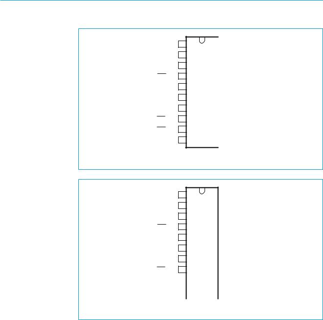
5.Pinning information
5.1Pinning
handbook, halfpage
KBI0/CMP2/P0.0 1
P1.7 2
P1.6 3
RST/P1.5 4
VSS 5
XTAL1/P3.1 6
CLKOUT/XTAL2/P3.0 7
INT1/P1.4 8
SDA/INT0/P1.3 9
SCL/T0/P1.2 10
P89LPC920FDH |
P89LPC921FDH |
P89LPC922FDH |
P89LPC9221FDH |
|
P0.1/CIN2B/KBI1 |
20 |
|
|
P0.2/CIN2A/KBI2 |
19 |
|
|
P0.3/CIN1B/KBI3 |
18 |
|
|
P0.4/CIN1A/KBI4 |
17 |
|
|
P0.5/CMPREF/KBI5 |
16 |
|
|
VDD |
15 |
|
|
P0.6/CMP1/KBI6 |
14 |
|
|
P0.7/T1/KBI7 |
13 |
|
|
P1.0/TXD |
12 |
|
|
P1.1/RXD |
11 |
|
|
|
002aaa408
Fig 2. TSSOP20 pin configuration.
handbook, halfpage
KBI0/CMP2/P0.0 1
P1.7 2
P1.6 3
RST/P1.5 4
VSS 5
XTAL1/P3.1 6
CLKOUT/XTAL2/P3.0 7
INT1/P1.4 8
P89LPC922FN |
P89LPC9221FN |
20 |
P0.1/CIN2B/KBI1 |
|
P0.2/CIN2A/KBI2 |
19 |
|
|
P0.3/CIN1B/KBI3 |
18 |
|
|
P0.4/CIN1A/KBI4 |
17 |
|
|
P0.5/CMPREF/KBI5 |
16 |
|
|
VDD |
15 |
|
|
P0.6/CMP1/KBI6 |
14 |
|
|
P0.7/T1/KBI7 |
13 |
|
|
|
9 |
|
|
|
12 |
P1.0/TXD |
|
SDA/INT0/P1.3 |
|
|
|
||||||
SCL/T0/P1.2 |
|
|
|
|
|
P1.1/RXD |
|||
10 |
|
11 |
|||||||
|
|
|
|
|
|
|
|
|
|
|
|
|
|
|
002aaa407 |
|
|||
Fig 3. DIP20 pin configuration.
9397 750 14469 |
© Koninklijke Philips Electronics N.V. 2004. All rights reserved. |
Product data |
Rev. 08 — 15 December 2004 |
5 of 46 |
Philips Semiconductors |
P89LPC920/921/922/9221 |
||||
|
|
|
|
|
8-bit microcontrollers with two-clock 80C51 core |
|
|
|
5.2 Pin description |
||
Table 3: |
Pin description |
|
|||
|
|
|
|
|
|
Symbol |
|
Pin |
|
Type |
Description |
P0.0 to P0.7 |
|
I/O |
Port 0: Port 0 is an 8-bit I/O port with a user-configurable output type. During reset |
||
|
|
|
|
|
Port 0 latches are configured in the input only mode with the internal pull-up disabled. |
|
|
|
|
|
The operation of Port 0 pins as inputs and outputs depends upon the port configuration |
|
|
|
|
|
selected. Each port pin is configured independently. Refer to Section 8.12.1 “Port |
|
|
|
|
|
configurations” and Table 8 “DC electrical characteristics” for details. |
|
|
|
|
|
The Keypad Interrupt feature operates with Port 0 pins. |
|
|
|
|
|
All pins have Schmitt triggered inputs. |
|
|
|
|
|
Port 0 also provides various special functions as described below: |
|
|
|
|
|
|
|
1 |
|
I/O |
P0.0 — Port 0 bit 0. |
|
|
|
|
|
|
|
|
|
|
|
O |
CMP2 — Comparator 2 output. |
|
|
|
|
|
|
|
|
|
|
I |
KBI0 — Keyboard input 0. |
|
|
|
|
|
|
|
20 |
|
I/O |
P0.1 — Port 0 bit 1. |
|
|
|
|
|
|
|
|
|
|
|
I |
CIN2B — Comparator 2 positive input B. |
|
|
|
|
|
|
|
|
|
|
I |
KBI1 — Keyboard input 1. |
|
|
|
|
|
|
|
19 |
|
I/O |
P0.2 — Port 0 bit 2. |
|
|
|
|
|
|
|
|
|
|
|
I |
CIN2A — Comparator 2 positive input A. |
|
|
|
|
|
|
|
|
|
|
I |
KBI2 — Keyboard input 2. |
|
|
|
|
|
|
|
18 |
|
I/O |
P0.3 — Port 0 bit 3. High current source (P89LPC9221). |
|
|
|
|
|
|
|
|
|
|
|
I |
CIN1B — Comparator 1 positive input B. |
|
|
|
|
|
|
|
|
|
|
I |
KBI3 — Keyboard input 3. |
|
|
|
|
|
|
|
17 |
|
I/O |
P0.4 — Port 0 bit 4. High current source (P89LPC9221). |
|
|
|
|
|
|
|
|
|
|
|
I |
CIN1A — Comparator 1 positive input A. |
|
|
|
|
|
|
|
|
|
|
I |
KBI4 — Keyboard input 4. |
|
|
|
|
|
|
|
16 |
|
I/O |
P0.5 — Port 0 bit 5. High current source (P89LPC9221). |
|
|
|
|
|
|
|
|
|
|
|
I |
CMPREF — Comparator reference (negative) input. |
|
|
|
|
|
|
|
|
|
|
I |
KBI5 — Keyboard input 5. |
|
|
|
|
|
|
|
14 |
|
I/O |
P0.6 — Port 0 bit 6. High current source (P89LPC9221). |
|
|
|
|
|
|
|
|
|
|
|
O |
CMP1 — Comparator 1 output. |
|
|
|
|
|
|
|
|
|
|
I |
KBI6 — Keyboard input 6. |
|
|
|
|
|
|
|
13 |
|
I/O |
P0.7 — Port 0 bit 7. High current source (P89LPC9221). |
|
|
|
|
|
|
|
|
|
|
|
I/O |
T1 — Timer/counter 1 external count input or overflow output. |
|
|
|
|
|
|
|
|
|
|
I |
KBI7 — Keyboard input 7. |
9397 750 14469 |
© Koninklijke Philips Electronics N.V. 2004. All rights reserved. |
Product data |
Rev. 08 — 15 December 2004 |
6 of 46 |

Philips Semiconductors |
|
P89LPC920/921/922/9221 |
|||
|
|
|
|
|
8-bit microcontrollers with two-clock 80C51 core |
Table 3: |
Pin description…continued |
||||
|
|
|
|
|
|
Symbol |
|
Pin |
Type |
Description |
|
P1.0 to P1.7 |
I/O, I [1] |
Port 1: Port 1 is an 8-bit I/O port with a user-configurable output type, except for three |
|||
|
|
|
|
pins as noted below. During reset Port 1 latches are configured in the input only mode |
|
|
|
|
|
with the internal pull-up disabled. The operation of the configurable Port 1 pins as inputs |
|
|
|
|
|
and outputs depends upon the port configuration selected. Each of the configurable |
|
|
|
|
|
port pins are programmed independently. Refer to Section 8.12.1 “Port configurations” |
|
|
|
|
|
and Table 8 “DC electrical characteristics” for details. P1.2 - P1.3 are open drain when |
|
|
|
|
|
used as outputs. P1.5 is input only. |
|
|
|
|
|
All pins have Schmitt triggered inputs. |
|
|
|
|
|
Port 1 also provides various special functions as described below: |
|
|
|
|
|
|
|
|
12 |
I/O |
P1.0 — Port 1 bit 0. |
||
|
|
|
|
|
|
|
|
|
O |
TXD — Transmitter output for the serial port. |
|
|
|
|
|
|
|
|
11 |
I/O |
P1.1 — Port 1 bit 1. |
||
|
|
|
|
|
|
|
|
|
I |
RXD — Receiver input for the serial port. |
|
|
|
|
|
|
|
|
10 |
I/O |
P1.2 — Port 1 bit 2 (open-drain when used as output). |
||
|
|
|
|
|
|
|
|
|
I/O |
T0 — Timer/counter 0 external count input or overflow output (open-drain when used as |
|
|
|
|
|
output). |
|
|
|
|
|
|
|
|
|
|
I/O |
SCL — I2C serial clock input/output. |
|
|
9 |
I/O |
P1.3 — Port 1 bit 3 (open-drain when used as output). |
||
|
|
|
|
|
|
|
|
|
I |
|
— External interrupt 0 input. |
|
|
|
INT0 |
||
|
|
|
|
|
|
|
|
|
I/O |
SDA — I2C serial data input/output. |
|
|
8 |
I/O |
P1.4 — Port 1 bit 4. High current source (P89LPC9221). |
||
|
|
|
|
|
|
|
|
|
I |
|
— External interrupt 1 input. |
|
|
|
INT1 |
||
4I P1.5 — Port 1 bit 5 (input only).
I RST — External Reset input (if selected via FLASH configuration). A LOW on this pin resets the microcontroller, causing I/O ports and peripherals to take on their default states, and the processor begins execution at address 0. When using an oscillator frequency above 12 MHz, the reset input function of P1.5 must be enabled. An external circuit is required to hold the device in reset at power-up until VDD has reached its specified level. When system power is removed V DD will fall below the minimum specified operating voltage. When using an oscillator frequency above 12 MHz, in some applications, an external brownout detect circuit may be required to hold the device in reset when VDD falls below the minimum specified operating voltage.
3 |
I/O |
P1.6 — |
Port 1 bit 6. High current source (P89LPC9221). |
2 |
I/O |
P1.7 — |
Port 1 bit 7. High current source (P89LPC9221). |
9397 750 14469 |
© Koninklijke Philips Electronics N.V. 2004. All rights reserved. |
Product data |
Rev. 08 — 15 December 2004 |
7 of 46 |
Philips Semiconductors |
P89LPC920/921/922/9221 |
||
|
|
|
8-bit microcontrollers with two-clock 80C51 core |
Table 3: |
Pin description…continued |
||
|
|
|
|
Symbol |
Pin |
Type |
Description |
P3.0 to P3.1 |
I/O |
Port 3: Port 3 is an 2-bit I/O port with a user-configurable output type. During reset |
|
|
|
|
Port 3 latches are configured in the input only mode with the internal pull-up disabled. |
The operation of Port 3 pins as inputs and outputs depends upon the port configuration selected. Each port pin is configured independently. Refer to Section 8.12.1 “Port configurations” and Table 8 “DC electrical characteristics” for details.
All pins have Schmitt triggered inputs.
Port 3 also provides various special functions as described below:
7I/O P3.0 — Port 3 bit 0.
O XTAL2 — Output from the oscillator amplifier (when a crystal oscillator option is selected via the FLASH configuration.
O CLKOUT — CPU clock divided by 2 when enabled via SFR bit (ENCLK - TRIM.6). It can be used if the CPU clock is the internal RC oscillator, watchdog oscillator or external clock input, except when XTAL1/XTAL2 are used to generate clock source for the real time clock/system timer.
|
6 |
I/O |
P3.1 — Port 3 bit 1. |
|
|
I |
XTAL1 — Input to the oscillator circuit and internal clock generator circuits (when |
|
|
|
selected via the FLASH configuration). It can be a port pin if internal RC oscillator or |
|
|
|
watchdog oscillator is used as the CPU clock source, and if XTAL1/XTAL2 are not used |
|
|
|
to generate the clock for the real time clock/system timer. |
|
|
|
|
VSS |
5 |
I |
Ground: 0 V reference. |
VDD |
15 |
I |
Power Supply: This is the power supply voltage for normal operation as well as Idle |
|
|
|
and Power down modes. |
|
|
|
|
[1] Input/Output for P1.0-P1.4, P1.6, P1.7. Input for P1.5.
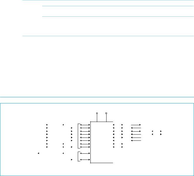
6. Logic symbol
KBI0 |
|
|
CMP2 |
|
|
|
|
|
|
|
|
||||
KBI1 |
|
|
CIN2B |
|
|
|
|
|
|
|
|
|
|||
KBI2 |
|
|
CIN2A |
|
|
||
|
|
|
0 |
||||
KBI3 |
|
|
CIN1B |
|
|
|
PORT |
|
|
|
|
|
|
||
KBI4 |
|
|
CIN1A |
|
|
|
|
|
|
|
|
|
|||
KBI5 |
|
|
CMPREF |
|
|
|
|
|
|
|
|
|
|||
KBI6 |
|
|
CMP1 |
|
|
|
|
|
|
|
|
||||
KBI7 |
|
|
T1 |
|
|
|
|
|
3 |
||||||
CLKOUT |
|
|
XTAL2 |
||||
|
|
|
|
PORT |
|||
|
|
|
XTAL1 |
|
|
|
|
|
|
|
|
||||
Fig 4. Logic symbol.
VDD VSS
P89LPC920/921/922/9221 |
|
|
|
|
|
|
PORT 1 |
|
|
|
|
|
|
||
|
|
|
|
|
|
||
|
|
|
|||||
|
|
|
|||||
|
|
|
|||||
|
|
|
|
|
|
|
|
|
|
|
|
|
|
|
|
|
|
|
|
|
|
|
|
|
|
|
|
|
|
|
|
|
|
|
|
|
|
|
|
|
002aaa409 |
||||||
TxD |
|
|
|
RxD |
|
|
|
T0 |
|
SCL |
|
|
|||
INT0 |
|
|
SDA |
|
|
||
INT1 |
|
|
|
RST |
|
|
|
9397 750 14469 |
© Koninklijke Philips Electronics N.V. 2004. All rights reserved. |
Product data |
Rev. 08 — 15 December 2004 |
8 of 46 |

Philips Semiconductors |
P89LPC920/921/922/9221 |
|
8-bit microcontrollers with two-clock 80C51 core |
7. Special function registers
Remark: Special Function Registers (SFRs) accesses are restricted in the following ways:
•User must not attempt to access any SFR locations not defined.
•Accesses to any defined SFR locations must be strictly for the functions for the SFRs.
•SFR bits labeled ‘-’, ‘0’ or ‘1’ can only be written and read as follows:
–‘-’ Unless otherwise specified, must be written with ‘0’, but can return any value when read (even if it was written with ‘0’). It is a reserved bit and may be used in future derivatives.
–‘0’ must be written with ‘0’, and will return a ‘0’ when read.
–‘1’ must be written with ‘1’, and will return a ‘1’ when read.
9397 750 14469 |
© Koninklijke Philips Electronics N.V. 2004. All rights reserved. |
Product data |
Rev. 08 — 15 December 2004 |
9 of 46 |

data Product
2004 December 15 — 08 .Rev
46 of 10
14469 750 9397
.reserved rights All .2004 .V.N Electronics Philips Koninklijke ©
Table 4: |
Special function registers |
|
|
|
|
|
|
|
|
|
|
|
* indicates SFRs that are bit addressable. |
|
|
|
|
|
|
|
|
|
|
|
|
|
|
|
|
|
|
|
|
|
|
|
||
Name |
Description |
SFR |
Bit functions and addresses |
|
|
|
|
|
Reset value |
|||
|
|
addr. |
MSB |
|
|
|
|
|
|
LSB |
Hex |
Binary |
|
|
|
|
|
|
|
|
|
||||
|
Bit address |
E7 |
E6 |
E5 |
E4 |
E3 |
E2 |
E1 |
E0 |
|
|
|
ACC* |
Accumulator |
E0H |
|
|
|
|
|
|
|
|
00 |
00000000 |
AUXR1 |
Auxiliary function register |
A2H |
CLKLP |
EBRR |
ENT1 |
ENT0 |
SRST |
0 |
- |
DPS |
00[1] |
000000x0 |
|
Bit address |
F7 |
F6 |
F5 |
F4 |
F3 |
F2 |
F1 |
F0 |
|
|
|
B* |
B register |
F0H |
|
|
|
|
|
|
|
|
00 |
00000000 |
BRGR0[2] |
Baud rate generator rate |
BEH |
|
|
|
|
|
|
|
|
00 |
00000000 |
|
LOW |
|
|
|
|
|
|
|
|
|
|
|
BRGR1[2] |
Baud rate generator rate |
BFH |
|
|
|
|
|
|
|
|
00 |
00000000 |
|
HIGH |
|
|
|
|
|
|
|
|
|
|
|
BRGCON |
Baud rate generator control |
BDH |
- |
- |
- |
- |
- |
- |
SBRGS |
BRGEN |
00 |
xxxxxx00 |
CMP1 |
Comparator 1 control register |
ACH |
- |
- |
CE1 |
CP1 |
CN1 |
OE1 |
CO1 |
CMF1 |
00[1] |
xx000000 |
CMP2 |
Comparator 2 control register |
ADH |
- |
- |
CE2 |
CP2 |
CN2 |
OE2 |
CO2 |
CMF2 |
00[1] |
xx000000 |
DIVM |
CPU clock divide-by-M |
95H |
|
|
|
|
|
|
|
|
00 |
00000000 |
|
control |
|
|
|
|
|
|
|
|
|
|
|
DPTR |
Data pointer (2 bytes) |
|
|
|
|
|
|
|
|
|
|
|
DPH |
Data pointer HIGH |
83H |
|
|
|
|
|
|
|
|
00 |
00000000 |
DPL |
Data pointer LOW |
82H |
|
|
|
|
|
|
|
|
00 |
00000000 |
FMADRH |
Program Flash address HIGH |
E7H |
|
|
|
|
|
|
|
|
00 |
00000000 |
FMADRL |
Program Flash address LOW |
E6H |
|
|
|
|
|
|
|
|
00 |
00000000 |
FMCON |
Program Flash control (Read) |
E4H |
BUSY |
- |
- |
- |
HVA |
HVE |
SV |
OI |
70 |
01110000 |
|
Program Flash control (Write) |
E4H |
FMCMD. |
FMCMD. FMCMD. FMCMD. FMCMD. FMCMD. |
FMCMD. |
FMCMD. |
|
|
||||
|
|
|
7 |
6 |
5 |
4 |
3 |
2 |
1 |
0 |
|
|
FMDATA |
Program Flash data |
E5H |
|
|
|
|
|
|
|
|
00 |
00000000 |
I2ADR |
I2C slave address register |
DBH |
I2ADR.6 |
I2ADR.5 |
I2ADR.4 |
I2ADR.3 |
I2ADR.2 |
I2ADR.1 |
I2ADR.0 |
GC |
00 |
00000000 |
|
Bit address |
DF |
DE |
DD |
DC |
DB |
DA |
D9 |
D8 |
|
|
|
I2CON* |
I2C control register |
D8H |
- |
I2EN |
STA |
STO |
SI |
AA |
- |
CRSEL |
00 |
x00000x0 |
I2DAT |
I2C data register |
DAH |
|
|
|
|
|
|
|
|
|
|
I2SCLH |
Serial clock generator/SCL |
DDH |
|
|
|
|
|
|
|
|
00 |
00000000 |
|
duty cycle register HIGH |
|
|
|
|
|
|
|
|
|
|
|
|
|
|
|
|
|
|
|
|
|
|
|
|
Semiconductors Philips
core 80C51 clock-two with microcontrollers bit-8 |
P89LPC920/921/922/9221 |
data Product
2004 December 15 — 08 .Rev
46 of 11
14469 750 9397
.reserved rights All .2004 .V.N Electronics Philips Koninklijke ©
Table 4: |
Special function registers…continued |
|
|
|
|
|
|
|
|
|
|
|
|
|
|
|
|
|
* indicates SFRs that are bit addressable. |
|
|
|
|
|
|
|
|
|
|
|
|
|
|
|
|
|
|
|
|
|
|
|
|
|
|
|
|
|
|
|
|
|
||||
Name |
Description |
SFR |
Bit functions and addresses |
|
|
|
|
|
|
|
|
|
Reset value |
|||||
|
|
addr. |
MSB |
|
|
|
|
|
|
|
|
|
|
|
|
LSB |
Hex |
Binary |
|
|
|
|
|
|
|
|
|
|
|
|
|
|
|
||||
I2SCLL |
Serial clock generator/SCL |
DCH |
|
|
|
|
|
|
|
|
|
|
|
|
|
|
00 |
00000000 |
|
duty cycle register LOW |
|
|
|
|
|
|
|
|
|
|
|
|
|
|
|
|
|
I2STAT |
I2C status register |
D9H |
STA.4 |
STA.3 |
STA.2 |
STA.1 |
STA.0 |
0 |
0 |
0 |
F8 |
11111000 |
||||||
|
Bit address |
AF |
AE |
|
AD |
|
AC |
|
AB |
AA |
A9 |
A8 |
|
|
||||
IEN0* |
Interrupt enable 0 |
A8H |
EA |
EWDRT |
EBO |
ES/ESR |
|
ET1 |
EX1 |
ET0 |
EX0 |
00[1] |
00000000 |
|||||
|
Bit address |
EF |
EE |
|
ED |
|
EC |
|
EB |
EA |
E9 |
E8 |
|
|
||||
IEN1* |
Interrupt enable 1 |
E8H |
- |
EST |
- |
|
- |
|
- |
|
EC |
EKBI |
EI2C |
00[1] |
00x00000 |
|||
|
Bit address |
BF |
BE |
|
BD |
|
BC |
|
BB |
BA |
B9 |
B8 |
|
|
||||
IP0* |
Interrupt priority 0 |
B8H |
- |
PWDRT |
PBO |
PS/PSR |
|
PT1 |
PX1 |
PT0 |
PX0 |
00[1] |
x0000000 |
|||||
IP0H |
Interrupt priority 0 HIGH |
B7H |
- |
PWDRT |
PBOH |
PSH/ |
PT1H |
PX1H |
PT0H |
PX0H |
00[1] |
x0000000 |
||||||
|
|
|
|
H |
|
|
|
PSRH |
|
|
|
|
|
|
|
|
||
|
Bit address |
FF |
FE |
|
FD |
|
FC |
|
FB |
FA |
F9 |
F8 |
|
|
||||
IP1* |
Interrupt priority 1 |
F8H |
- |
PST |
- |
|
- |
|
- |
|
PC |
PKBI |
PI2C |
00[1] |
00x00000 |
|||
IP1H |
Interrupt priority 1 HIGH |
F7H |
- |
PSTH |
- |
|
- |
|
- |
|
PCH |
PKBIH |
PI2CH |
00[1] |
00x00000 |
|||
KBCON |
Keypad control register |
94H |
- |
- |
- |
|
- |
|
- |
|
- |
PATN |
KBIF |
00[1] |
xxxxxx00 |
|||
|
|
|
|
|
|
|
|
|
|
|
|
|
|
|
_SEL |
|
|
|
KBMASK |
Keypad interrupt mask |
86H |
|
|
|
|
|
|
|
|
|
|
|
|
|
|
00 |
00000000 |
|
register |
|
|
|
|
|
|
|
|
|
|
|
|
|
|
|
|
|
KBPATN |
Keypad pattern register |
93H |
|
|
|
|
|
|
|
|
|
|
|
|
|
|
FF |
11111111 |
|
Bit address |
87 |
86 |
85 |
|
84 |
|
83 |
|
82 |
81 |
80 |
|
|
||||
P0* |
Port 0 |
80H |
T1/KB7 |
CMP1 |
CMPREF |
CIN1A |
CIN1B |
CIN2A |
CIN2B |
CMP2 |
|
[1] |
||||||
|
|
|
|
/KB6 |
/KB5 |
/KB4 |
|
/KB3 |
/KB2 |
/KB1 |
/KB0 |
|
|
|||||
|
Bit address |
97 |
96 |
95 |
|
94 |
|
93 |
|
92 |
91 |
90 |
|
|
||||
P1* |
Port 1 |
90H |
- |
- |
|
|
|
|
|
|
|
|
|
T0/SCL |
RXD |
TXD |
|
[1] |
|
RST |
INT1 |
INT0/ |
|
||||||||||||||
|
|
|
|
|
|
|
|
|
|
|
|
SDA |
|
|
|
|
|
|
|
Bit address |
B7 |
B6 |
|
B5 |
|
B4 |
|
B3 |
B2 |
B1 |
B0 |
|
|
||||
P3* |
Port 3 |
B0H |
- |
- |
- |
|
- |
|
- |
|
- |
XTAL1 |
XTAL2 |
|
[1] |
|||
P0M1 |
Port 0 output mode 1 |
84H |
(P0M1.7) |
(P0M1.6) |
(P0M1.5) |
(P0M1.4) |
(P0M1.3) |
(P0M1.2) |
(P0M1.1) |
(P0M1.0) |
FF |
11111111 |
||||||
P0M2 |
Port 0 output mode 2 |
85H |
(P0M2.7) |
(P0M2.6) |
(P0M2.5) |
(P0M2.4) |
(P0M2.3) |
(P0M2.2) |
(P0M2.1) |
(P0M2.0) |
00 |
00000000 |
||||||
P1M1 |
Port 1 output mode 1 |
91H |
(P1M1.7) |
(P1M1.6) |
- |
|
(P1M1.4) |
(P1M1.3) |
(P1M1.2) |
(P1M1.1) |
(P1M1.0) |
D3[1] |
11x1xx11 |
|||||
Semiconductors Philips
core 80C51 clock-two with microcontrollers bit-8 |
P89LPC920/921/922/9221 |

data Product
2004 December 15 — 08 .Rev
46 of 12
14469 750 9397
.reserved rights All .2004 .V.N Electronics Philips Koninklijke ©
Table 4: |
Special function registers…continued |
|
|
|
|
|
|
|
|
|
|
|
* indicates SFRs that are bit addressable. |
|
|
|
|
|
|
|
|
|
|
|
|
|
|
|
|
|
|
|
|
|
|
|
||
Name |
Description |
SFR |
Bit functions and addresses |
|
|
|
|
|
Reset value |
|||
|
|
addr. |
MSB |
|
|
|
|
|
|
LSB |
Hex |
Binary |
|
|
|
|
|
|
|
|
|
||||
P1M2 |
Port 1 output mode 2 |
92H |
(P1M2.7) |
(P1M2.6) |
- |
(P1M2.4) |
(P1M2.3) |
(P1M2.2) |
(P1M2.1) |
(P1M2.0) |
00[1] |
00x0xx00 |
P3M1 |
Port 3 output mode 1 |
B1H |
- |
- |
- |
- |
- |
- |
(P3M1.1) |
(P3M1.0) |
03[1] |
xxxxxx11 |
P3M2 |
Port 3 output mode 2 |
B2H |
- |
- |
- |
- |
- |
- |
(P3M2.1) |
(P3M2.0) |
00[1] |
xxxxxx00 |
PCON |
Power control register |
87H |
SMOD1 |
SMOD0 |
BOPD |
BOI |
GF1 |
GF0 |
PMOD1 |
PMOD0 |
00 |
00000000 |
PCONA |
Power control register A |
B5H |
RTCPD |
- |
VCPD |
- |
I2PD |
- |
SPD |
- |
00[1] |
00000000 |
|
Bit address |
D7 |
D6 |
D5 |
D4 |
D3 |
D2 |
D1 |
D0 |
|
|
|
PSW* |
Program status word |
D0H |
CY |
AC |
F0 |
RS1 |
RS0 |
OV |
F1 |
P |
00H |
00000000 |
PT0AD |
Port 0 digital input disable |
F6H |
- |
- |
PT0AD.5 |
PT0AD.4 |
PT0AD.3 |
PT0AD.2 |
PT0AD.1 |
- |
00H |
xx00000x |
RSTSRC |
Reset source register |
DFH |
- |
- |
BOF |
POF |
R_BK |
R_WD |
R_SF |
R_EX |
|
[3] |
RTCCON |
Real-time clock control |
D1H |
RTCF |
RTCS1 |
RTCS0 |
- |
- |
- |
ERTC |
RTCEN |
60[1][6] |
|
RTCH |
Real-time clock register |
D2H |
|
|
|
|
|
|
|
|
00[6] |
00000000 |
|
HIGH |
|
|
|
|
|
|
|
|
|
|
|
RTCL |
Real-time clock register LOW |
D3H |
|
|
|
|
|
|
|
|
00[6] |
00000000 |
SADDR |
Serial port address register |
A9H |
|
|
|
|
|
|
|
|
00 |
00000000 |
SADEN |
Serial port address enable |
B9H |
|
|
|
|
|
|
|
|
00 |
00000000 |
SBUF |
Serial Port data buffer |
99H |
|
|
|
|
|
|
|
|
xx |
xxxxxxxx |
|
register |
|
|
|
|
|
|
|
|
|
|
|
|
Bit address |
9F |
9E |
9D |
9C |
9B |
9A |
99 |
98 |
|
|
|
SCON* |
Serial port control |
98H |
SM0/FE |
SM1 |
SM2 |
REN |
TB8 |
RB8 |
TI |
RI |
00 |
00000000 |
SSTAT |
Serial port extended status |
BAH |
DBMOD |
INTLO |
CIDIS |
DBISEL |
FE |
BR |
OE |
STINT |
00 |
00000000 |
|
register |
|
|
|
|
|
|
|
|
|
|
|
SP |
Stack pointer |
81H |
|
|
|
|
|
|
|
|
07 |
00000111 |
TAMOD |
Timer 0 and 1 auxiliary mode |
8FH |
- |
- |
- |
T1M2 |
- |
- |
- |
T0M2 |
00 |
xxx0xxx0 |
|
Bit address |
8F |
8E |
8D |
8C |
8B |
8A |
89 |
88 |
|
|
|
TCON* |
Timer 0 and 1 control |
88H |
TF1 |
TR1 |
TF0 |
TR0 |
IE1 |
IT1 |
IE0 |
IT0 |
00 |
00000000 |
TH0 |
Timer 0 HIGH |
8CH |
|
|
|
|
|
|
|
|
00 |
00000000 |
TH1 |
Timer 1 HIGH |
8DH |
|
|
|
|
|
|
|
|
00 |
00000000 |
TL0 |
Timer 0 LOW |
8AH |
|
|
|
|
|
|
|
|
00 |
00000000 |
TL1 |
Timer 1 LOW |
8BH |
|
|
|
|
|
|
|
|
00 |
00000000 |
TMOD |
Timer 0 and 1 mode |
89H |
T1GATE |
T1C/T |
T1M1 |
T1M0 |
T0GATE |
T0C/T |
T0M1 |
T0M0 |
00 |
00000000 |
|
|
|
|
|
|
|
|
|
|
|
|
|
Semiconductors Philips
core 80C51 clock-two with microcontrollers bit-8 |
P89LPC920/921/922/9221 |

data Product
2004 December 15 — 08 .Rev
46 of 13
14469 750 9397
.reserved rights All .2004 .V.N Electronics Philips Koninklijke ©
Table 4: |
Special function registers…continued |
|
|
|
|
|
|
|
|
|
|
|
|
* indicates SFRs that are bit addressable. |
|
|
|
|
|
|
|
|
|
|
|
|
|
|
|
|
|
|
|
|
|
|
|
|
|||
Name |
Description |
SFR |
Bit functions and addresses |
|
|
|
|
|
Reset value |
||||
|
|
addr. |
MSB |
|
|
|
|
|
|
LSB |
Hex |
|
Binary |
|
|
|
|
|
|
|
|
|
|
||||
TRIM |
Internal oscillator trim register |
96H |
- |
ENCLK |
TRIM.5 |
TRIM.4 |
TRIM.3 |
TRIM.2 |
TRIM.1 |
TRIM.0 |
|
[5] [6] |
|
WDCON |
Watchdog control register |
A7H |
PRE2 |
PRE1 |
PRE0 |
- |
- |
WDRUN |
WDTOF |
WDCLK |
|
[4] [6] |
|
WDL |
Watchdog load |
C1H |
|
|
|
|
|
|
|
|
FF |
11111111 |
|
WFEED1 |
Watchdog feed 1 |
C2H |
|
|
|
|
|
|
|
|
|
|
|
WFEED2 |
Watchdog feed 2 |
C3H |
|
|
|
|
|
|
|
|
|
|
|
|
|
|
|
|
|
|
|
|
|
|
|
|
|
[1]All ports are in input only (high impedance) state after power-up.
[2]BRGR1 and BRGR0 must only be written if BRGEN in BRGCON SFR is ‘0’. If any are written while BRGEN = 1, the result is unpredictable.
[3]The RSTSRC register reflects the cause of the P89LPC920/921/922/9221 reset. Upon a power-up reset, all reset source flags are cleared except POF and BOF; the power-on reset value is xx110000.
[4]After reset, the value is 111001x1, i.e., PRE2-PRE0 are all ‘1’, WDRUN = 1 and WDCLK = 1. WDTOF bit is ‘1’ after watchdog reset and is ‘0’ after power-on reset. Other resets will not affect WDTOF.
[5]On power-on reset, the TRIM SFR is initialized with a factory preprogrammed value. Other resets will not cause initialization of the TRIM register.
[6]The only reset source that affects these SFRs is power-on reset.
Semiconductors Philips
core 80C51 clock-two with microcontrollers bit-8 |
P89LPC920/921/922/9221 |

Philips Semiconductors |
P89LPC920/921/922/9221 |
|
8-bit microcontrollers with two-clock 80C51 core |
8. Functional description
Remark: Please refer to the P89LPC920/921/922/9221 User’s Manual for a more detailed functional description.
8.1 Enhanced CPU
The P89LPC920/921/922/9221 uses an enhanced 80C51 CPU which runs at 6 times the speed of standard 80C51 devices. A machine cycle consists of two CPU clock cycles, and most instructions execute in one or two machine cycles.
8.2 Clocks
8.2.1Clock definitions
The P89LPC920/921/922/9221 device has several internal clocks as defined below:
OSCCLK — Input to the DIVM clock divider. OSCCLK is selected from one of four clock sources (see Figure 5) and can also be optionally divided to a slower frequency (see Section 8.7 “CPU Clock (CCLK) modification: DIVM register”).
Note: fosc is defined as the OSCCLK frequency.
CCLK — CPU clock; output of the clock divider. There are two CCLK cycles per machine cycle, and most instructions are executed in one to two machine cycles (two or four CCLK cycles).
RCCLK — The internal 7.373 MHz RC oscillator output.
PCLK — Clock for the various peripheral devices and is CCLK/2
8.2.2CPU clock (OSCCLK)
The P89LPC920/921/922/9221 provides several user-selectable oscillator options in generating the CPU clock. This allows optimization for a range of needs from high precision to lowest possible cost. These options are configured when the FLASH is programmed and include an on-chip watchdog oscillator, an on-chip RC oscillator, an oscillator using an external crystal, or an external clock source. The crystal oscillator can be optimized for low, medium, or high frequency crystals covering a range from 20 kHz to 12 MHz.
8.2.3Low speed oscillator option
This option supports an external crystal in the range of 20 kHz to 100 kHz. Ceramic resonators are also supported in this configuration.
8.2.4Medium speed oscillator option
This option supports an external crystal in the range of 100 kHz to 4 MHz. Ceramic resonators are also supported in this configuration.
8.2.5High speed oscillator option
This option supports an external crystal in the range of 4 MHz to 18 MHz. Ceramic resonators are also supported in this configuration. When using an oscillator frequency above 12 MHz, the reset input function of P1.5 must be enabled. An
external circuit is required to hold the device in reset at power-up until VDD has reached its specified level. When system power is removed V DD will fall below
9397 750 14469 |
© Koninklijke Philips Electronics N.V. 2004. All rights reserved. |
Product data |
Rev. 08 — 15 December 2004 |
14 of 46 |
Loading...