


INTEGRATED CIRCUITS
DATA SHEET
74AHC373; 74AHCT373
Octal D-type transparent latch; 3-state
Product specification |
1999 Nov 23 |
Supersedes data of 1998 Dec 11
File under Integrated Circuits, IC06

Philips Semiconductors |
Product specification |
|
|
Octal D-type transparent latch; 3-state |
74AHC373; 74AHCT373 |
|
|
|
|
FEATURES
·ESD protection:
HBM EIA/JESD22-A114-A exceeds 2000 V MM EIA/JESD22-A115-A exceeds 200 V CDM EIA/JESD22-C101 exceeds 1000 V
·Balanced propagation delays
·All inputs have Schmitt-trigger actions
·Inputs accepts voltages higher than VCC
·Common 3-state output enable input
·Functionally identical to the ‘533’, ‘563’ and ‘573’
·For AHC only: operates with CMOS input levels
·For AHCT only: operates with TTL input levels
·Specified from -40 to +85 °C and -40 to +125 °C.
DESCRIPTION
The 74AHC/AHCT373 are high-speed Si-gate CMOS devices and are pin compatible with Low power Schottky TTL (LSTTL). They are specified in compliance with JEDEC standard no. 7A.
QUICK REFERENCE DATA
Ground = 0 V; Tamb = 25 °C; tr = tf £ 3.0 ns.
The 74AHC/AHCT373 are octal D-type transparent latches featuring separate D-type inputs for each latch and 3-state outputs for bus oriented applications. A Latch Enable (LE) input and an Output Enable (OE) input are common to all latches.
The ‘373’ consists of eight D-type transparent latches with 3-state true outputs. When LE is HIGH, data at the
Dn inputs enters the latches. In this condition the latches are transparent, i.e. a latch output will change state each time its corresponding D-input changes.
When LE is LOW the latches store the information that was present at the D-inputs a set-up time preceding the HIGH-to-LOW transition of LE. When OE is LOW, the contents of the 8 latches are available at the outputs. When OE is HIGH, the outputs go to the high-impedance OFF-state. Operation of the OE input does not affect the state of the latches.
The ‘373’ is functionally identical to the ‘533’, ‘563’ and ‘573’, but the ‘533’ and ‘563’ have inverted outputs and the ‘563’ and ‘573’ have a different pin arrangement.
SYMBOL |
PARAMETER |
CONDITIONS |
|
TYPICAL |
UNIT |
|
|
|
|
||||
AHC |
|
AHCT |
||||
|
|
|
|
|
||
|
|
|
|
|
|
|
tPHL/tPLH |
propagation delay |
CL = 15 pF; VCC = 5 V |
4.3 |
|
4.3 |
ns |
|
Dn to Qn; LE to Qn |
|
|
|
|
|
CI |
input capacitance |
VI = VCC or GND |
3.0 |
|
3.0 |
pF |
CO |
output capacitance |
|
4.0 |
|
4.0 |
pF |
CPD |
power dissipation |
CL = 50 pF; f = 1 MHz; |
10 |
|
12 |
pF |
|
capacitance |
notes 1 and 2 |
|
|
|
|
|
|
|
|
|
|
|
Notes
1.CPD is used to determine the dynamic power dissipation (PD in mW). PD = CPD ´ VCC2 ´ fi + å (CL ´ VCC2 ´ fo) where:
fi = input frequency in MHz; fo = output frequency in MHz;
å (CL ´ VCC2 ´ fo) = sum of outputs;
CL = output load capacitance in pF;
VCC = supply voltage in Volts.
2. The condition is VI = GND to VCC.
1999 Nov 23 |
2 |

Philips Semiconductors |
|
|
|
|
|
|
|
Product specification |
|
|
|
|
|
|
|
|
|
||
Octal D-type transparent latch; 3-state |
|
74AHC373; 74AHCT373 |
|||||||
|
|
|
|
|
|
|
|
|
|
FUNCTION TABLE |
|
|
|
|
|
|
|
|
|
See note 1. |
|
|
|
|
|
|
|
|
|
|
|
|
|
|
|
|
|
|
|
OPERATING MODES |
|
|
|
INPUTS |
|
|
INTERNAL |
|
OUTPUTS |
|
|
|
|
|
|
|
|
||
|
|
|
|
|
|
LATCHES |
|
|
|
|
OE |
|
LE |
Dn |
|
|
Q0 to Q7 |
||
|
|
|
|
|
|||||
Enable and read register |
|
L |
|
H |
L |
|
L |
|
L |
(transparent mode) |
|
|
|
|
|
|
|
|
|
|
L |
|
H |
H |
|
H |
|
H |
|
|
|
|
|
|
|||||
|
|
|
|
|
|
|
|
|
|
Latch and read register |
|
L |
|
L |
I |
|
L |
|
L |
|
|
|
|
|
|
|
|
|
|
|
|
L |
|
L |
h |
|
H |
|
H |
|
|
|
|
|
|
|
|
|
|
Latch register and |
|
H |
|
X |
X |
|
X |
|
Z |
disable outputs |
|
|
|
|
|
|
|
|
|
|
H |
|
X |
X |
|
X |
|
Z |
|
|
|
|
|
|
|||||
|
|
|
|
|
|
|
|
|
|
Note
1.H = HIGH voltage level;
h = HIGH voltage level one set-up time prior to the HIGH-to-LOW LE transition; L = LOW voltage level;
I = LOW voltage level one set-up time prior to the HIGH-to-LOW LE transition; X = don’t care;
Z = high-impedance OFF-state.
ORDERING INFORMATION
OUTSIDE NORTH |
|
NORTH AMERICA |
|
PACKAGES |
|
|||
|
|
|
|
|
|
|||
AMERICA |
|
PINS |
PACKAGE |
|
MATERIAL |
CODE |
||
|
|
|
|
|||||
|
|
|
|
|
||||
|
|
|
|
|
|
|
||
74AHC373D |
74AHC373D |
20 |
SO |
|
plastic |
SOT163-1 |
||
|
|
|
|
|
|
|
|
|
74AHC373PW |
|
74AHC373PW DH |
20 |
TSSOP |
|
plastic |
SOT360-1 |
|
|
|
|
|
|
|
|
|
|
74AHCT373D |
|
74AHCT373D |
20 |
SO |
|
plastic |
SOT163-1 |
|
|
|
|
|
|
|
|
|
|
74AHCT373PW |
|
7AHCT373PW DH |
20 |
TSSOP |
|
plastic |
SOT360-1 |
|
|
|
|
|
|
|
|
|
|
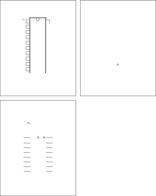
PINNING |
|
|
|
|
|
|
|
|
|
|
|
|
|
|
|
||
PIN |
|
|
SYMBOL |
|
DESCRIPTION |
|
||
|
|
|
|
|
|
|
||
1 |
|
|
|
output enable input (active LOW) |
|
|
||
OE |
|
|
||||||
2, 5, 6, 9, 12, 15, 16 |
Q0 to Q7 |
latch outputs |
|
|
|
|
||
and 19 |
|
|
|
|
|
|
|
|
|
|
|
|
|
|
|
||
3, 4, 7, 8, 13, 14, 17 |
D0 to D7 |
data inputs |
|
|
|
|
||
and 18 |
|
|
|
|
|
|
|
|
|
|
|
|
|
|
|
||
10 |
GND |
ground (0 V) |
|
|
|
|
||
|
|
|
|
|
||||
11 |
LE |
latch enable input (active HIGH) |
|
|
||||
|
|
|
|
|
||||
20 |
VCC |
DC supply voltage |
|
|
||||
1999 Nov 23 |
3 |
Philips Semiconductors |
Product specification |
|
|
Octal D-type transparent latch; 3-state |
74AHC373; 74AHCT373 |
|
|
handbook, halfpage
OE |
1 |
|
|
20 |
VCC |
|
|
|
|
|
|
|
|
|
|
Q0 |
|
|
|
|
Q7 |
handbook, halfpage |
|
|
|
11 |
|
|
|||
|
|
|
|
|
|
|
|
||||||||
2 |
|
|
19 |
|
|
|
|||||||||
|
|
|
|
|
|
|
|
|
|
|
|||||
D0 |
|
|
|
|
D7 |
|
3 |
|
LE |
2 |
|
||||
3 |
|
|
18 |
D0 |
|
|
|
Q0 |
|
||||||
|
|
|
4 |
|
|
|
5 |
|
|||||||
|
|
|
|
|
|||||||||||
D1 |
|
|
|
|
D6 |
D1 |
|
|
|
Q1 |
|
||||
4 |
|
|
17 |
7 |
|
|
|
6 |
|
||||||
Q1 |
|
|
|
|
Q6 |
D2 |
|
|
|
Q2 |
|
||||
|
|
|
|
|
|
|
|
|
|
|
|||||
5 |
|
|
16 |
|
8 |
9 |
|
||||||||
|
|
D3 |
|
|
|
Q3 |
|
||||||||
Q2 |
373 |
|
|
Q5 |
|
13 |
|
|
|
12 |
|
||||
6 |
|
|
15 |
D4 |
|
|
|
Q4 |
|
||||||
|
|
|
14 |
|
|
|
15 |
|
|||||||
|
|
|
|
|
|
D5 |
D5 |
|
|
|
Q5 |
|
|||
D2 7 |
|
14 |
|
17 |
|
|
|
16 |
|
||||||
|
|
|
D6 |
|
|
|
Q6 |
||||||||
|
|
8 |
|
|
|
D4 |
18 |
|
|
|
19 |
|
|||
D |
3 |
|
|
13 |
|
||||||||||
|
|
D7 |
|
|
|
Q7 |
|
||||||||
|
|
|
|
|
|
|
|
|
|
|
|
|
|||
|
|
|
|
|
|
|
|
|
|
||||||
|
|
|
|
|
|
|
|
|
|
|
|
|
|||
Q3 |
9 |
|
|
|
Q4 |
|
|
|
OE |
|
|
||||
|
|
12 |
|
|
|
|
|
||||||||
|
|
|
|
|
|
|
1 |
MNA186 |
|||||||
|
|
|
|
|
|
|
|
|
|
|
|
||||
GND 10 |
11 |
LE |
|
|
|
|
|
|
|
|
|
||||
|
|
|
|
|
|
|
|
|
|
|
|
|
|
|
|
|
|
|
MNA185 |
|
|
|
|
|
|
|
|
|
|
|
|
Fig.1 Pin configuration. |
Fig.2 Logic symbol. |
handbook, halfpage |
1 |
EN |
|
|
|
|
|
11 |
|
|
|
||
|
C1 |
|
|
|
||
|
3 |
|
|
2 |
||
|
|
|
|
|||
|
|
|
|
|
||
|
1D |
|
||||
|
|
|
|
|
||
|
4 |
|
|
|
|
5 |
|
|
|
|
|
||
|
7 |
|
|
|
|
6 |
|
|
|
|
|
||
|
8 |
|
|
|
|
9 |
|
|
|
|
|
||
|
13 |
|
|
|
|
12 |
|
|
|
|
|
||
|
14 |
|
|
|
|
15 |
|
|
|
|
|
||
|
17 |
|
|
|
|
16 |
|
|
|
|
|
||
|
18 |
|
|
|
|
19 |
|
|
|
|
|
||
|
|
|
|
|
|
|
|
|
|
|
MNA187 |
||
Fig.3 IEC logic symbol.
1999 Nov 23 |
4 |

Philips Semiconductors |
Product specification |
|
|
Octal D-type transparent latch; 3-state |
74AHC373; 74AHCT373 |
|
|
handbook, halfpage |
|
|
|
|
|
|
|
3 |
D0 |
|
|
Q0 |
2 |
|
|
4 |
D1 |
|
|
Q1 |
5 |
|
|
7 |
D2 |
|
|
Q2 |
6 |
|
LE |
|
D3 |
|
|
Q3 |
handbook, halfpage |
|
|
8 |
LATCH |
3-STATE |
9 |
|
|
||
13 |
D4 |
Q4 |
12 |
|
|
||
1 to 8 |
OUTPUTS |
|
|
||||
14 |
D5 |
|
|
Q5 |
15 |
LE |
|
17 |
D6 |
|
|
Q6 |
16 |
|
|
|
|
|
LE |
||||
|
D7 |
|
|
Q7 |
|
|
|
18 |
|
|
19 |
|
|
||
|
|
|
|
|
D |
|
Q |
11 |
LE |
|
|
|
|
LE |
MNA189 |
|
|
|
|
|
|
||
1 |
OE |
|
|
|
|
|
|
|
|
|
|
|
|
||
|
|
|
|
MNA184 |
|
|
|
Fig.4 Functional diagram. |
Fig.5 Logic diagram (one latch). |
D0 |
D1 |
D2 |
D3 |
D4 |
D5 |
D6 |
|
D7 |
|
D Q |
D Q |
D Q |
D Q |
D Q |
D Q |
D Q |
D Q |
|
LATCH |
LATCH |
LATCH |
LATCH |
LATCH |
LATCH |
LATCH |
LATCH |
|
1 |
2 |
3 |
4 |
5 |
6 |
7 |
8 |
|
LE LE |
LE LE |
LE LE |
LE LE |
LE LE |
LE LE |
LE LE |
LE LE |
LE |
|
|
|
|
|
|
|
|
OE |
|
|
|
|
|
|
|
|
|
Q0 |
Q1 |
Q2 |
Q3 |
Q4 |
Q5 |
Q6 |
Q7 |
|
|
|
|
|
|
|
|
MNA199 |
|
|
|
Fig.6 |
Logic diagram. |
|
|
|
|
1999 Nov 23 |
|
|
|
5 |
|
|
|
|

Philips Semiconductors |
|
|
|
|
|
|
Product specification |
|||||
|
|
|
|
|
|
|
|
|
|
|||
Octal D-type transparent latch; 3-state |
|
74AHC373; 74AHCT373 |
||||||||||
|
|
|
|
|
|
|
|
|
|
|
|
|
RECOMMENDED OPERATING CONDITIONS |
|
|
|
|
|
|
|
|
|
|
||
|
|
|
|
|
|
|
|
|
|
|
|
|
SYMBOL |
PARAMETER |
|
CONDITIONS |
|
74AHC |
|
|
74AHCT |
|
UNIT |
||
|
|
|
|
|
|
|
|
|
||||
|
MIN. |
TYP. |
MAX. |
MIN. |
|
TYP. |
|
MAX. |
||||
|
|
|
|
|
|
|
||||||
|
|
|
|
|
|
|
|
|
|
|
|
|
VCC |
DC supply voltage |
|
|
2.0 |
5.0 |
5.5 |
4.5 |
|
5.0 |
|
5.5 |
V |
VI |
input voltage |
|
|
0 |
− |
5.5 |
0 |
|
− |
|
5.5 |
V |
VO |
output voltage |
|
|
0 |
− |
VCC |
0 |
|
− |
|
VCC |
V |
Tamb |
operating ambient temperature |
|
see DC and AC |
−40 |
+25 |
+85 |
−40 |
|
+25 |
|
+85 |
°C |
|
|
|
characteristics per |
−40 |
+25 |
+125 |
−40 |
|
+25 |
|
+125 |
°C |
|
|
|
device |
|
|
|
|
|
|
|
|
|
tr,tf ( t/ f) |
input rise and fall rates |
|
VCC = 3.3 ±0.3 V |
− |
− |
100 |
− |
|
− |
|
− |
ns/V |
|
|
|
VCC = 5 ±0.5 V |
− |
− |
20 |
− |
|
− |
|
20 |
ns/V |
LIMITING VALUES
In accordance with the Absolute Maximum Rating System (IEC 134); voltages are referenced to GND (ground = 0 V).
SYMBOL |
PARAMETER |
CONDITIONS |
MIN. |
MAX. |
UNIT |
|
|
|
|
|
|
VCC |
DC supply voltage |
|
−0.5 |
+7.0 |
V |
VI |
input voltage |
|
−0.5 |
+7.0 |
V |
IIK |
DC input diode current |
VI < −0.5 V; note 1 |
− |
−20 |
mA |
IOK |
DC output diode current |
VO < −0.5 V or VO > VCC + 0.5 V; note 1 |
− |
±20 |
mA |
IO |
DC output source or sink current |
−0.5 V < VO < VCC + 0.5 V |
− |
±25 |
mA |
ICC |
DC VCC or GND current |
|
− |
±75 |
mA |
Tstg |
storage temperature |
|
−65 |
+150 |
°C |
PD |
power dissipation per package |
for temperature range: −40 to +125 °C; note 2 |
− |
500 |
mW |
Notes
1.The input and output voltage ratings may be exceeded if the input and output current ratings are observed.
2.For SO package: above 70 °C the value of PD derates linearly with 8 mW/K.
For TSSOP package: above 60 °C the value of PD derates linearly with 5.5 mW/K.
1999 Nov 23 |
6 |
 Loading...