

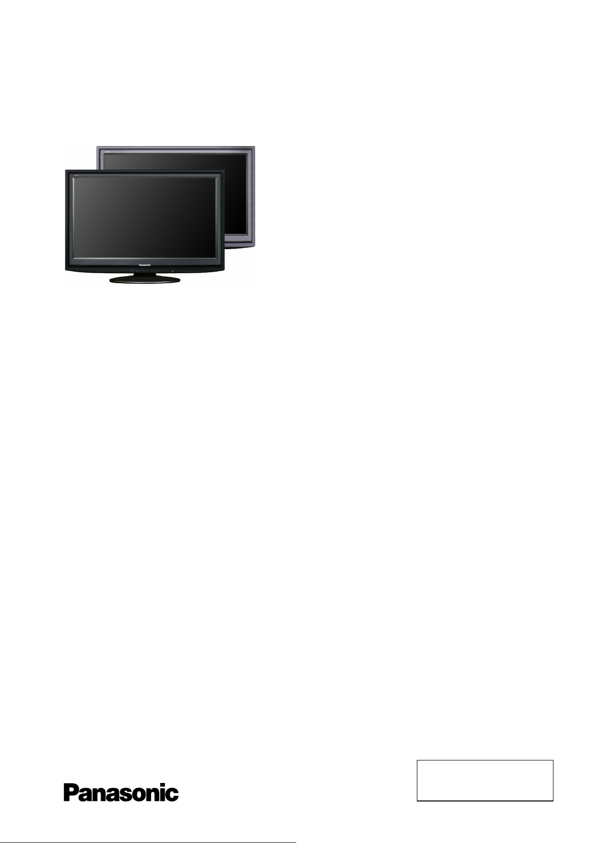
Panasonic TX-L37D25B, TX-L32D26B, TX-L32D25B Service manual
ORDER No. PCZ1004050CE
REVISION 3
Service Manual
Colour LCD Television
TX-L37D25B
TX-L32D26B
TX-L32D25B
LA02 Chassis
Specifications
(Information in brackets [ ] refers to model 32”)
Power Source: 220-240V AC, 50/60Hz
Power Consumption 147W [136W]
Stand-by Power Consumption: 0.30W (Without monitor out recording)
36W (With monitor out recording)
Aerial Impedance: 75Ω unbalanced, Coaxial Type
Receiving System: PAL-I
PAL-525/60 (AV only)
DVB-T/T2 Digital terrestrial services via UHF aerial input.
DVB-S/S2 – (freesat Other Sat.):
freesat services via Satellite dish input.
Receiver frequency range – 950 MHz to 2,150MHz
LNB Power and Polarisation – Vertical: +13V
Horizontal: +18V
Current: Max. 500mA (overload protection)
22 kHz Tone – Frequency: 22kHz ± 2kHz
Amplitude: 0.6V ± 0.2V
Symbol Rate – Max. 30MS/s
FEC Mode – 1/2, 3/5, 2/3, 3/4, 4/5, 5/6, 8/9, 9/10
Demodulation – QPSK, 8PSK
Not available for DiSEqC control.
M.NTSC (AV only)
NTSC (AV only)
PC signals: VGA, SVGA, WVGA, XGA, SXGA, WXGA (compressed)
Receiving Chanels: UHF E21-E68
Aerial - Rear:
UHF
Horizontal scanning frequency 31 – 69 kHz
Vertical scanning frequency 59 – 86 Hz
Operating Conditions: Temperature: 0°C ÷ 35°C
Humidity: 20% ÷ 80% RH (non condensing)
© Panasonic Corporation 2010.
Unauthorized copying
distribution is a violation of law.
and

Intermediate Frequency:
Video/Audio
Video 38.9MHz
Audio 32.90MHz
32.35MHz(NICAM)
Colour 34.47MHz
Terminals:
AV1 IN Video (21 pin) 1V p-p 75Ω
Audio (21 pin) 500mV rms 10kΩ
RGB (21 pin) 0.7V p-p 75Ω
AV1 OUT Video (21 pin) 1V p-p 75Ω
Audio (21 pin) 500mV rms 1kΩ
AV2 IN Video (21 pin) 1V p-p 75Ω
Audio (21 pin) 500mV rms 10kΩ
RGB (21 pin) 0.7V p-p 75Ω
S-video IN (21-pin) Y: 1V p-p 75Ω
C:0.3V p-p 75Ω
AV2 OUT Video (21 pin) 1V p-p 75Ω
Audio (21 pin) 500mV rms 1kΩ
AV3 IN Audio (RCAx2) 500mV rms 10kΩ(used for HDMI4, AV3-AUDIO)
Video (RCAx1) Y:1V p-p 75Ω
HDMI1, HDMI2, HDMI3, HDMI4 Type A Connectors
HDMI
1/3/4 :HDMI (Version 1.3a with Deep Colour)
:HDMI (Version 1.4 with Content Type)
HDMI 2 :HDMI (Version 1.4 with Content Type, Audio Return Channel)
:HDMI (Version 1.3a with Deep Colour)
This TV supports “HDAVI Control 5” function.
COMPONENT Video (RCAx3) Y:1V p-p 75Ω (including synchronization)
Pb, Pr: ±0.35V p-p 75Ω
AUDIO IN Audio (RCAx2) 500mV rms 10kΩ (used for HDMI1/2/3, COMPONENT-AUDIO)
AUDIO OUT Audio (RCAx2) 500mV rms 1kΩ (high impedance)
DIGITAL AUDIO OUT PCM / Dolby digital, Fiber optic
USB 1/2 USB 2.0 DC 5V Max 500mA
CARD SLOT SD Card slot x1
Common Interface slot x1
PC HIGH-DENSITY D_SUB 15PIN R,G,B: 700mV p-p 75Ω
HD,VD/TTL Level 2-5V p-p (high impedance)
ETHERNET RJ45, IEEE802.3 10BASE-T / 100BASE-TX
LCD screen: L5EDD9T00030 [L5EDD8T00018]
1,920 x 1,080 XGA, 16:9
Visible Diagonal 940mm [800mm]
Audio Output: 20W (2x10W), 10% THD
Headphones: 3,5mm, 8Ω Impedance
Accessories supplied : Remote Control 2 x R6 (UM3) Batteries
Dimensions:
Height: Width: Depth:
Including TV stand 632mm 917mm 287mm
[564mm 795mm 217mm]
TV set only 590mm 917mm 77mm
[521mm 795mm 77mm]
Mass:
Including TV stand 17.5kg [14.0kg]
TV set only 14.5kg [12kg]
Specifications are subject to change without notice.
Mass and dimensions shown are approximate.
Warning
This service information is designed for experienced repair technicians only and is not designed for use by the general public. It does not
contain warnings or cautions to advise non-technical individuals of potencial dangers in attempting to service a product. Products
powered by electricity should be serviced or repaired only by experienced professional technicians. Any attempt to service or repair the
product or products deal within this service information by anyone else could result in serious injury or death.
2

CONTENTS
SAFETY PRECAUTIONS........................................... 4
GENERAL GUIDE LINES...................................... 4
TOUCH – CURRENT CHECK............................... 4
PREVENTION OF ELECTROSTATIC DISCHARGE
(ESD) TO ELECTROSTATICALLY SENSITIVE (ES)
DEVICES.................................................................... 5
ABOUT LEAD FREE SOLDER (PBF)......................... 6
SUGGESTED PB FREE SOLDER........................ 6
APPLICABLE SIGNALS.............................................. 7
SERVICE HINTS ........................................................ 8
CHASSIS BOARD LAYOUT....................................... 9
LOCATION OF LEAD WIRING................................... 9
TECHNICAL DESCRIPTION ................................….10
SPECIFICATION OF KEY FOR CI PLUS,
DTCP-IP AND ONE-TO-ONE..............................10
GENERAL INFORMATION................................. 10
REPLACEMENT OF ICS..................................... 10
MODEL AND KEYS ............................................ 10
SETTING INSPECTION............................................ 11
SELF CHECK ........................................................... 12
POWER LED BLINKING TIMING CHART................ 13
SERVICE MODE FUNCTION................................... 14
SERVICE ................................................................ 15
SERVICE TOOL MODE............................................ 16
HOTEL MODE .......................................................... 17
DATA COPY BY SD CARD....................................... 18
DATA COPY FROM TV SET TO SD CARD............. 19
DATA COPY FROM SD CARD TO TV SET............. 20
OPTION BYTES DESCRIPTION.............................. 21
ADJUSTMENT METHOD.......................................... 22
WIRING DIAGRAM................................................... 23
BLOCK DIAGRAM.................................................... 24
PARTS LOCATION...................................................26
REPLACEMENT PARTS LIST.................................. 28
SCHEMATIC DIAGRAMS......................................... 47
A-BOARD (1 OF 25) SCHEMATIC DIAGRAM.... 48
TC-BOARD SCHEMATIC DIAGRAM.................. 73
XW-BOARD SCHEMATIC DIAGRAM……………79
V-BOARD SCHEMATIC DIAGRAM………………81
CONDUCTOR VIEWS .............................................. 82
3
Safety Precautions
Ω
μ
Ω
General Guide Lines
1. When servicing, observe the original lead dress. If a short circuit is found, replace all parts which have been overheated
or damaged by the short circuit.
2. After servicing, see to it that all the protective devices such a s insulation barriers, insulation papers shields are properly
installed.
3. After servicing, make the following touch current checks to prevent the customer from being exposed to s hock hazards.
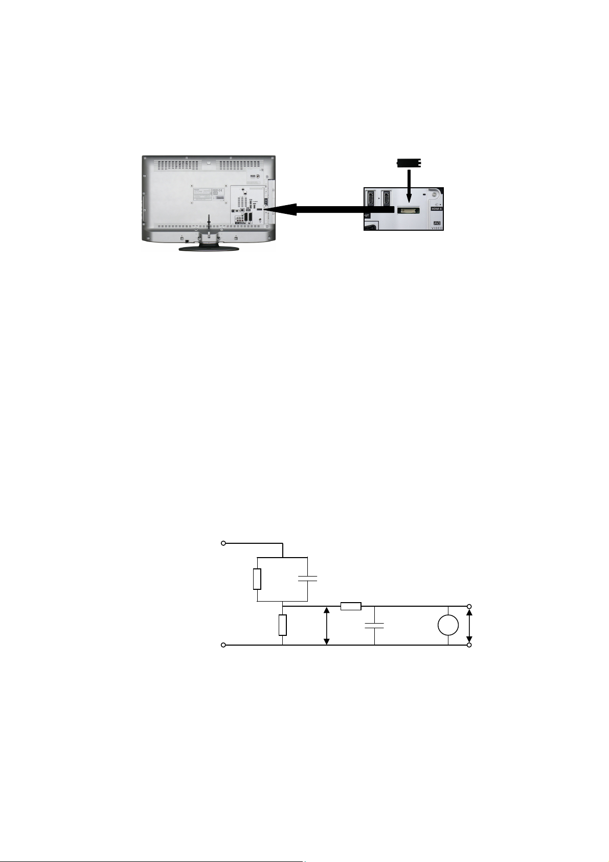
4. Always ensure panel TKP0E16001 is correctly replaced before returning to customer (see Fig.1).
Touch-Current Check
1. Plug the AC cord directly into the AC outlet. Do not use an isolation transfor mer for this check.
2. Connect a measuring network for touch currents between each exposed metallic part on the set and a good earth
ground such as a water pipe, as shown in Fig. 2.
3. Use Leakage Current Tester (Simpson 228 or equivalent) to measure the potential across the measuring network.
4. Check each exposed metallic part, and me asure the voltage at each point.
5. Reserve the AC plug in the AC outlet and re peat each of the above measure.
6. The potential at any point (TOUCH CURRENT) expressed as voltage U1 and U2, does not exceed the following values:
For a. c.: U1 = 35 V (peak) and U2 = 0.35 V (peak);
For d. c.: U1 = 1.0 V,
Note:
The limit value of U2 = 0.35 V (peak) for a. c. and U1 = 1.0 V for d. c. correspond to the values 0.7 mA (peak) a. c. and
2.0 mA d. c.
The limit value U1 = 35 V (peak) for a. c. correspond to the value 70 mA (peak) a. c. for frequencies greater than 100
kHz.
7. In case a measurement is out of the limits specified, there is a possibility of a shock hazard, and the equipment should
be repaired and rechecked before it is returned to the customer.
COLD
WATER PIPE
(EARTH GROUND)
TO
APPLIANCES
EXPOSED
METAL PARTS
Resistance values in ohms (Ω)
V: Voltmetr or oscilloscope
(r.m.s. or peak reading)
NOTE – Appropriate measures should be taken to obtain the correct value in case of non-sinusoidal waveforms
Measuring network for TOUCH CURRENTS
=1500Ω
R
S
Input resistance: ≥ 1M
Input capacitance: ≤ 200pF
Frequency range: 15Hz to 1MHz and d.c.respectively
R0=500Ω
Fig. 2
Fig. 1
C
=0.22μF
S
10k
F
0.022
V
U2 (V)
4

Prevention of Electrostatic Discharge (ESD) to Electrostatically
Sensitive (ES) Devices
Some semiconductor (solid state) devices can be damaged easily by static electricity. Such components commonly are
called Electrostatically Sensitive (ES) Devices. Examples of typical ES devices are integrated circuits and some field-effect
transistors and semiconductor "chip" components. The following techniques should be used to help reduce the incidence of
component damage caused by electrostatic discharge (ESD).
1. Immediately before handli ng any semiconductor component or semiconductor-equipped assembly, drain off any ESD on
your body by touching a known earth ground. Alternatively, obtain and wear a commercially available discharging ESD
wrist strap, which should be removed for potential shock reasons prior to applying power to the unit under test.
2. After removing an electrical assembly equipped with ES devices, place the assembly on a conductive surface such as
aluminum foil, to prevent electrostatic charge build up or exposure of the assembly.
3. Use only a grounded-tip s oldering iron to solder or unsolder ES devices.
4. Use only an anti-static solder removal device. Some solder removal devices not classified as "anti-static (ESD
protected)" can generate electrical charge sufficient to damage ES devices.
5. Do not use freon-propelle d chemicals. These can generate electrical charges sufficient to damage ES devices.
6. Do not remove a replacement ES device from its protective package until immediately before you are ready to install it.
(Most replacement ES devices are packaged with leads electrically shorted together by cond uctive foam, aluminum foil
or comparable conductive material).
7. Immediately before removing the protectiv e material from the le ads of a replacement ES device, touch the protective
material to the chassis or circuit assembly into which the device will be installed.
Caution
Be sure no power is applied to the chassis or circuit, and observe all other safety precautions.
8. Minimize bodily motions when handling unpackaged replacement ES devices. (Otherwise harmless motion such as the
brushing together of your clothes fabric or the lifting of your foot from a carpeted floor can generate static electricity
(ESD) sufficient to damage an ES device).
There are special components used in this equipment which are important for safety.
These parts are marked by in schematic diagrams, exploded views and replacement parts list. It is essential that
these critical parts should be replaced with manufacturer’s specified parts to prevent shock, fire, or other hazards. Do
not modify the original design without permission of manufacturer.
IMPORTANT SAFETY NOTICE
5
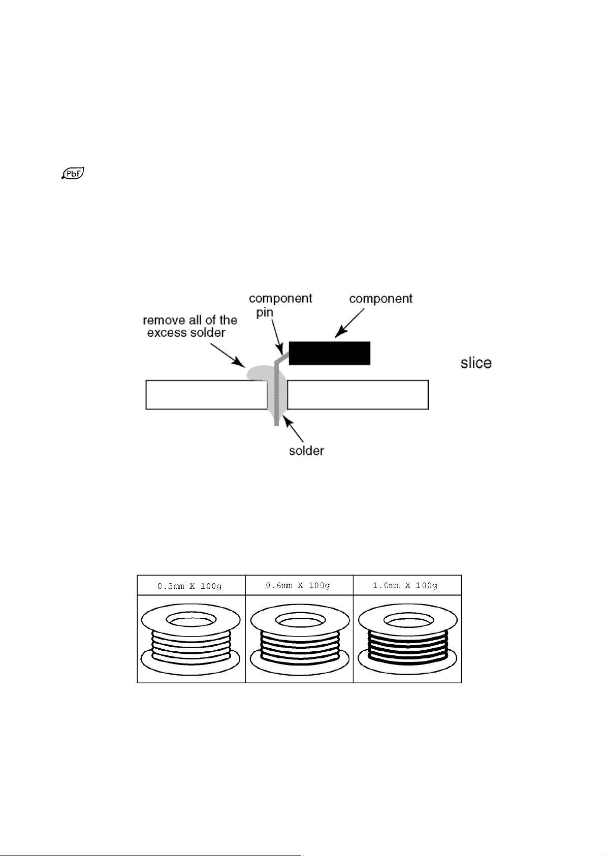
About lead free solder (PbF)
Note: Lead is listed as (Pb) in the periodic table of elements.
In the information below, Pb will refer to Lead solder, and PbF will refer to Lead Free Solder.
The Lead Free Solder used in our manufacturing process and discussed below is (Sn+Ag+Cu).
That is Tin (Sn), Silver (Ag) and Copper (Cu) although other types are available.
This model uses Pb Free solder in it’s manufacture due to environmental conservation issues. For service and repair work,
we’d suggest the use of Pb free solder as well, although Pb solder may be used.
PCBs manufactured using lead free solder will have the PbF within a leaf Symbol
stamped on the back of PCB.
Caution
• Pb free solder has a higher melting point than standard solder. Typically the melting point is 50 ~ 70 °F (30~40°C)
higher. Please use a high temperature soldering iron and set it to 700 ± 20 °F (370 ± 10 °C).
• Pb free solder will tend to splash when heated too high (a bout 1100 °F or 600 °C).
If you must use Pb solder, please completely remove all of the Pb free solder on the pins or solder area before
applying Pb solder. If this is not practical, be sure to heat the Pb free solder until it melts, before applying Pb solder.
• After applying PbF solder to double layered boards, please check the component side for excess solder which may
flow onto the opposite side. (see Fig.3)
Suggested Pb free solder
There are several kinds of Pb free solder available for purchase. This product uses Sn+Ag+Cu (tin, silver, copper) solder.
However, Sn+Cu (tin, copper), Sn+Zn+Bi (tin, zinc, bismuth) solder can also be used. (see Fig.4)
Fig.3
Fig.4
6
Applicable Signals
Component (Y, Pb, Pr), HDMI
525 (480) / 60i * *
525 (480) / 60p * *
625 (576) / 50i * *
625 (576) / 50p * *
750 (720) / 60p * *
750 (720) / 50p * *
1,125 (1,080) / 60i * *
1,125 (1,080) / 50i * *
1,125 (1,080) / 60p *
1,125 (1,080) / 50p *
1,125 (1,080) / 24p *
Applicable input signal for PC is basically compatible to VESA standard timing.
Signal name COMPONENT HDMI
PC (from D-sub 15P)
Signal name Horizontal frequency (kHz) Vertical frequency (Hz)
640 × 400 @70 Hz
640 × 480 @60 Hz
640 × 480 @75 Hz
800 × 600 @60 Hz
800 × 600 @75 Hz
800 × 600 @85 Hz
852 × 480 @60Hz
1,024 × 768 @60Hz
1,024 × 768 @70Hz
1,024 × 768 @75Hz
1,024 × 768 @85Hz
1,280 × 768 @60Hz
1,280 × 1,024 @60Hz
1,366 × 768 @60Hz
Macintosh 13“ (640 × 480)
Macintosh 16“ (832 × 624)
Macintosh 21“ (1,152 × 870)
PC (from HDMI terminal)
Applicable input signal for PC is basically compatible to HDMI standard timing.
Signal name Horizontal frequency (kHz) Vertical frequency (Hz)
640 × 480 @60 Hz
750 (720) / 60p 45.00 60.00
1,125 (1,080) / 60p 67.50 60.00
Note:
• Signals other than above may not be displayed properly.
• The above signals are reformatted for optimal viewing on your display.
• PC signal is magnified or compressed for displa y, so that it may not be possible to show fine detail
with sufficient clarity.
31.47 70.07
31.47 59.94
37.50 75.00
37.88 60.32
46.88 75.00
53.67 85.06
31.44 59.89
48.36 60.00
56.48 70.07
60.02 75.03
68.68 85.00
47.70 60.00
63.98 60.02
48.39 60.04
35.00 66.67
49.73 74.55
68.68 75.06
31.47 60.00
7
Service Hints
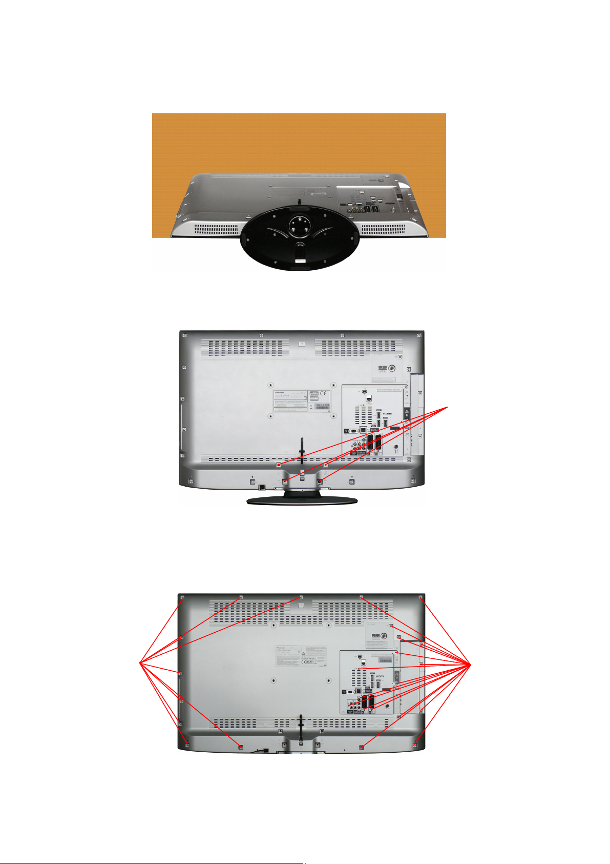
How to remove the back cover
Lay the main unit face down. (see Fig.5)
Remove the 4fixing screws and the pedestal assembly. (see Fig.6)
Remove the 26[24] fixing screws and the back cover. (see Fig.7)
SCREWS
Fig.6
Fig.7
SCREWS
SCREWS
8
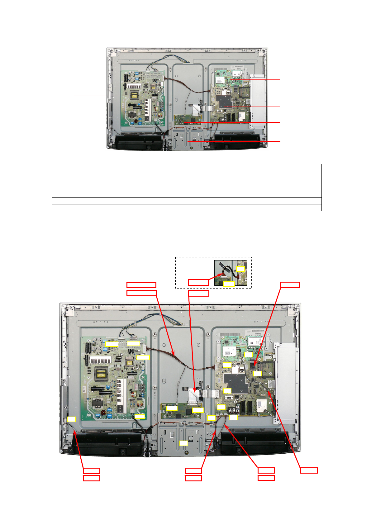
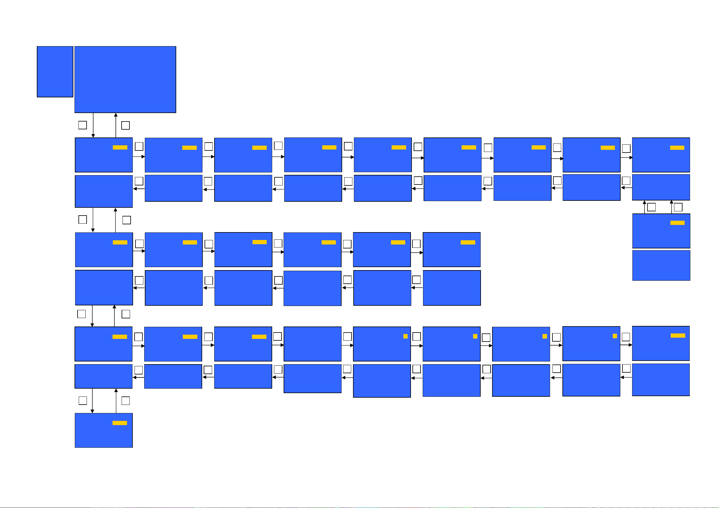
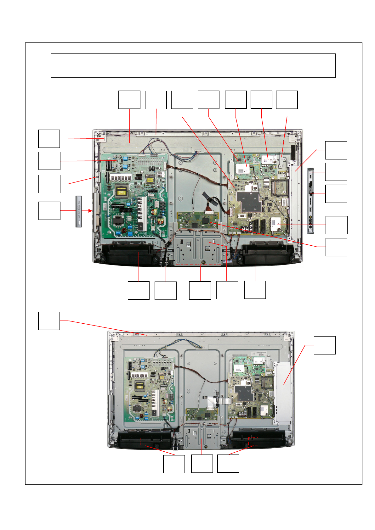
Chassis Board Layout
P-UNIT
Board Name Function
A-BOARD
V-BOARD Remote Receiver, R&G LED, Timer Rec LED, C.A.T.S.
P-UNIT Power Supply,Main Input
XW-BOARD Tuner DVB-T2 + DVB+S
TC-BOARD Panel Driver
AV Terminal, HDMI, AV Switch, Sound Processor, TV tuner, PC, LAN, OPT Terminal,
GENX, EEPROM, ADV, Speaker out,USB slot
Location of Lead Wiring
To find the Part Number of required wire in Replacement Parts List click on the wire name in red box.
XW -BOARD
A-BOARD
TC-BOARD
V-BOARD
TC05
A15
A88-XW2
A15 – TC05
(32’’)
(37’’)
A09-CN03-TC06
A09-CN03-TC06
(32’’)
(37’’)
A15 – TC05
CN01
CN02
CN03
XW2
A09
A88
A15
A12
A02
A10
K01
CNAC
TC06
TC05
V10
A02-K01
A02-K01
(32’’)
(37’’)
(32’’)
(37’’)
A12-SP
A12-SP
A10-V10
A10-V10
(32’’)
(37’’)
ATU-XTU
9
Technical Description
Specification of KEY for CI Plus, DTCP-IP and One-to-One
General information:
1. EEPROM (IC8950) for spare parts has the seed of KEY for each.
2. The final KEY data will be generated by LDA2 IC (IC8000) when SELF CHECK was done and are stored in both LDA2 IC
(IC8000) and EEPROM (IC8950).
Three KEY are not generated for all models.
The necessary KEY are only generated and stored depend on the feature of models.
Replacement of ICs:
When LDA2 IC (IC8000) is replaced, EEPROM (IC8950) should be also replaced with new one the same time.
When EEPROM (IC8950) is replaced, LDA2 IC (IC8000) is not necessary to be replaced the same time.
After the replacement of IC, SELF CHECK should be done to generate the final KEY data.
How to SELF CHECK: While pressing [VOLUME ( - )] button on the main unit, press [MENU] button on the remote
control for more than 3 seconds.
TV will be forced to the factory shipment setting after this SELF CHECK.
Model and Keys:
Model No.
TX-L37D25B None YES YES
TX-L32D26B None YES YES
TX-L32D25B None YES YES
CI PLUS DTCP-IP
Keys
One-to_one
(for USB Rec.)
10

Setting Inspection
Voltage Confirmation
A board
Description Test point Voltage
5.8VS TP2750 5.8V +/- 2%
STB_SUB_5.8V TP2789 5.8V +/- 2%
GND TP2785 0V
BL_SOS TP2780 0V
P17V TP2782 18V +/- 2%
SUB_F12V_15V TP2783 12V +/- 2%
SUB3.3 V TP5503 3.21V - 3.45V
SUB 1.5 V TP 5502 1.47V - 1.56V
SUB1.2V_A TP5500 1.26V - 1.33V
SUB1.2_D TP5501 1.26V - 1.33V
SUB5V TP5200 4.86V - 5.14V
SUB_OP_5V TP5300 4.92V - 5.31V
XW board
Description Test point Voltage
STB5.6V TP6700 5.51 - 6.09V
-SUB3.3V TP6701 3.135 - 3.465V
DTV15V TP6702 11.4 - 12.6 V
VDD1.0V TP6703 0.95 - 1.15V
IF3.3V TP6704 3.15 - 3.45 V
1.2V TP6851 1.08 - 1.32 V
5.0V TP6852 4.75 - 5.25 V
2.5V TP6937 2.30 - 2.70 V
TC board
Description Test point Voltage
ZW1.2V TP9061 1.17 - 1.31V
ZW3.3V TP9062 3.1 - 3.5V
LVCORE1.2V TP9205 1.10 - 1.25V
LVCC3.3V TP9208 3.1 - 3.5V
37” 32”
LVDD16V TP9210 14.5 - 15.5V 15.5 - 16.5V
VGH(25oC) TP9211 24.5 - 26.5V 26.0 - 28.0V
VGL TP9207 -7.8 - -7.2V -5.37 - -4.63V
H_VDD8V TP9206 6.85 - 7.35V 7.7 - 8.3V
11
Self Check
Self-check is used to automatically check the bus lines and hexadecimal code of the TV set. To enter Self-Check mode, keep
pressing the down (-/v) button on the TV set and press the STATUS button on the remote control. To exit Self Check,
switch off the TV set at the power button.
TX- L37D25B
TX- L32D26B
TX- L32D25B
If the CCU ports have been checked and found to be incorrect or not located then " - - " will appear in place of "O.K.".
37FHD Panasonic 2010LCD
Self Check Complete
TUN O.K.
STBY O.K.
MEM1 O.K.
MEM2 O.K..
ADAM O.K.
AVSW O.K.
OFDM O.K.
VIF O.K.
LAN O.K.
ZWEI O.K.
2nd FE O.K.
3rd FE O.K.
ID O.K.
32FHD Panasonic 2010LCD
Self Check Complete
TUN O.K.
STBY O.K.
MEM1 O.K.
MEM2 O.K..
ADAM O.K.
AVSW O.K.
OFDM O.K.
VIF O.K.
LAN O.K.
ZWEI O.K.
2nd FE O.K.
3rd FE O.K.
ID O.K.
PEAKS-SOFT 2.006
PEAKS-EEP 01.03.0013
LSI-PACKAGE 0.027
LSI-RELEASE 1.00
STBY-SOFT 1.00.00
STBY-EEP 1.08.3600
STBY-ROMCORR 1.01.00
ZWEI-SOFT 05000102
PEAKS-SOFT 2.006
PEAKS-EEP 01.03.0012
LSI-PACKAGE 0.027
LSI-RELEASE 1.00
STBY-SOFT 1.00.00
STBY-EEP 1.08.3600
STBY-ROMCORR 1.01.00
ZWEI-SOFT 05000102
SUM DABD
MODEL ID 07
03197100
00000010
EDID 53 0afaeda
SUM DB71
MODEL ID 07
03197100
00000004
EDID 53 0afaeda
32FHD Panasonic 2010LCD
Self Check Complete
TUN O.K.
STBY O.K.
MEM1 O.K.
MEM2 O.K..
ADAM O.K.
AVSW O.K.
OFDM O.K.
VIF O.K.
LAN O.K.
ZWEI O.K.
2nd FE O.K.
3rd FE O.K.
ID O.K.
PEAKS-SOFT 2.006
PEAKS-EEP 01.03.0012
LSI-PACKAGE 0.027
LSI-RELEASE 1.00
STBY-SOFT 1.00.00
STBY-EEP 1.08.3600
STBY-ROMCORR 1.01.00
ZWEI-SOFT 05000102
SUM DB71
MODEL ID 07
03197100
00000004
EDID 53 0afaeda
Display Ref. No. Description P.C.B.
TUN TU2901 TUNER A-Board
STBY IC1100 GENX A-Board
MEM1 IC1101 EEPROM GENX A-Board
MEM2 IC8950 EEPROM LDA2 A-Board
ADAM IC8000 A CHIP LDA2 A-Board
AVSW IC3000 AUDIO VIDEO SWITCH A-Board
OFDM IC8300 DIGITAL DEMODULATOR A-Board
VIF TU2901 TUNER A-Board
LAN IC8703 ETHERNET IF A-Board
ZWEI IC9006 ZWEI TC-Board
2nd FE TU6700 TUNER DVB-S XW-Board
3rd FE TU6851 TUNER DVB-T2 XW-Board
ID IC8950 EEPROM(LDA2) A-Board
12
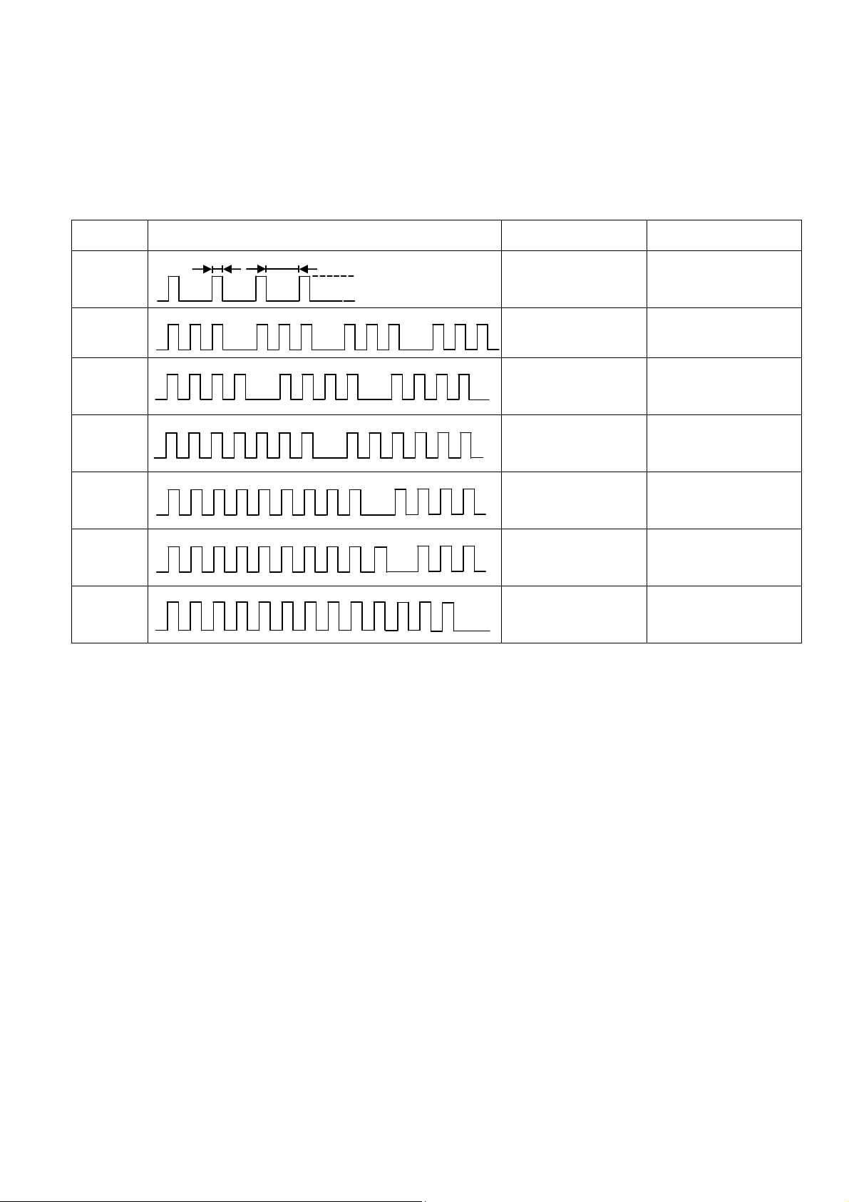
Power LED blinking timing chart
1. Subject
Information of LED Flashing timing chart.
2. Contents
When abnormality has occurred the unit, the protection circuit operates and reset to the stand by mode. At this time, the
defective block can be identified by number of blinking of the Power LED on the front panel of the unit.
Blinking
times
Once
1 BL_SOS
3
Blinking timing Contents Check point
4 sec
Light
No Light
SOS
A BOARD
P UNIT
A BOARD
XW BOARD
4
7
9
10
13
SUB_F_12V_SENSE
SOS
SUB_3.3V_SENSE
SOS
SOUND_SOS
ZWEI_SOS
Emergency SOS A BOARD
A BOARD
P UNIT
XW BOARD
A BOARD
XW BOARD
A BOARD
P UNIT
TC BOARD
13

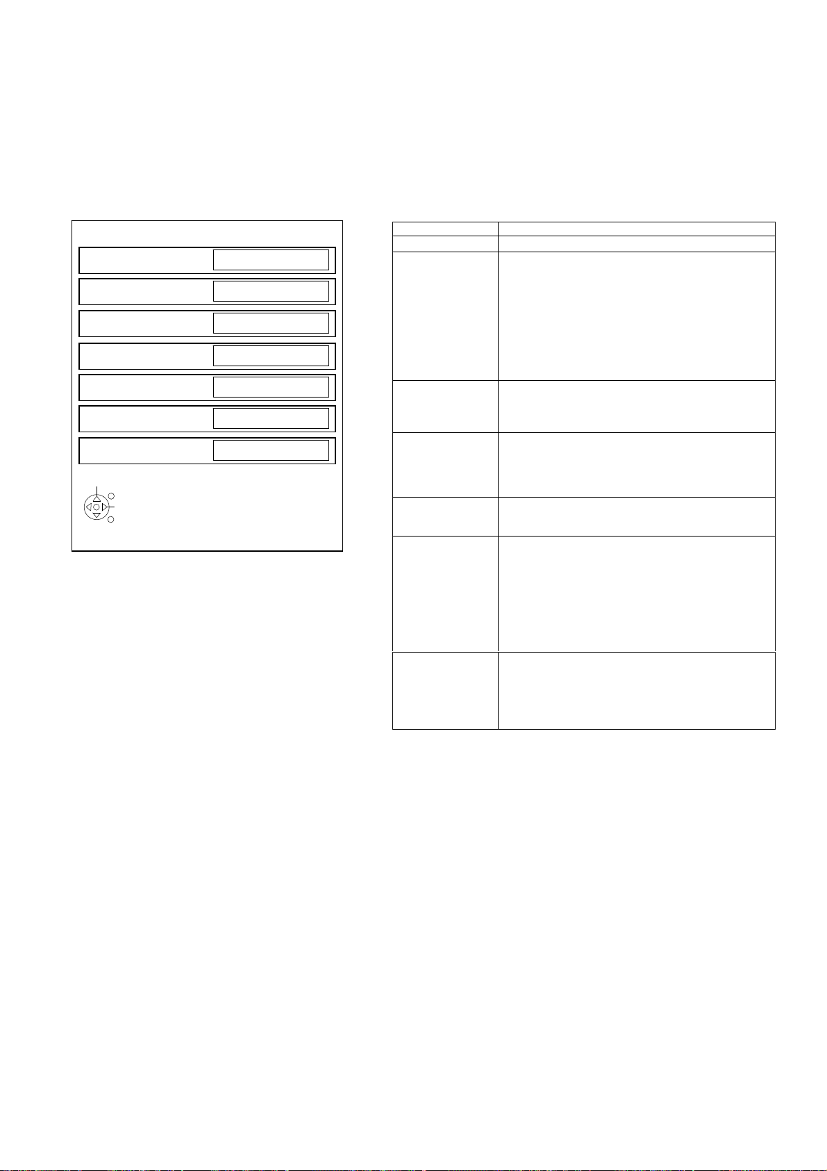
Service Mode Function
MPU controls the functions switching for each IICs through IIC bus in this chassis. The following setting and adjustment can
be adjusted by remote control in Service Menu
How to enter SERVICE
While pressing (-/v) button on the TV unit, press on the remote control for 3 times within 2 seconds.
Note:
To exit from Service mode, press the exit button on remote control.
0
14
SERVICE
A
A
A
A
A
A
SERVICE
ADJUST
WB-ADJ
OPTION
SRV-TOOL
Peaks SOFT 2.006 OPTION 1 3c
Peaks EEP 01.03.0012 OPTION 2 ef
LSI PACKAGE 1.00 OPTION 3 01
LSI RELEASE 0.00.16 OPTION 4 00
STBY SOFT 1.00.00 MODEL ID 07
STBY EEP 1.07.39 03197100
STBY ROMCOR 1.00.00 00000004
ZWEI SOFT 30000101 R/E Cnt 000/000
Ajax_CE 0.3.0 INV Cnt 0000
CMS data L0.403
1
ADJUST DYNAMIC
CONTRAST
YMAX
1,2:MAIN SELECT
3,4:SUB SELECT
9 :PICTURE MENU SELECT
YELLOW:AUTO ADJUST
VOL:ADJUST
OK :WRITE
1
WB-ADJ DYNAMIC
R-GAIN
BEFORE
METHOD
COLOR TEMP NORMAL
1,2:MAIN SELECT
3,4:SUB SELECT
7 :COLOR TEMP SELECT
9 :PICTURE MENU SELECT
0 :WB METHOD SELECT
VOL:ADJUST
OK :WRITE/WB DIFF ADJ
1
OPTION DYNAMIC
Boot
1,2:MAIN SELECT
3,4:SUB SELECT
9 :PICTURE MENU SELECT
VOL:ADJUST
1
SRV-TOOL DYNAMIC
000
FF
FF
02
ROM
00
2
ADJUST DYNAMIC
3
COLOR
1,2:MAIN SELECT
4
3,4:SUB SELECT
9 :PICTURE MENU SELECT
VOL:ADJUST
OK :WRITE
2
WB-ADJ DYNAMIC
G-GAIN
3
BEFORE
METHOD
COLOR TEMP NORMAL
1,2:MAIN SELECT
3,4:SUB SELECT
4
7 :COLOR TEMP SELECT
9 :PICTURE MENU SELECT
0 :WB METHOD SELECT
VOL:ADJUST
OK :WRITE/WB DIFF ADJ
2
OPTION DYNAMIC
STBY-SET
3
1,2:MAIN SELECT
4
3,4:SUB SELECT
9 :PICTURE MENU SELECT
OK :POWER OFF
2
31
E6
00
E6
02
DJUST DYNAMIC
3
TINT
1,2:MAIN SELECT
4
3,4:SUB SELECT
9 :PICTURE MENU SELECT
VOL:ADJUST
OK :WRITE
WB-ADJ DYNAMIC
B-GAIN
3
BEFORE
METHOD
COLOR TEMP NORMAL
1,2:MAIN SELECT
3,4:SUB SELECT
4
7 :COLOR TEMP SELECT
9 :PICTURE MENU SELECT
0 :WB METHOD SELECT
VOL:ADJUST
OK :WRITE/WB DIFF ADJ
OPTION DYNAMIC
Emergency
3
1,2:MAIN SELECT
4
3,4:SUB SELECT
9 :PICTURE MENU SELECT
VOL:ADJUST
Key Command
• Press the 3/4 button to change the adjustment values or function.
• Press the 1/2 button to step up/down through the functions and adjustments
• Press the numerical button VOLUME (+/-) to change option item.
• Press the OK button after each adjustment has been made to store the required values.
ON
00
CC
CC
02
ADJUST DYNAMIC
3
SUB-BRT
1,2:MAIN SELECT
4
3,4:SUB SELECT
9 :PICTURE MENU SELECT
VOL:ADJUST
OK :WRITE
WB-ADJ DYNAMIC
R-CENT
3
BEFORE
METHOD
COLOR TEMP NORMAL
1,2:MAIN SELECT
3,4:SUB SELECT
4
7 :COLOR TEMP SELECT
9 :PICTURE MENU SELECT
0 :WB METHOD SELECT
VOL:ADJUST
OK :WRITE/WB DIFF ADJ
OPTION DYNAMIC
Y/C Delay
3
1,2:MAIN SELECT
4
3,4:SUB SELECT
9 :PICTURE MENU SELECT
VOL:ADJUST
OK :WRITE
800
75
75
02
DJUST DYNAMIC
3
BACKLIGHT
1,2:MAIN SELECT
4
3,4:SUB SELECT
9 :PICTURE MENU SELECT
VOL:ADJUST
OK :WRITE
WB-ADJ DYNAMIC
G-CENT
3
BEFORE
METHOD
COLOR TEMP NORMAL
1,2:MAIN SELECT
3,4:SUB SELECT
7 :COLOR TEMP SELECT
9 :PICTURE MENU SELECT
0 :WB METHOD SELECT
VOL:ADJUST
OK :WRITE/WB DIFF ADJ
OPTION DYNAMIC
OPT 1
3
1,2:MAIN SELECT
4
3,4:SUB SELECT
5,6:BIT SELECT
9 :PICTURE MENU SELECT
VOL:ADJUST
OK :WRITE
554
80
80
02
00001100
DJUST DYNAMIC
H-POS
3
1,2:MAIN SELECT
4
3,4:SUB SELECT
9 :PICTURE MENU SELECT
VOL:ADJUST
OK :WRITE
WB-ADJ DYNAMIC
B-CENT
3
BEFORE
METHOD
COLOR TEMP NORMAL
1,2:MAIN SELECT
3,4:SUB SELECT
4 4
7 :COLOR TEMP SELECT
9 :PICTURE MENU SELECT
0 :WB METHOD SELECT
VOL:ADJUST
OK :WRITE/WB DIFF ADJ
OPTION DYNAMIC
OPT 2
3
1,2:MAIN SELECT
4
3,4:SUB SELECT
5,6:BIT SELECT
9 :PICTURE MENU SELECT
VOL:ADJUST
OK :WRITE
9F
02
11101110
9F
DJUST DYNAMIC
0
H-AMP
3
1,2:MAIN SELECT
4
3,4:SUB SELECT
9 :PICTURE MENU SELECT
VOL:ADJUST
OK :WRITE
OPTION DYNAMIC
OPT 3
3
1,2:MAIN SELECT
4
3,4:SUB SELECT
5,6:BIT SELECT
9 :PICTURE MENU SELECT
VOL:ADJUST
OK :WRITE
0
00000001
ADJUST DYNAMIC
V-POS
3
1,2:MAIN SELECT
4
3,4:SUB SELECT
9 :PICTURE MENU SELECT
VOL:ADJUST
OK :WRITE
OPTION DYNAMIC
OPT 4
3
1,2:MAIN SELECT
4
3,4:SUB SELECT
5,6:BIT SELECT
9 :PICTURE MENU SELECT
VOL:ADJUST
OK :WRITE
00000000
DJUST DYNAMIC
0
V-AMP
3
1,2:MAIN SELECT
4
3,4:SUB SELECT
9 :PICTURE MENU SELECT
VOL:ADJUST
OK :WRITE
4
DJUST DYNAMIC
VCOM
BEFORE
1,2:MAIN SELECT
3,4:SUB SELECT
5 :FLICKER PATTERN
9 :PICTURE MENU SELECT
VOL:ADJUST
OK :WRITE
OPTION DYNAMIC
EDID-CLK
3
HDMI
1,2:MAIN SELECT
4
3,4:SUB SELECT
7 :HDMI SELECT
9 :PICTURE MENU SELECT
VOL:ADJUST
OK :WRITE
3
17C
17C
MID
1
0
15

Service Tool Mode
How to access
1. Select [SRV-TOOL] in Service Mode.
2. Press [OK] button on the remote control.
Display of TD2Microcode version
Display of Flash ROM maker code
Display of SOS History
SRV-TOOL
TD2Microcode:005a0910
Flash ROOM: AD – F1
PTCT:00.00.00.00.00 Time 00051:30 On/Off 0000042
Display of SOS History
SOS History (Number of LED blinking) indication.
From left side; Last SOS, before Last, three occurrence before, 2
This indication will be cleared by [Self/check indication and forced to factory shipment setting].
nd
occurrence after shipment, 1st occurrence after shipment.
Power ON Time, On/Off
Note: To display TIME/COUNT menu, highlight position, then press MUTE for 3sec.
Time: Cumulative power on time, indicated hour: minute by decimal.
On/Off: Number of On/Off switching by decimal.
Note: This indication will not be cleared by either of the self-checks or any other command.
Exit
Disconnect the AC cord from wall outlet or switch off the power with [Power] button on the main unit.
POWER ON TIME/COUNT
Press [MUTE] button (3sec)
16
Hotel Mode
1. Purpose
Restrict a function for hotels.
2. Access command to the Hotel mode setup menu.
In order to display the Hotel mode setup menu,
please enter the following command (within 2 second).
[TV] : Vol.[Down] + [REMOTE] : AV (3 times)
Then, the Hotel mode setup menu is displayed.
Hotel mode
Hotel mode
Initial INPUT
Initial POS
Off
Off
Off
Initial VOL Level
Maximum Vol Level
Button Lock
Remote Lock
Off
Off
Off
Off
Select
EXIT
Change
RETURN
3. To exit the “Hotel mode” menu press the EXIT
button on remote control.
4. Explain the Hotel mode setup menu.
ITEM Function
Hotel Mode Select hotel mode ON/OFF
Initial INPUT Select input signal modes.
Initial POS Select programme number.
Initial VOL Level Adjust the volume when each time power is
Maximum VOL
Level
Button Lock Select local key conditions.
Remote Lock Select remote control key conditions.
Set the input, when each time power is switched on.
Selection:
Off Analog /DVB-C/DVB-T/T2 DVB-S
AV1/AV2/AV2S/AV3/
Component/PC/HDMI1/HDMI2/HDMI3/HDMI4
*Off: give priority to the last memory. However, Euro
Model is compulsorily set to TV.
*AVnS/AVnC: only Euro model selectable
* PC:selectable with VGA option
Selection:
Off/0 to 99
*Off: give priority to the last memory
switched on.
Selection/Range:
Off/0 to 100
*Off: give priority to the last memory
Adjust maximum volume.
Range:
0 to 100
Selection:
Off/SETUP/MENU/ALL
*Off: altogether valid
*Setup: only F-key is invalid
(Tuning guide (menu) can not be selected.)
*MENU: only F-key is invalid
(only Volume/Mute can be selected.)
*All: altogether invalid.
Selection:
Off/SETUP/MENU
*Off: altogether valid
*Setup: only Setup menu is invalid
MENU: Picture/Sound/Setup menu are invalid
17
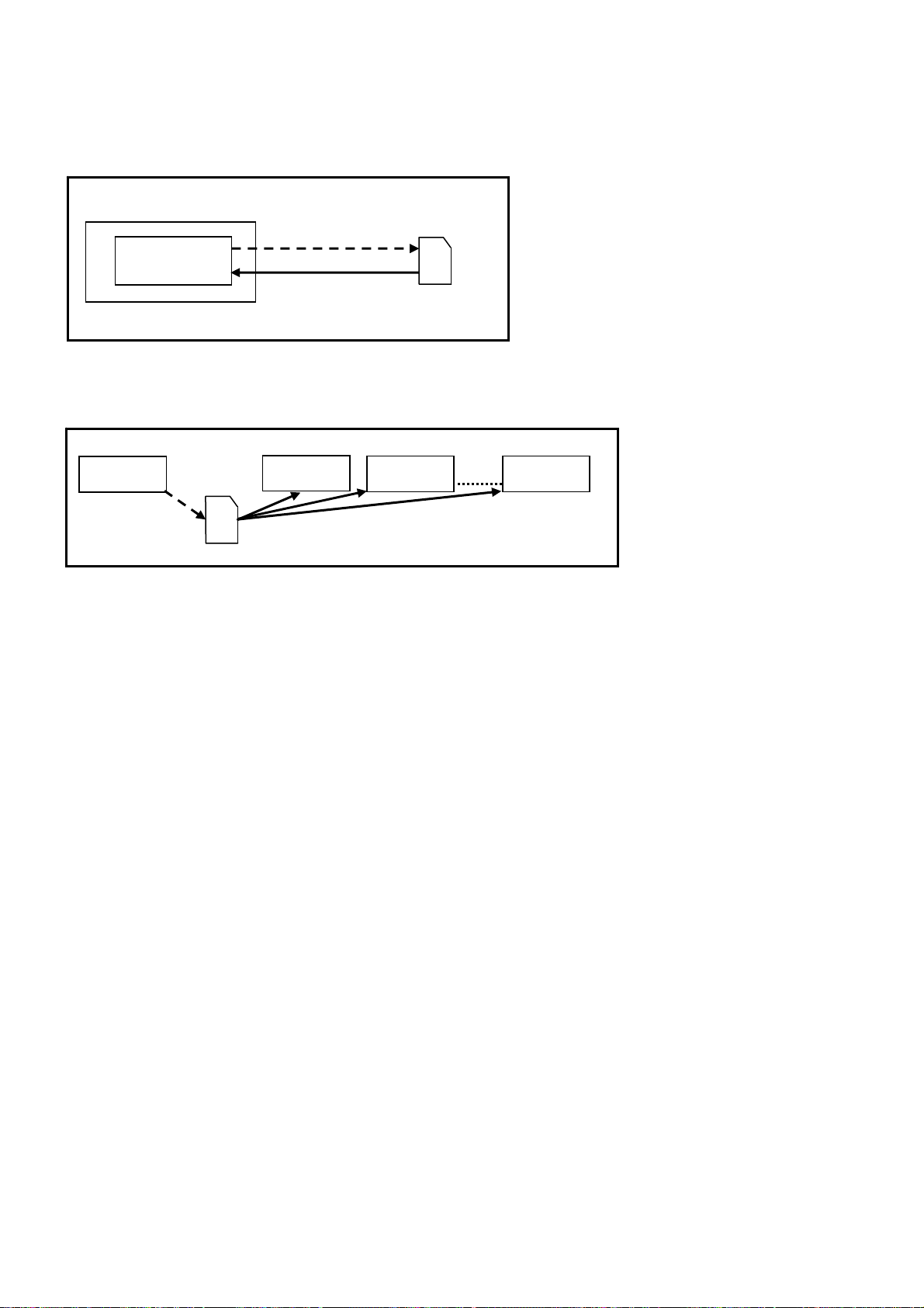
Data Copy by SD Card
Purpose
a) Board replacement (Copy the data when exchanging A-board):
When exchanging A-board, the data in original A-board can be copied to SD card and then copy to new A-board.
TV
A-board
(Before exchanging)
Copy to SD card
(After exchanging)
Copy back from SD card
SD
Following data can be copied.
User setting data
(inc. Hotel mode setting data)
Channel scan data
Adjustment and factory preset data
b) Hotel (Copy the data when installing a number of units in hotel or any facility):
When installing a number of units in hotel or any facility, the data in master TV can be copied to SD card and the copy
to other TVs.
Master TV
Copy to SD card
SD
Other TV
Copy from SD card
Other TV
Other TV
Following data can be copied.
User setting data
(inc. Hotel mode setting data)
Channel scan data
Preparation
Make pwd file as startup file for (a) or (b) in an empty SD card.
1. Insert an empty SD card to your PC.
2. Right-click a blank area in a SD card window, point to New and then click text document. A new file is created by
default (New Text Document.txt).
3. Right-click the ne w text docum ent that you just created and select rename and then change the name and extension of
the file to the following file name (a) or (b) and press ENTER.
File name:
(a) For Board replacement: boardreplace.pwd
(b) For Hotel: hotel.pwd
Note:
Please make only one file to prevent the operation error.
No any other file should be in SD card.
18
Data Copy from TV set to SD Card
1. Turn on the TV set.
2. Insert SD card with a startup file (pwd file) to SD slot.
On-screen Display will be appeared according to the startu p file automatically.
3. Input a following password for (a) or (b) by using remote control.
(a) For Board replacement: 2770
(b) For Hotel: 4850
Data will be copied from TV set to SD card.
It takes around 2 to 6 minutes maximum for copying.
4. After the completion of copying to SD card, remove SD card from TV set.
5. Turn off the TV set.
Note:
Following new folder will be created in SD card for data from TV set.
(a) For Board replacement: user_setup
(b) For Hotel: hotel
Please do not remove the SD card
Data copy has been successful
Data Copy(Board replacement )
Input password
Data Copy(Board replacement )
Input password
Data Copy(Board replacement )
Copy TV to SD card
Please wait for a while
Data Copy(Board replacement )
Performing
Please remove SD card
Data copy
(Board replacement) or (Hotel)
-----
Input Password
2770 or 4850
-----
Performing
GETTING
Completion
FINISH
19
Data Copy from SD Card to TV set
1. Turn on the TV set.
2. Insert SD card with Data to SD slot.
On-screen Display will be appeared according to the Data folder automaticall y.
3. Input a following password for (a) or (b) by using remote control.
(a) For Board replacement: 2771
(b) For Hotel: 4851
Data will be copied from SD card to TV set.
4. After the completion of copying from SD card, remove SD card from TV set.
(a) For Board replacement: Data will be deleted after copying (Limited one copy).
(b) For Hotel: Data will not be deleted and can be used for other TVs.
5. Turn off the TV set.
Note:
1. Depending on the failure of boards, function of Data for board replacement does not work.
2. This function can be effective amon g the same model numbers.
Data Copy(Board replacement )
Input Password
Input password
Performing
Data Copy(Board replacement )
Copy SD card to TV
Please wait for a while
Please do not remove the SD card
Data Copy(Board replacement )
Performing
Data copy has been successful
Please remove SD card
Input Password
2771 or 4851
-----
Performing
WRITING
Completion
FINISH
20

Option Bytes Description
OPTION1
b0 ATP Search Speed Slow (1) / Fast (0)
b1 TXT Ch Refresh On (1) / Off (0)
b2 ID-1 On (1) / Off (0)
b3 Macrovision Auto-Judge On (1) / Off (0)
b4 Surround enable low bit (*1) On (1) / Off (0)
b5 Surround enable low bit (*1) On (1) / Off (0)
b6 Pre Emphasis On (1) / Off (0)
b7 TINT_COMPONENT_HDMI On (1) / Off (0)
OPTION2
b0 Adjust lgain enable On (1) / Off (0)
b1 A2 BC enable (5.5) On (1) / Off (0)
b2 A2 DK1 enable (6.26) On (1) / Off (0)
b3 A2 DK3 enable (5.742) On (1) / Off (0)
b4 NICAM scan On (1) / Off (0)
b5 NICAM BG enable (5.5) On (1) / Off (0)
b6 NICAM I enable (6.0) On (1) / Off (0)
b7 NICAM DK enable (6.5) On (1) / Off (0)
OPTION3
b0 NICAM priority On (1) / Off (0)
b1 Starhub scan enable On (1) / Off (0)
b2 add H264 enable On (1) / Off (0)
b3 A2 DK2 enable On (1) / Off (0)
Inhibition of countermeasure for
b4
SIF signal drop
b5 get onid from physical CH On (1) / Off (0)
b6
b7 SASO mute On (1) / Off (0)
OPTION4
b0 All country DVB-S enable On (1) / Off (0)
b1 All country DVB-C enable On (1) / Off (0)
b2 3DYC color motion detected On (1) / Off (0)
b3 On (1) / Off (0)
b4 On (1) / Off (0)
b5 On (1) / Off (0)
b6 PIP On (1) / Off (0)
b7 RF remote control On (0) / Off (1)
On (1) / Off (0)
21

Adjustment Method
Sub-Contrast/White Balance Adjustment
Instrument Name Connect to Remarks
1. Remote controller
2. LCD WB meter (Minolta CA-210 or eq uivalent)
3. Comunication jig
4. Computer for external control
Procedure Remarks
Subcontrast adjustment
1. Receive PAL colour bar (10 0% white) RF signal.
2. Enter “Contrast” adj. In SERVICE mode.
3. Start adjusting by using Yellow Key.
4. If the adjustment finished normally, the letter of Contrast will change from red
to black.
White Balance adjustment
1. Procedure basically performs checking using the production software and
make automatic adjustment using external computer.
2. It adjusts in the mode of: Colour balance Normal
Viewing Mode Dynamic
Normal
Highlight x: 0.2710 ± 0.010
y: 0.2750 ± 0.010
Normal
Lowlight x: 0.2710 ± 0.010
y: 0.2750 ± 0.010
Correlation can be also taken by
CS-1000A or equivalent
Let the panel standfor more than 3
hours at more than 20 °C.
Basically perform adjustment in the
ambient environment of room
temperature more than 20 °C.
The aging time is more than20 min
at above room temperature.
Applied signal
100% full colour bar
0.7V p-p white peak
85% modulation
100% WHITE
50% GRAY
22
Wiring diagram
HDMI1
ETHERNET
JK8800
JK4700
HDMI2
JK4703
HDMI3
JK4701
HDMI4
JK4702
LCD PANEL
TC04
TC01
D3300
DIGITAL
AUDIO OUT
CN8850
SD SLOT
CN0100
SERVICE
USB0
JK8700A
USB1
JK8701
CN8940
CI SLOT
HP OUT
JK3300
V-IN,AUDIO IN,
A-BOARD
A15
A09
A10
TC05
TC06
CN03
V10
TC-BOARD
P UNIT
V-BOARD
CN01
CN02
MAIN IN
CNAC
JK3301
AUDIO OUT
YUV,AUDIO IN,
JK3304
PC
JK3302
AV1
JK3303
AV2
TU2901
TUNER
A02
KEY
A12
SP
23
A88
XW2
TU6700
DVB-S
TUNER
TU6851
TUNER
DVB-T2
XW-BOARD
Block Diagram (1/2)
A-BOARD
TNR5V
2
FE 1.2V
10
SUB3.3V
15
IFD1/2 19,20
TU2901
SIF-OUT 9
TUNER DVB-T/C
VIDEO OUT 11
IFD1/2
SIF
MAIN RF CVBS
CVBSin4
5
TO XW BOARD
1 2 3 5 7 15 16 17 19 20 22 23 24 26
A88
SUB3.3V
SUB_F12V/15V
IC3000
(C1AB00003218)
AVSW
STB5.8V
IFD1/2
2.5V
IC8302
(C0DBFYY00041)
FE TS PARALLEL
IC8300
(C1AB00003188)
OFDM
37,38
30,42,7
32,40
19
SUB3.3V
28,32,44
22,10
FE 1.2V
IC8360/1/2
TS-SW
16
SUB3.3V
CN8940
CI SLOT
SUB CI 5V
IC8400
(C1AB00003193)
CI TS ASIC
64,15
24,37
SUB3.3V
49
SUB5V
IC8401
(C1AB00002913)
LEVEL SHIFER ASIC
2,17,33
49
HS DATA
SUB3.3V
SUB5V
JK8701
IC8701
(C0DBZYY00266)
POWER SUPPLY
2,3
SUB 0P 5V
USB1
(C0DBZYY00266)
POWER SUPPLY
USB DATA
IC8700
2,3
SUB 0P 5V
JK8700A
USB0
USB DATA
AV1_V 20
AV1_VOUT 19
AV1_RED 15
AV1_GREEN 11
AV1_BLUE 7
JK3302
JK3303
AV1_L 6
AV1_LOUT 3
AV1_R 2
AV1 21PIN SCART
AV1_ROUT 1
AV2_V 20
AV2_VOUT 19
AV2_RED/C 15
AV2_GREEN 11
AV2_BLUE 7
AV2_L 6
AV2_LOUT 3
AV2 21PIN SCART
AV2_R 2
AV2_ROUT 1
1
2
PC
3
JK3304
Y
PB
PR
Y,PB,PR
L
L
IN
JK3301
R
L
AUDIO
R
OUT
SIDE AV
JK3300
TERMINAL
A09
3
3
7
7
9
9-10
10
12
12
13
13
TO P-UNIT
SUB ON
5
MAIN ON
4
ALARM
2
ON/OFF
1
STB 5.8V
P17V
SUBF12 15V
DCDCIN
STB SUB 5.8V
5.8VS
YPBPR-Y
YPBPR-PB
YPBPR-PR
AUDIO L IN
AV3_VIN
AV3_LIN
AV3_RIN
HP_LOUT
HP_ROUT
PC-R
PC-G
PC-B
SUB F12V 15V
DCDCIN
DCDCIN
P17V
79 CVBSIN6
44 CVBS/Y +COUT3
91 PRIN2/R3
89 CYIN2/G3
87 PBIN2/B3
62 L3IN
56 L1OUT
63 R3_IN
55 R1_OUT
23 CVBS_IN2
19 G1/YIN1
38 Y/Y+C/CVBSOUT4
37 SAG CVBSOUT4
11 R2/CIN3
21 B1 CIN1
13 G2/YIN2
15
64 L4IN
54 L2OUT
65 R4IN
53 R2OUT
3
2 GIN
1 BIN
95 CYIN1
93 PBIN1
97 PRIN1
70 L7IN
71 R7IN
52 L3OUT
51 R3OUT
81
68 L6IN
69 R6IN
IC5500
(C0DBAYY00715)
20
IC5501
(C0DBAYY00715)
20
R5266
R5265
B2/CIN2
RIN
CVBS IN5
4
9
4
9
Q5241
SUB1.2V_A
SUB1.2V_D
SUB1.5V
SUB3.3V
MAIN SND 17V
PNL 12V
G/CY/CVBSout1 31
B/PB/Cout1 33
R/PRout1 35
CVBSout 46
VDout 34
HDout 32
CVBSin1 17
R4out 49
L4out 50
L1IN 58
R1IN 59
L2IN 60
R2IN 61
SUB F12V 15V
STB 5.8V
MAIN Y/CVBS
MAIN PB/C
MAIN PR
RGB CVBS
PC VS
PC HS
DVB CVBS
AV - R
AV - L
AUDIOOUT L
AUDIOOUT R
TV OUT L
TV OUT R
SUB OP 5V
SUB 5V
STB SUB 5.8V
STB SUB 5.8V
TNR 5V
IC5280
(C0DBGYY00281)
4 3
SIF
2
3
(C0DBAYY00755)
1
8
(C0DBEYY00124)
4
(C0DBGYY00281)
5
STB 5V
SIF INN
SIF INP
HP_LOUT
HP_ROUT
IC5300
REG
IC5200
REG
IC2952
REG
DDC1
JK4701
CEC
HDMI3
SUB 3.3V
SUB 1.2V D
VDDSD
POWER SUPPLY
A-CHIP
B9
A9
A4
A5
A6
A7
P1
P2
E18
AV / IO
C15
A15
B13
A13
D13
C13
B14
A14
HDMI
HPD1
HDMI_5V_DET1
SUB 1.5V D
IC4700
HDMI SWITCH
(C1AB00003079)
3.3V HDMI
DDC2
CEC
HPD2
HDMI_5V_DET2
HDMI1
JK4700
IIC1 EEP
A-Chip
(HSDATA)
D-ChipA-Chip
OVP Circuit
P17V
SUBF12_15V
STB SUB8.8V
IC4701
(C0DBGYY00578)
REG
5
DDC1
CEC
HPD1
HDMI2
JK4703
SUB3.3V
8
IC8950
(C3EBJC000055)
EEPROM LDA2
IIC /IF
SUB OP 5V
4
SUB 5V
ARC
HDMI 5V DET1
OVP DET
IC5000
Analog
(AN34042A-VF)
STB5V
5.8VS
DDC0
HDMI4
JK4702
ASIC
STB3.3V
CEC
SUB3.3V
HPD0
IC8240,IC8241
DDR3 2x 1Gbit
DDR3 I/F
(MN2WS0110C)
STB XRST
PWM9V
SUB_F12V_15V
HDMI CEC
HDMI_5V_DET0
SUB3.3V
D3300
DIGITAL
AUDIO OUT
SUB3.3V
12,37
IC8000
LDA2
IC1100
GenX8
(MNZSFH9GP91)
HDMI 5V DET0,1,2,3
HPD0,1,2,3
DDC0,1,2,3
OPT SPDIF
IC8921
(C3FBTY000011)
NAND FLASH
EXTERNAL BUS
SERIAL
COMMUNICATION
IIC1
ADJ SCL/SDA
SG GENX KEY1
SWITCH
ARC
CPU BUSTS IF
D20 OPT AUDIO OUT
SERIAL I/F SDA/SCL
ETHER PHY
24,39,62
88,68,64
STB 3.3V
STB-5.8V
1 2 3
A02
TO K BOARD
HS DATA
DATA
IIC1
5.8VS
AUDIO OUT
EEP WP
IIC1 EEP
KEYSCAN
USB I/F
SDA/SCL
LVDS I/F
POWER SUPPLY
D-CHIP
(C3EBFC000047)
STB 3.3V
SUB3.3V
SD CARD
CN8850
F20
E19
C19
B19
IC1101
EEPROM
8
FOR ADJUSTMENT
IIC2
SUB 3.3V
SUB 1.2V D
SUB 1.5V D
VDDSD
DDR1.5V
MAIN SND 17V
STB 5V
GenX8 E2PROM
SERVICE
CN0100
SDA/SCL
IC2952
(C0DBGYY00281)
REG
IC2950
(C0CBCAG00031)
REG
LVDS RGB 10bit
8
IC2301
9
AUDIO AMP
(C1AB00003230)
14
15
MAIN SND 17V
IC5220
(C0DBGYY00895)
REG
(C1CB00003239)
25,26
STB SUB5.8V
4
TNR 5V
1
SUB3.3V
6
FE1.2V
1
25-26
30-31
36-37
41-42
SUB F12V 15V
3
SUB 9V
1
IC8703
ETHERNET
9-12
SUB3.3V
RX/TX
SUB3.3V
ETHERNET
LAN
JK8800
PNL 12V
REMOTE
AI SENSOR
G LED
R LED
SUB5V
STB3.3V
A15
1-5
42-44
46-47
37-40
32-36
30-27
24-21
20-16
14-11
A12
4
3
2
1
A10
6
5
3
2
8
4
TO T-CON BOARD
SP- R
SP- L
TO V-BOARD
24
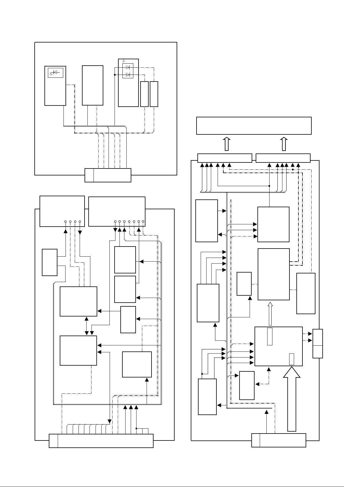
Block Diagram (2/2)
AI
SN2500
(B3JB0000078)
3 1
RM2500
VCC OUT
(PNJ4815M01TV)
STBY 3.3V
VCC
3
SUB 5V
OUT
1
AI
STBY 3.3V
G
R
D2500
(B3AGB000060)
Q2500
R LED
Q2501
G LED
LCD PANEL
V-BOARD
TUNER
TU6851
DVB/T2
(ENV57S03D8F)
5
4
IC6856
(CODBAHF00015)
2,17 5V
STB 5.6V
IC6851
(C1AB00003273)
IC6852
14 SDA
19-20 IFD out
13 SCL
TUNER_CLK
58
DIGITAL
DEMODULATOR
IC6853
IC6854
(C0JBAR000566)
TUNER_DAT
57
TS I/F
SWITCH
V10
TUNER
49,50
1.2V
R LED
G LED
STBY 3.3V
1
23457
TO A10
TU6700
DVB/T-S/S2
(J3BBCBC00006)
SAT ST
1.2V
SUB 3.3V
AI
14-21 SAT MD
REMOTE
SUB 5V
11 SUB3.3V
13 VDD1.0V
IC6702
(C0DBAYY00462)
POWER SUPPLYV
IC6701
POWER SUPPLY
(C0DBEYY00123)
IC6855
4 3.3V
9 SCL
8 SDA
3.3V
(C0DBAYY00462)
IC6700
INTERFACE
REGULATOR
(C1AB00002948)
DISEQ IN/OUT
DTV 15V
STB 5.6V
DTV 15V
EXTM/DISEQ
RIGHT 60pin
VCC L3.3V
VDD L16V
H_VDD8V
H VDD8V
IC9205
(C0DBAYY00730)
STEP DOWN CONVERTER
PNL 12V
VCC L3.3V
VGH L20V
VGL -L10V
VDD 16V
IC9207
(C0DBAYY00731)
Gamma Voltage GEN.
PNL 12V
VDD 3.3V
ZW 1.2V
ZW 3.3V
DRIVER
VDD L16V
VCC L3.3V
SDA SCL
IC9202
SDA SCL
1.22V
3.3V
2.5V
3.3V
EEP
LVCC3.3V
SCL/SDA
DRIVER
LEFT 60pin
H_VDD8V
GMA 1-4
3-6
15-18
IC9206
(C0FBBY000076)
TCON GAMMA DAT
IC9201
(C1AB00003252)
TFL LCD PANEL CONTROLL
3-14
17-28
31-42
mini LVDS
IC9006
SPI
FLSH
VCC L3.3V
VDD L16V
92-95,97-100,102-105
107-108,110-111,113-116
118-121,123-124,126-127
CLK
ZWEI 2
(MN85061)
mini-LVDS
BL
LVDS
mini-LVDS
CLK 1-6
OUT 1-6
IN 1-6
IC9204
LEVEL SHIFTER
(C1AB00003246)
PWMB/PWMA
32
TC06
XW-BOARD
TS SYNC/VAL/CLK
XW1
1,3,5
789
TS SYNC/VAL/CLK
11
121415
XW1 TO A88
TS DATA
DTV 15V
IC9003
SPI ZWEI FLASH
IC9004
20
(C0DBAYY00715)
DC/DC CONVERTER
PNL 12V
LVDS RGB 10bit
SUB 3.3V
DTV 15V
SUB 3.3V
STB 5.6V
16
18
20
2426282930
TC-BOARD
9-10
TC05
PNL 12V
51-47
SDA SCL
5-6
37-40
32-36
30-27
24-21
20-16
14-11
TO A15
25
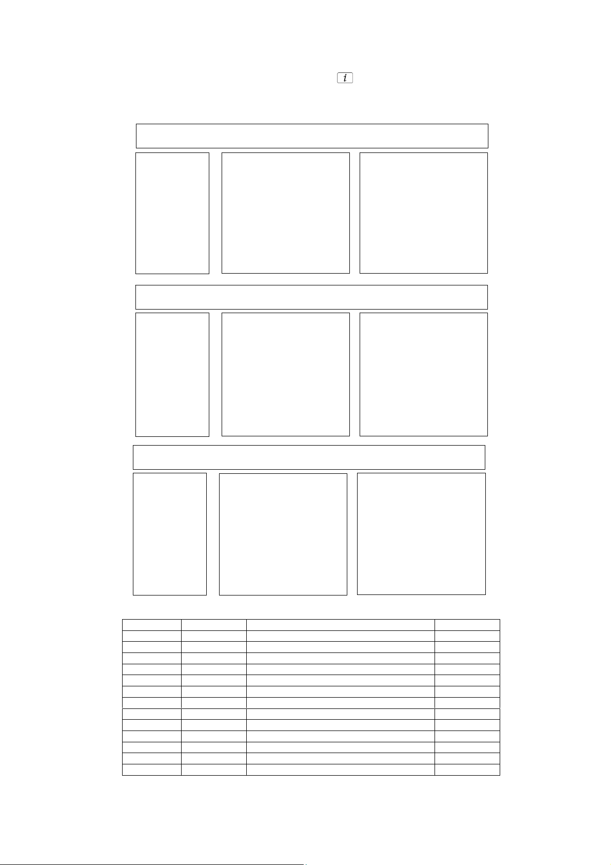
Parts Location
(UK)
The numbers on the exploded view below refer to the exploded view section of the Replacement Parts List.
6
17
NOTE:
16
23
18
8
28
24
26
Parts Location
The numbers on the exploded view below refer to the exploded view section of the Replacement Parts List.
19
22
NOTE:
15
13
2
3
11
10
5
9
4
22
27
12
14
20
Difference for 37’’
26
29
20
29
21
25
7
1
30
21
27
 Loading...