

Motorola MC145167P, MC145166P, MC145167DW, MC145166DW Datasheet
MC145166•MC145167MOTOROLA
1
CMOS
These devices are dual phase–locked loop (PLL) frequency synthesizers in–
tended for use primarily in 46/49 MHz cordless phones with up to 10 channels.
These parts contain two mask–programmable counter ROMs for receive and
transmit loops with two independent phase detect circuits. A common reference
oscillator and reference divider are shared by the receive and transmit circuits.
Frequency selection is accomplished via a 4–bit parallel input for the
MC145166. The MC145167 utilizes a serial interface.
Other features include a lock detect circuit for the transmit loop, illegal code
default, and a 5 kHz tone output.
• Synthesizes Up to Ten Channel Pairs
• Maximum Operating Frequency: 60 MHz @ V
in
= 200 mV p–p
• Operating Temperature Range: – 40 to + 75°C
• Operating Voltage Range: 2.5 to 5.5 V
• On–Chip Oscillator Circuit Supports External Crystal
• Lock Detect Signal
• Operating Power Consumption: 3.0 mA @ 3.0 V
• Standby Mode for Power Savings: 1.5 mA @ 3.0 V
• Also See MC145162
Order this document
by MC145166/D
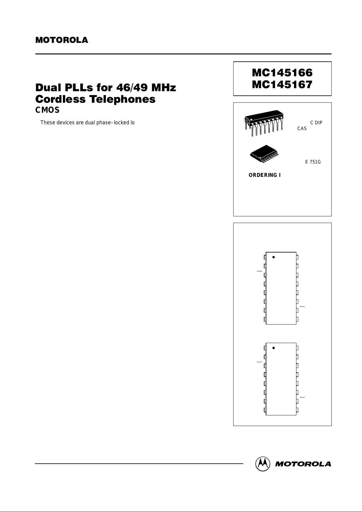
SEMICONDUCTOR TECHNICAL DATA
P SUFFIX
PLASTIC DIP
CASE 648
DW SUFFIX
SOG PACKAGE
CASE 751G
ORDERING INFORMATION
MC145166P Plastic DIP
MC145166DW SOG Package
MC145167P Plastic DIP
MC145167DW SOG Package
16
1
16
1
PIN ASSIGNMENTS
MC145166P
MC145166DW
13
14
15
16
9
10
11
125
4
3
2
1
8
7
6
V
SS
PD1
f
in1
V
DD
OSC
in
f
in2
LD
PD2
5 k
SB
MODE
OSC
out
D3
D2
D1
D0
MC145167P
MC145167DW
13
14
15
16
9
10
11
125
4
3
2
1
8
7
6
V
SS
PD1
f
in1
V
DD
OSC
in
f
in2
LD
PD2
5 k
SB
MODE
OSC
out
ENB
NC
CLK
DATA
NC = NO CONNECTION
Motorola, Inc. 1998
REV 2
1/98 TN98011400
MC145166•MC145167 MOTOROLA
2
BLOCK DIAGRAM
*On–chip pull–down.
OSC
out
OSC
in
f
in2
f
in1
DATA
CLK
ENB
4–BIT S/R
4–BIT LATCH
D3
D2
D1
D0
MODE
PD2
V
DD
PD1
f
v
=
5 kHz
DECODE
LOGIC
PHASE
DET 2
LOCK
DET
PHASE
DET 1
14
13
REFERENCE
COUNTER
DIVIDE–BY–2048
14–BIT
DIVIDE–BY–N
TRANSMIT
COUNTER
13–BIT DIVIDE–BY–N
RECEIVE COUNTER
SB
RECEIVE
ROM
TRANSMIT
ROM
*
5 kHz
f
v
LD
f
r
*
*
*
*
MC145166
ONLY
MC145167 ONLY
f
r
V
SS
5 k
MC145166•MC145167MOTOROLA
3
MAXIMUM RATINGS* (Voltages Referenced to V
SS
)
Symbol Rating Value Unit
V
DD
DC Supply Voltage – 0.5 to + 6.0 V
V
in
Input Voltage, All Inputs – 0.5 to VDD + 0.5 V
Iin, I
out
DC Current Drain Per Pin 10 mA
IDD, ISSDC Current Drain VDD or VSS Pins 30 mA
T
stg
Storage Temperature Range – 65 to + 150 °C
*Maximum Ratings are those values beyond which damage to the device may occur.
Functional operation should be restricted to the limits in the Electrical Characteristics
tables or Pin Descriptions section.
ELECTRICAL CHARACTERISTICS (Voltages Referenced to V
SS
, TA = 25°C)
Guaranteed Limit
Symbol Characteristic V
DD
Min Max
Unit
V
DD
Power Supply Voltage Range — 2.5 5.5 V
V
OL
Output Voltage 0 Level
(I
out
= 0)
2.5
5.5
—
—
0.05
0.05
V
V
OH
(Vin = VDD or 0) 1 Level 2.5
5.5
2.45
5.45
—
—
V
IL
Input Voltage 0 Level
(V
out
= 0.5 V or VDD – 0.5 V)
2.5
5.5
—
—
0.75
1.65
V
V
IH
1 Level 2.5
5.5
1.75
3.85
—
—
I
OH
Output Current (V
out
= 2.2 V) Source
(V
out
= 5.0 V)
2.5
5.5
– 0.18
– 0.55
—
—
mA
I
OL
(V
out
= 0.3 V) Sink
(V
out
= 0.5 V)
2.5
5.5
0.18
0.55
—
—
I
IL
Input Current OSCin, f
in1
, f
in2
(Vin = 0)
2.5
5.5
—
—
– 30
– 66
µA
DATA, SB, Mode 2.5
5.5
—
—
– 0.05
– 0.11
I
IH
(Vin = VDD – 0.5) OSCin, f
in1
, f
in2
2.5
5.5
—
—
30
66
µA
DATA, SB, Mode 2.5
5.5
—
—
50
121
C
in
Input Capacitance — — 14.0 pF
C
out
Output Capacitance — — 8.0 pF
I
DD
Standby Current, SB = VSS or Open 2.5
5.5
—
—
1.4
3.6
mA
I
dd
Operating Current
(200 mV p–p input at f
in1
and f
in2
, SB
= VDD)
2.5
5.5
—
—
2.8
6.2
mA
I
OZ
Three–State Leakage Current
(V
out
= 0 or 5.5 V)
5.5 — ± 1.0 µA
This device contains protection circuitry to
guard against damage due to high static voltages or electric fields. However, precautions
must be taken to avoid applications of any
voltage higher than maximum rated voltages
to this high–impedance circuit. For proper operation, Vin and V
out
should be constrained to
the range VSS≤ (Vin or V
out
) ≤ VDD.
Unused inputs must always be tied to an
appropriate logic voltage level (e.g., either V
SS
or VDD). Unused outputs must be left open.
MC145166•MC145167 MOTOROLA
4
SWITCHING CHARACTERISTICS (T
A
= 25°C, CL = 50 pF)
Figure
Guaranteed Limit
Symbol Characteristic
Figure
No.
V
DD
Min Max
Unit
t
TLH
Output Rise Time 1, 5 3.0
5.0
—
—
200
100
ns
t
THL
Output Fall Time 1, 5 3.0
5.0
—
—
200
100
ns
tr, t
f
Input Rise and Fall Time, OSC
in
2 3.0
5.0
—
—
5.0
4.0
µs
f
max
Input Frequency OSC
in
Input = Sine Wave 200 mV p–p f
in1
f
in2
3.0 – 5.0
3.0 – 5.0
3.0 – 5.0
—
—
—
12
60
60
MHz
t
su
Setup Time (MC145167) DATA to CLK 3 3.0
5.0
100
50
—
—
ns
ENB to CLK 3.0
5.0
200
100
—
—
t
h
Hold Time (MC145167), CLK to DATA 3 3.0
5.0
80
40
—
—
ns
t
rec
Recovery Time (MC145167), ENB to CLK 3 3.0
5.0
80
40
—
—
ns
t
w
Input Pulse Width (MC145167), CLK and ENB 4 3.0
5.0
80
60
—
—
ns
 Loading...