

Motorola MC10E131FN, MC10E131FNR2, MC100E131FN, MC100E131FNR2 Datasheet
5 6 7 8 9 10 11
Q
3
Q
3
V
CCO
R
2
CE
2
D
2
R
3
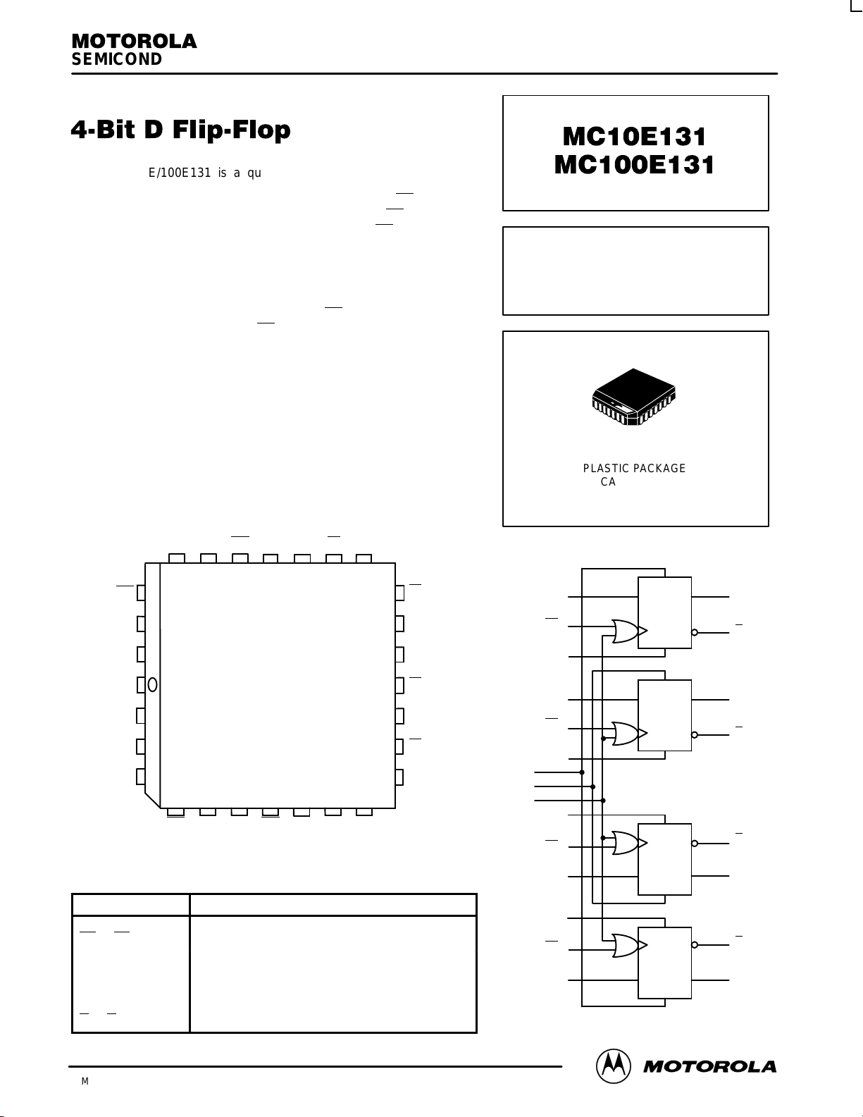
LOGIC DIAGRAM
CE
3
D
3
S
12
V
EE
C
C
S
03
D
0
26
27
28
2
3
4
25 24 23 22 21 20 19
18
17
16
15
14
13
12
Q
2
Q
2
V
CC
Q
1
Q
1
Q
0
Q
0
CE
0
R0D1CE1R1NC V
CCO
D
3
CE
3
R
3
D
2
CE
2
R
2
S
03
S
12
C
C
R
1
CE
1
D
1
R
0
CE
0
D
0
Q
3
Q
3
Q
2
Q
2
Q
1
Q
1
Q
0
Q
0
S
D
Q
Q
R
S
D
Q
Q
R
R
D
Q
Q
S
R
D
Q
Q
S
1
Pinout: 28-Lead PLCC (Top View)
* All VCC and V
CCO
pins are tied together on the die.
SEMICONDUCTOR TECHNICAL DATA
2–1
REV 3
Motorola, Inc. 1996
7/96
The MC10E/100E131 is a quad master-slave D-type flip-flop with
differential outputs. Each flip-flop may be clocked separately by holding
Common Clock (CC) LOW and using the Clock Enable (CE
) inputs for
clocking. Common clocking is achieved by holding the CE
inputs LOW
and using CC to clock all four flip-flops. In this case, the CE
inputs perform
the function of controlling the common clock, to each flip-flop.
Individual asynchronous resets are provided (R). Asynchronous set
controls (S) are ganged together in pairs, with the pairing chosen to
reflect physical chip symmetry.
Data enters the master when both CC and CE
are LOW, and transfers
to the slave when either CC or CE
(or both) go HIGH.
• 1100MHz Min. Toggle Frequency
• Differential Outputs
• Individual and Common Clocks
• Individual Resets (asynchronous)
• Paired Sets (asynchronous)
• Extended 100E V
EE
Range of – 4.2V to – 5.46V
• 75kΩ Input Pulldown Resistors
PIN NAMES
Pin Function
D0– D
3
Data Inputs
CE
0
– CE
3
Clock Enables (Individual)
R0– R
3
Resets
C
C
Common Clock
S03, S
12
Sets (paired)
Q0– Q
3
True Outputs
Q
0
– Q
3
Inverting Outputs
4-BIT
D FLIP-FLOP
FN SUFFIX
PLASTIC PACKAGE
CASE 776-02
MC10E131 MC100E131
MOTOROLA ECLinPS and ECLinPS Lite
DL140 — Rev 4
2–2
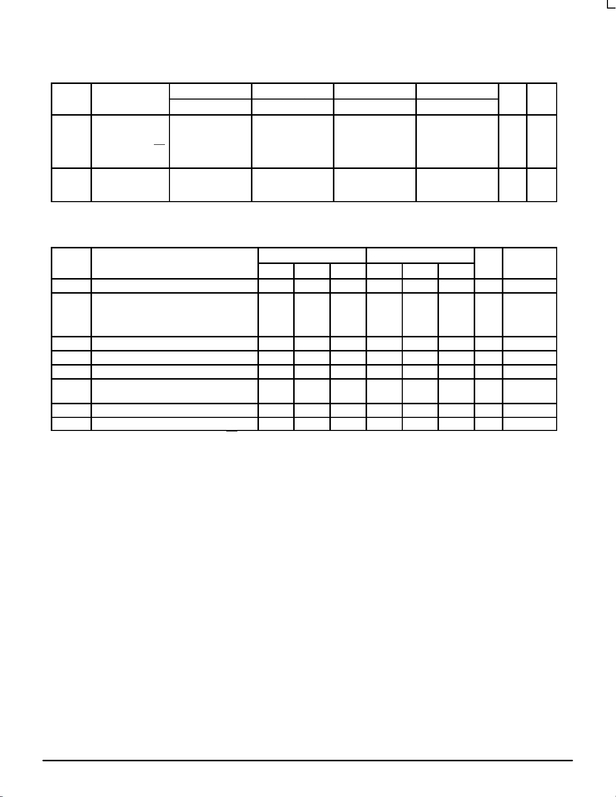
DC CHARACTERISTICS (VEE = VEE(min) to VEE(max); VCC = V
CCO
= GND)
–40°C 0°C 25°C 85°C
Symbol Characteristic Min Typ Max Min Typ Max Min Typ Max Min Typ Max Unit Cond
I
IH
Input HIGH
Current C
C
S
R, CE
D
350
450
300
150
350
450
300
150
350
450
300
150
350
450
300
150
µA
I
IEE
Power Supply
Current 10E
100E
585870
70
585870
70
585870
70
586770
81
mA
AC CHARACTERISTICS (VEE = VEE(min) to VEE(max); VCC = V
CCO
= GND)
–40°C 0°C to 85°C
Symbol Characteristic Min Typ Max Min Typ Max Unit Condition
f
MAX
Maximum Toggle Frequency 1000 1400 1100 1400 MHz
t
PLH
t
PHL
Propagation Delay to Output CE
C
C
R
S
310
275
300
300
600
600
625
550
750
725
775
775
360
325
350
350
500
500
550
550
700
675
725
725
ps
t
S
Setup Time D 200 20 150 20 ps 1
t
H
Hold Time D 225 –20 175 –20 ps 1
t
RR
Reset Recovery Time 450 150 400 150 ps
t
PW
Minimum Pulse Width CLK
R, S
400
400
400
400
ps
t
SKEW
Within-Device Skew 60 60 ps 2
tr/t
f
Rise/Fall Time 275 460 725 300 480 675 ps 20–80%
1. Setup/hold times guaranteed for both CC and CE.
2. Within-device skew is defined as identical transitions on similar paths through a device.
 Loading...