


 Loading...
Mitsubishi M32170F6VWG, M32170F6VFP, M32170F4VWG, M32170F4VFP, M32170F3VWG Datasheet
...
|
ADVANCED AND EVER ADVANCING |
|
|
|
|
|
|
|
|
Preliminary |
|
MSD-M32170-U-0003 |
||
|
|
|
|
|
Mitsubishi 32-bit RISC Single-chip Microcomputers
M32R Family M32R/E Series
32170
Group
M32170F6VFP/WG
M32170F4VFP/WG
M32170F3VFP/WG
User’s Manual
2000-03-17 Ver0.10
NOTE
Information in this manual may be changed without prior notice.
Mitsubishi Electric Corporation
Mitsubishi Electric Semiconductor Systems Corporation

Keep safety first in your circuit designs!
●Mitsubishi Electric Corporation puts the maximum effort into making semiconductor products better and more reliable, but there is always the possibility that trouble may occur with them. Trouble with semiconductors may lead to personal injury, fire or property damage. Remember to give due consideration to safety when making your circuit designs, with appropriate measures such as (i) placement of substitutive, auxiliary circuits, (ii) use of non-flammable material or (iii) prevention against any malfunction or mishap.
Notes regarding these materials
●These materials are intended as a reference to assist our customers in the selection of the Mitsubishi semiconductor product best suited to the customer's application; they do not convey any license under any intellectual property rights, or any other rights, belonging to Mitsubishi Electric Corporation or a third party.
●Mitsubishi Electric Corporation assumes no responsibility for any damage, or infringement of any third-party's rights, originating in the use of any product data, diagrams, charts, programs, algorithms, or circuit application examples contained in these materials.
●All information contained in these materials, including product data, diagrams, charts, programs and algorithms represents information on products at the time of publication of these materials, and are subject to change by Mitsubishi Electric Corporation without notice due to product improvements or other reasons. It is therefore recommended that customers contact Mitsubishi Electric Corporation or an authorized Mitsubishi Semiconductor product distributor for the latest product information before purchasing a product listed herein.
The information described here may contain technical inaccuracies or typographical errors. Mitsubishi Electric Corporation assumes no responsibility for any damage, liability, or other loss rising from these inaccuracies or errors.
Please also pay attention to information published by Mitsubishi Electric Corporation by various means, including the Mitsubishi Semiconductor home page (http:// www.mitsubishichips.com).
●When using any or all of the information contained in these materials, including product data, diagrams, charts, programs, and algorithms, please be sure to evaluate all information as a total system before making a final decision on the applicability of the information and products. Mitsubishi Electric Corporation assumes no responsibility for any damage, liability or other loss resulting from the information contained herein.
●Mitsubishi Electric Corporation semiconductors are not designed or manufactured for use in a device or system that is used under circumstances in which human life is potentially at stake. Please contact Mitsubishi Electric Corporation or an authorized Mitsubishi Semiconductor product distributor when considering the use of a product contained herein for any specific purposes, such as apparatus or systems for transportation, vehicular, medical, aerospace, nuclear, or undersea repeater use.
●The prior written approval of Mitsubishi Electric Corporation is necessary to reprint or reproduce in whole or in part these materials.
●If these products or technologies are subject to the Japanese export control restrictions, they must be exported under a license from the Japanese government and cannot be imported into a country other than the approved destination.
Any diversion or reexport contrary to the export control laws and regulations of Japan and/or the country of destination is prohibited.
●Please contact Mitsubishi Electric Corporation or an authorized Mitsubishi Semicon ductor product distributor for further details on these materials or the products con tained therein.
PREFACE
This manual describes the hardware specifications of Mitsubishi’s 32170 group of 32-bit CMOS microcomputers.
This manual was created to help you understand the hardware specifications of the 32170-group microcomputers so you can take full advantage of the versatile performance capabilities of these microcomputers. The CPU features and the functionality of each internal peripheral circuit are described in detail, which we hope will prove useful for your circuit design.
For details about the M32R-family software products and development support tools, please refer to the user’s manuals and related other documentation included with your products and tools.

How to read internal I/O register tables
Bit Numbers: Each register is connected with an internal bus of 16-bit wide, so the bit numbers of the registers located at even addresses are D0-D7, and those at odd addresses are D8-D15.
State of Register at Reset: Represents the initial state of each register immediately after reset with hexadecimal numbers (undefined bits after reset are indicated each in column .)
At read: |
... read enabled |
? ... read disabled (read value invalid) |
|
0 |
... Read always as 0 |
1 |
... Read always as 1 |
At write: |
: Write enabled |
:Write enable conditionally (include some conditions at write)
-: Write disabled (Written value invalid)
|
<Example of representation> |
|
Registers represented with thick rectangles |
|||
|
|
|
Not implemented |
|
|
are accessible only with halfwords or words |
|
|
|
|
|
(not accessible with bytes). |
|
|
|
|
in the shaded portion. |
|
||
|
|
|
|
|
||
1 |
|
D0 |
1 |
2 |
3 |
4 |
|
||||||
Abit |
Bbit |
Cbit |
|
|
|
2 |
|
<at reset: H'04> |
|||
|
|
|
|
|||||
D |
Bit name |
|
Function |
|
R |
W |
||
0 |
Not assigned. |
|
0 |
|
|
|||
1 |
Abit |
|
0: ----- |
|
|
|
|
|
|
|
|
|
|
|
|
||
|
( |
) |
1: ----- |
|
|
|
|
|
|
|
|
|
|
|
|
||
2 |
Bbit |
|
0: ----- |
|
|
|
|
|
|
(................... |
) |
1: ----- |
|
|
|
|
|
3 |
Cbit |
|
0: ----- |
|
|
|
|
|
|
( |
) |
1: ----- |
|
|
|
|
|
|
|
|
|
|
|
|||
|
|
|
|
|
|
|
|
|
|
|
|
|
3 |
4 |
|||

Contents
CHAPTER 1 OVERVIEW
1.1 |
Outline of the 32170 .......................................................................................... |
1-2 |
|
|
1.1.1 M32R Family CPU Core ............................................................................. |
1-2 |
|
|
1.1.2 |
Built-in Multiply-Accumulate Operation Function ........................................ |
1-3 |
|
1.1.3 |
Built-in Flash Memory and RAM ................................................................. |
1-3 |
|
1.1.4 |
Built-in Clock Frequency Multiplier ............................................................. |
1-4 |
|
1.1.5 |
Built-in Powerful Peripheral Functions ........................................................ |
1-4 |
|
1.1.6 |
Built-in Full-CAN Function .......................................................................... |
1-6 |
|
1.1.7 |
Built-in Debug Function .............................................................................. |
1-6 |
1.2 |
Block Diagram ................................................................................................... |
1-7 |
|
1.3 |
Pin Function .................................................................................................... |
1-10 |
|
1.4 |
Pin Layout ........................................................................................................ |
1-18 |
|
CHAPTER 2 CPU
2.1 |
CPU Registers ................................................................................................... |
2-2 |
|
2.2 |
General-purpose Registers .............................................................................. |
2-2 |
|
2.3 |
Control Registers .............................................................................................. |
2-3 |
|
|
2.3.1 Processor Status Word Register: PSW (CR0) ............................................ |
2-4 |
|
|
2.3.2 |
Condition Bit Register: CBR (CR1) ............................................................. |
2-5 |
|
2.3.3 |
Interrupt Stack Pointer: SPI (CR2) .............................................................. |
2-5 |
|
|
User Stack Pointer: SPU (CR3) .................................................................. |
2-5 |
|
2.3.4 Backup PC: BPC (CR6) .............................................................................. |
2-5 |
|
2.4 |
Accumulator ...................................................................................................... |
2-6 |
|
2.5 |
Program Counter .............................................................................................. |
2-6 |
|
2.6 |
Data Formats ..................................................................................................... |
2-7 |
|
|
2.6.1 |
Data Types ................................................................................................. |
2-7 |
|
2.6.2 |
Data Formats .............................................................................................. |
2-8 |
(1)

CHAPTER 3 ADDRESS SPACE
3.1 |
Outline of Address Space ................................................................................ |
3-2 |
|
3.2 |
Operation Modes ............................................................................................... |
3-6 |
|
3.3 |
Internal ROM Area and Extended External Area ............................................ |
3-8 |
|
|
3.3.1 |
Internal ROM Area ...................................................................................... |
3-8 |
|
3.3.2 |
Extended External Area .............................................................................. |
3-8 |
3.4 |
Internal RAM Area and SFR Area .................................................................... |
3-9 |
|
|
3.4.1 |
Internal RAM Area ...................................................................................... |
3-9 |
|
3.4.2 |
Special Function Register (SFR) Area ........................................................ |
3-9 |
3.5 |
EIT Vector Entry .............................................................................................. |
3-28 |
|
3.6 |
ICU Vector Table ............................................................................................. |
3-29 |
|
3.7 |
Note about Address Space ............................................................................ |
3-31 |
|
CHAPTER 4 EIT
4.1 |
Outline of EIT ..................................................................................................... |
4-2 |
|
4.2 |
EIT Event ............................................................................................................ |
4-3 |
|
|
4.2.1 |
Exception .................................................................................................... |
4-3 |
|
4.2.2 |
Interrupt ...................................................................................................... |
4-3 |
|
4.2.3 |
Trap ............................................................................................................ |
4-3 |
4.3 |
EIT Processing Procedure ............................................................................... |
4-4 |
|
4.4 |
EIT Processing Mechanism ............................................................................. |
4-6 |
|
4.5 |
Acceptance of EIT Event .................................................................................. |
4-7 |
|
4.6 |
Saving and Restoring the PC and PSW .......................................................... |
4-8 |
|
4.7 |
EIT Vector Entry .............................................................................................. |
4-10 |
|
4.8 |
Exception Processing .................................................................................... |
4-11 |
|
|
4.8.1 |
Reserved Instruction Exception (RIE) ....................................................... |
4-11 |
|
4.8.2 |
Address Exception (AE) ............................................................................ |
4-13 |
4.9 |
Interrupt Processing ....................................................................................... |
4-15 |
|
|
4.9.1 |
Reset Interrupt (RI) ................................................................................... |
4-15 |
|
4.9.2 |
System Break Interrupt (SBI) .................................................................... |
4-16 |
(2)

4.9.3 External Interrupt (EI) ............................................................................... |
4-18 |
|
4.10 |
Trap Processing ............................................................................................ |
4-20 |
4.10.1 Trap (TRAP) ........................................................................................... |
4-20 |
|
4.11 |
EIT Priority Levels ......................................................................................... |
4-22 |
4.12 |
Example of EIT Processing .......................................................................... |
4-23 |
CHAPTER 5 INTERRUPT CONTROLLER (ICU)
5.1 |
Outline of Interrupt Controller (ICU) ................................................................ |
5-2 |
|
5.2 |
Interrupt Sources of Internal Peripheral I/Os ................................................. |
5-4 |
|
5.3 |
ICU-Related Registers ...................................................................................... |
5-6 |
|
|
5.3.1 |
Interrupt Vector Register ............................................................................. |
5-7 |
|
5.3.2 |
Interrupt Mask Register .............................................................................. |
5-8 |
|
5.3.3 |
SBI (System Break Interrupt) Control Register ........................................... |
5-9 |
|
5.3.4 |
Interrupt Control Registers ........................................................................ |
5-10 |
5.4 |
ICU Vector Table ............................................................................................. |
5-14 |
|
5.5 |
Description of Interrupt Operation ................................................................ |
5-17 |
|
|
5.5.1 |
Acceptance of Internal Peripheral I/O Interrupts ....................................... |
5-17 |
|
5.5.2 |
Processing of Internal Peripheral I/O Interrupts by Handlers ................... |
5-20 |
5.6 |
Description of System Break Interrupt (SBI) Operation .............................. |
5-22 |
|
|
5.6.1 |
Acceptance of SBI .................................................................................... |
5-22 |
|
5.6.2 |
SBI Processing by Handler ....................................................................... |
5-22 |
CHAPTER 6 INTERNAL MEMORY
6.1 |
Outline of the Internal Memory ........................................................................ |
6-2 |
|
6.2 |
Internal RAM ...................................................................................................... |
6-2 |
|
6.3 |
Internal Flash Memory ...................................................................................... |
6-2 |
|
6.4 |
Registers Associated with the Internal Flash Memory .................................. |
6-3 |
|
|
6.4.1 |
Flash Mode Register ................................................................................... |
6-4 |
|
6.4.2 |
Flash Status Registers ................................................................................ |
6-5 |
|
6.4.3 |
Flash Controle Registers ............................................................................ |
6-8 |
(3)

|
6.4.4 |
Virtual Flash L Bank Registers ................................................................. |
6-14 |
|
6.4.5 |
Virtual Flash S Bank Registers ................................................................. |
6-15 |
6.5 |
Programming of the Internal Flash Memory ................................................. |
6-16 |
|
|
6.5.1 Outline of Programming Flash Memory .................................................... |
6-16 |
|
|
6.5.2 |
Controlling Operation Mode during Programming Flash .......................... |
6-22 |
|
6.5.3 |
Programming Procedure to the Internal Flash Memory ............................ |
6-25 |
|
6.5.4 |
Flash Write Time (for Reference) ............................................................. |
6-40 |
6.6 |
Boot ROM ........................................................................................................ |
6-42 |
|
6.7 |
Virtual Flash Emulation Function .................................................................. |
6-43 |
|
|
6.7.1 |
Virtual Flash Emulation Area .................................................................... |
6-45 |
|
6.7.2 |
Entering Virtual Flash Emulation Mode .................................................... |
6-52 |
|
6.7.3 |
Application Example of Virtual Flash Emulation Mode ............................. |
6-53 |
6.8 |
Connecting to A Serial Programmer ............................................................. |
6-55 |
|
6.9 |
Precautions to Be Taken When Rewriting Flash Memory ........................... |
6-57 |
|
CHAPTER 7 RESET
7.1 |
Outline of Reset ................................................................................................ |
7-2 |
|
7.2 |
Reset Operation ................................................................................................ |
7-2 |
|
|
7.2.1 |
Reset at Power-on ...................................................................................... |
7-2 |
|
7.2.2 |
Reset during Operation ............................................................................... |
7-2 |
|
7.2.3 |
Reset Vector Relocation during Flash Rewrite ........................................... |
7-2 |
7.3 |
Internal State Immediately after Reset Release ............................................. |
7-3 |
|
7.4 |
Things To Be Considered after Reset Release .............................................. |
7-4 |
|
CHAPTER 8 INPUT/OUTPUT PORTS AND PIN FUNCTIONS
8.1 |
Outline of Input/Output Ports .......................................................................... |
8-2 |
|
8.2 |
Selecting Pin Functions ................................................................................... |
8-4 |
|
8.3 |
Input/Output Port Related Registers ............................................................... |
8-6 |
|
|
8.3.1 |
Port Data Registers .................................................................................... |
8-8 |
|
8.3.2 |
Port Direction Registers ............................................................................ |
8-10 |
|
8.3.3 |
Port Operation Mode Registers ................................................................ |
8-12 |
(4)

8.4 Port Peripheral Circuits .................................................................................. |
8-31 |
CHAPTER 9 DMAC
9.1 |
Outline of the DMAC ......................................................................................... |
9-2 |
|
9.2 |
DMAC Related Registers .................................................................................. |
9-4 |
|
|
9.2.1 |
DMA Channel Control Register .................................................................. |
9-6 |
|
9.2.2 DMA Software Request Generation Registers ......................................... |
9-17 |
|
|
9.2.3 DMA Source Address Registers ............................................................... |
9-18 |
|
|
9.2.4 |
DMA Destination Address Registers ........................................................ |
9-19 |
|
9.2.5 |
DMA Transfer Count Registers ................................................................. |
9-20 |
|
9.2.6 |
DMA Interrupt Request Status Registers .................................................. |
9-21 |
|
9.2.7 |
DMA Interrupt Mask Registers .................................................................. |
9-23 |
9.3 Functional Description of the DMAC ............................................................ |
9-27 |
|
9.3.1 Cause of DMA Request ............................................................................ |
9-27 |
|
9.3.2 |
DMA Transfer Processing Procedure ....................................................... |
9-31 |
9.3.3 |
Starting DMA ............................................................................................ |
9-32 |
9.3.4 |
Channel Priority ........................................................................................ |
9-32 |
9.3.5 |
Gaining and Releasing Control of the Internal Bus ................................... |
9-32 |
9.3.6 |
Transfer Units ........................................................................................... |
9-33 |
9.3.7 |
Transfer Counts ........................................................................................ |
9-33 |
9.3.8 Address Space ......................................................................................... |
9-33 |
|
9.3.9 |
Transfer Operation .................................................................................... |
9-33 |
9.3.10 |
End of DMA and Interrupt ....................................................................... |
9-37 |
9.3.11 |
Status of Each Register after Completion of DMA Transfer ................... |
9-37 |
9.4 Precautions about the DMAC ........................................................................ |
9-38 |
|
CHAPTER 10 MULTIJUNCTION TIMERS
10.1 |
Outline of Multijunction Timers ................................................................... |
10-2 |
|
10.2 |
Common Units of Multijunction Timer ........................................................ |
10-9 |
|
10.2.1 Timer Common Register Map ................................................................. |
10-9 |
||
10.2.2 |
Prescaler Unit ....................................................................................... |
10-12 |
|
10.2.3 |
Clock Bus/Input-Output Event Bus Control Unit ................................... |
10-13 |
|
(5)
10.2.4 |
Input Processing Control Unit ............................................................... |
10-18 |
10.2.5 |
Output Flip-Flop Control Unit ................................................................ |
10-26 |
10.2.6 |
Interrupt Control Unit ............................................................................ |
10-37 |
10.3 TOP (Output-related 16-bit Timer) ............................................................. |
10-63 |
|
10.3.1 |
Outline of TOP ...................................................................................... |
10-63 |
10.3.2 Outline of Each Mode of TOP ............................................................... |
10-65 |
|
10.3.3 TOP Related Register Map ................................................................... |
10-67 |
|
10.3.4 |
TOP Control Registers .......................................................................... |
10-70 |
10.3.5 TOP Counters (TOP0CT-TOP10CT) .................................................... |
10-77 |
|
10.3.6 TOP Reload Registers (TOP0RL-TOP10RL) ....................................... |
10-78 |
|
10.3.7 TOP Correction Registers (TOP0CC-TOP10CC) ................................ |
10-79 |
|
10.3.8 |
TOP Enable Control Register ............................................................... |
10-80 |
10.3.9 |
Operation in TOP Single-shot Output Mode (with Correction Function) .. |
10-84 |
10.3.10Operation in TOP Delayed Single-shot Output Mode (With Correction Function) 10-91
10.3.11Operation in TOP Continuous Output Mode (Without Correction Function) . 10-96
10.4 TIO (Input/Output-related 16-bit Timer) ................................................... |
10-100 |
|
10.4.1 |
Outline of TIO ..................................................................................... |
10-100 |
10.4.2 |
Outline of Each Mode of TIO .............................................................. |
10-102 |
10.4.3 TIO Related Register Map .................................................................. |
10-105 |
|
10.4.4 |
TIO Control Registers ......................................................................... |
10-108 |
10.4.5 TIO Counter (TIO0CT-TIO9CT) .......................................................... |
10-119 |
|
10.4.6 TIO Reload 0/ Measure Register (TIO0RL0-TIO9RL0) ...................... |
10-120 |
|
10.4.7 TIO Reload 1 Registers (TIO0RL1-TIO9RL1) .................................... |
10-121 |
|
10.4.8 |
TIO Enable Control Registers ............................................................. |
10-122 |
10.4.9 |
Operation in TIO Measure Free-run/Clear Input Modes ..................... |
10-125 |
10.4.10 Operation in TIO Noise Processing Input Mode ................................ |
10-129 |
|
10.4.11 Operation in TIO PWM Output Mode ................................................. |
10-130 |
|
10.4.12 Operation in TIO Single-shot Output Mode (without Correction Function) .. |
10-134 |
|
10.4.13 Operation in TIO Delayed Single-shot Output Mode (without Correction Function) .. |
10-136 |
|
10.4.14 Operation in TIO Continuous Output Mode (Without Correction Function) . 10-138 |
||
10.5 TMS (Input-related 16-bit Timer) .............................................................. |
10-140 |
|
10.5.1 |
Outline of TMS .................................................................................... |
10-140 |
10.5.2 |
Outline of TMS Operation ................................................................... |
10-140 |
(6)
10.5.3 TMS Related Register Map ................................................................ |
10-142 |
|
10.5.4 |
TMS Control Registers ....................................................................... |
10-143 |
10.5.5 TMS Counters (TMS0CT, TMS1CT) .................................................. |
10-145 |
|
10.5.6 TMS Measure Registers (TMS0MR3-0, TMS1MR3-0) ....................... |
10-146 |
|
10.5.7 Operation of TMS Measure Input ....................................................... |
10-147 |
|
10.6 TML (Input-related 32-bit Timer) .............................................................. |
10-149 |
|
10.6.1 |
Outline of TML .................................................................................... |
10-149 |
10.6.2 |
Outline of TML Operation ................................................................... |
10-150 |
10.6.3 TML Related Register Map ................................................................. |
10-151 |
|
10.6.4 |
TML Control Registers ........................................................................ |
10-152 |
10.6.5 TML Counters ..................................................................................... |
10-154 |
|
10.6.6 TML Measure Registers ..................................................................... |
10-156 |
|
10.6.7 Operation of TML Measure Input ........................................................ |
10-158 |
|
10.7 TID (Input-related 16-bit Timer) ................................................................ |
10-160 |
|
10.7.1 |
Outline of TID ...................................................................................... |
10-160 |
10.7.2 |
TID Related Register Map .................................................................. |
10-162 |
10.7.3 |
TID Control &Prescaler Enable Registers .......................................... |
10-163 |
10.7.4 TID Counters (TID0CT, TID1CT, TID2CT) ......................................... |
10-166 |
|
10.7.5 TID Reload Registers (TID0RL, TID1RL, TID2RL) ............................. |
10-167 |
|
10.7.6 |
Outline of Each Mode of TID .............................................................. |
10-168 |
10.8 TOD (Output-related 16-bit Timer) ........................................................... |
10-173 |
|
10.8.1 |
Outline of TOD .................................................................................... |
10-173 |
10.8.2 Outline of Each Mode of TOD ............................................................. |
10-175 |
|
10.8.3 TOD Related Register Map ................................................................ |
10-177 |
|
10.8.4 TOD Control Registers (TOD0CR) ..................................................... |
10-180 |
|
10.8.5 TOD Counters ..................................................................................... |
10-182 |
|
10.8.6 TOD Reload 0 Registers ..................................................................... |
10-184 |
|
10.8.7 TOD Reload 1 Registers ..................................................................... |
10-186 |
|
10.8.8 |
TOD Enable Protect Registers ........................................................... |
10-188 |
10.8.9 TOD Cout Enable Registers ............................................................... |
10-190 |
|
10.8.10 Operation in TOD PWM Output Mode .............................................. |
10-193 |
|
10.8.11Operation in TOD Single-shot Output Mode (without Correction Function) 10-197
10.8.12Operation in TOD Delayed Single-shot Output Mode (without Correction Function) 10-199
(7)

10.8.13 Operation in TOD Continuous Output Mode (Without Correction Function) . 10-201
10.9 TOM (Output-related 16-bit Timer) .......................................................... |
10-203 |
10.9.1 Outline of TOM ................................................................................... |
10-203 |
10.9.2 Outline of Each Mode of TOM ............................................................ |
10-205 |
10.9.3 TOM Related Register Map ................................................................ |
10-207 |
10.9.4 TOM Control Registers ....................................................................... |
10-209 |
10.9.5 TOM Counters .................................................................................... |
10-210 |
10.9.6 TOM Reload 0 Registers .................................................................... |
10-211 |
10.9.7 TOM Reload 1 Registers .................................................................... |
10-212 |
10.9.8 TOM Enable Protect Registers ........................................................... |
10-213 |
10.9.9 TOM Count Enable Registers ............................................................. |
10-214 |
10.9.10 Operation in TOM PWM Output Mode ............................................... |
10-216 |
10.9.11 Operation in TOM Single-shot Output Mode (without Correction Function) 10-220 |
|
10.9.12 Operation in TOM Single-shot PWM Output Mode (without Correction Function) .... |
10-222 |
10.9.13 Operation in TOM Continuous Output Mode (Without Correction Function) ... |
10-224 |
10.9.14 Example Application for Using the 32170 in Motor Control ............... |
10-226 |
CHAPTER 11 A-D CONVERTERS
11.1 Outline of A-D Converter .............................................................................. |
11-2 |
|
11.1.1 Conversion Modes .................................................................................. |
11-6 |
|
11.1.2 Operation Modes .................................................................................... |
11-7 |
|
11.1.3 |
Special Operation Modes ..................................................................... |
11-11 |
11.1.4 |
A-D Converter Interrupt and DMA Transfer Requests .......................... |
11-14 |
11.2 A-D Converter Related Registers .............................................................. |
11-15 |
|
11.2.1 |
A-D Single Mode Register 0 ................................................................. |
11-19 |
11.2.2 |
A-D Single Mode Register 1 ................................................................. |
11-23 |
11.2.3 A-D Scan Mode Register 0 ................................................................... |
11-26 |
|
11.2.4 A-D Scan Mode Register 1 ................................................................... |
11-30 |
|
11.2.5 |
A-D Successive Approximation Register .............................................. |
11-33 |
11.2.6 A-D0 Comparate Data Register ............................................................. |
11-35 |
|
11.2.7 |
10-bit A-D Data Registers ..................................................................... |
11-37 |
11.2.8 |
8-bit A-D Data Registers ....................................................................... |
11-39 |
(8)

11.3 Functional Description of A-D Converters ............................................... |
11-41 |
|
11.3.1 |
How to Find Along Input Voltages ........................................................ |
11-41 |
11.3.2 A-D Conversion by Successive Approximation Method ....................... |
11-42 |
|
11.3.3 |
Comparator Operation .......................................................................... |
11-44 |
11.3.4 |
Calculation of the A-D Conversion Time ............................................... |
11-45 |
11.3.5 |
Definition of the A-D Conversion Accuracy ........................................... |
11-48 |
11.4 Precautions on Using A-D Converters ...................................................... |
11-51 |
|
CHAPTER 12 SERIAL I/O
12.1 |
Outline of Serial I/O ....................................................................................... |
12-2 |
|
12.2 |
Serial I/O Related Registers ......................................................................... |
12-6 |
|
12.2.1 |
SIO Interrupt Related Registers .............................................................. |
12-7 |
|
12.2.2 |
SIO Interrupt Control Registers .............................................................. |
12-9 |
|
12.2.3 |
SIO Transmit Control Registers ............................................................ |
12-16 |
|
12.2.4 |
SIO Transmit/Receive Mode Registers ................................................ |
12-18 |
|
12.2.5 |
SIO Transmit Buffer Registers .............................................................. |
12-21 |
|
12.2.6 |
SIO Receive Buffer Registers ............................................................... |
12-22 |
|
12.2.7 |
SIO Receive Control Registers ............................................................. |
12-23 |
|
12.2.8 SIO Baud Rate Registers ..................................................................... |
12-26 |
||
12.3 Transmit Operation in CSIO Mode ............................................................ |
12-28 |
|
12.3.1 Setting the CSIO Baud Rate ................................................................. |
12-28 |
|
12.3.2 |
Initial Settings for CSIO Transmission .................................................. |
12-29 |
12.3.3 |
Starting CSIO Transmission ................................................................. |
12-31 |
12.3.4 Successive CSIO Transmission ........................................................... |
12-31 |
|
12.3.5 |
Processing at End of CSIO Transmission ............................................ |
12-32 |
12.3.6 |
Transmit Interrupt ................................................................................. |
12-32 |
12.3.7 Transmit DMA Transfer Request .......................................................... |
12-32 |
|
12.3.8 |
Typical CSIO Transmit Operation ......................................................... |
12-34 |
12.4 Receive Operation in CSIO Mode .............................................................. |
12-36 |
|
12.4.1 |
Initial Settings for CSIO Reception ....................................................... |
12-36 |
12.4.2 |
Starting CSIO Reception ...................................................................... |
12-38 |
12.4.3 |
Processing at End of CSIO Reception .................................................. |
12-38 |
(9)

12.4.4 |
About Successive Reception ................................................................ |
12-39 |
|
12.4.5 |
Flags Indicating the Status of CSIO Receive Operation ....................... |
12-40 |
|
12.4.6 |
Typical CSIO Receive Operation .......................................................... |
12-41 |
|
12.5 |
Precautions on Using CSIO Mode ............................................................. |
12-43 |
|
12.6 |
Transmit Operation in UART Mode ........................................................... |
12-45 |
|
12.6.1 Setting the UART Baud Rate ................................................................ |
12-45 |
||
12.6.2 UART Transmit/Receive Data Formats ................................................ |
12-46 |
||
12.6.3 |
Initial Settings for UART Transmission ................................................. |
12-48 |
|
12.6.4 |
Starting UART Transmission ................................................................ |
12-50 |
|
12.6.5 Successive UART Transmission .......................................................... |
12-50 |
||
12.6.6 Processing at End of UART Transmission ........................................... |
12-51 |
||
12.6.7 |
Transmit Interrupt ................................................................................. |
12-51 |
|
12.6.8 Transmit DMA Transfer Request .......................................................... |
12-51 |
||
12.6.9 |
Typical UART Transmit Operation ........................................................ |
12-53 |
|
12.7 |
Receive Operation in UART Mode ............................................................. |
12-55 |
|
12.7.1 |
Initial Settings for UART Reception ...................................................... |
12-55 |
|
12.7.2 |
Starting UART Reception ..................................................................... |
12-57 |
|
12.7.3 Processing at End of UART Reception ................................................. |
12-57 |
||
12.7.4 Typical UART Receive Operation ......................................................... |
12-59 |
||
12.8 |
Fixed Period Clock Output Function ......................................................... |
12-61 |
|
12.9 |
Precautions on Using UART Mode ............................................................ |
12-62 |
|
CHAPTER 13 CAN MODULE
13.1 |
Outline of the CAN Module .......................................................................... |
13-2 |
|
13.2 |
CAN Module Related Registers ................................................................... |
13-4 |
|
13.2.1 |
CAN Control Register ............................................................................. |
13-8 |
|
13.2.2 |
CAN Status Register ............................................................................. |
13-11 |
|
13.2.3 CAN Extended ID Register ................................................................... |
13-15 |
||
13.2.4 |
CAN Configuration Register ................................................................. |
13-16 |
|
13.2.5 CAN Time Stamp Count Register ......................................................... |
13-19 |
||
13.2.6 |
CAN Error Count Registers .................................................................. |
13-20 |
|
13.2.7 CAN Baud Rate Prescaler .................................................................... |
13-21 |
||
(10)

13.2.8 |
CAN Interrupt Related Registers .......................................................... |
13-22 |
13.2.9 CAN Mask Registers ............................................................................ |
13-30 |
|
13.2.10 |
CAN Message Slot Control Registers ................................................. |
13-34 |
13.2.11 CAN Message Slots ............................................................................ |
13-38 |
|
13.3 CAN Protocol ............................................................................................... |
13-53 |
|
13.3.1 CAN Protocol Frame ............................................................................. |
13-53 |
|
13.4 Initializing the CAN Module ........................................................................ |
13-56 |
|
13.4.1 |
Initialization of the CAN Module ............................................................ |
13-56 |
13.5 Transmitting Data Frames .......................................................................... |
13-59 |
|
13.5.1 Data Frame Transmit Procedure .......................................................... |
13-59 |
|
13.5.2 |
Data Frame Transmit Operation ........................................................... |
13-61 |
13.5.3 |
Transmit Abort Function ....................................................................... |
13-62 |
13.6 Receiving Data Frames .............................................................................. |
13-63 |
|
13.6.1 Data Frame Receive Procedure ........................................................... |
13-63 |
|
13.6.2 Data Frame Receive Operation ............................................................ |
13-65 |
|
13.6.3 Reading Out Received Data Frames .................................................... |
13-67 |
|
13.7 Transmitting Remote Frames .................................................................... |
13-69 |
|
13.7.1 Remote Frame Transmit Procedure ..................................................... |
13-69 |
|
13.7.2 Remote Frame Transmit Operation ...................................................... |
13-71 |
|
13.7.3 Reading Out Received Data Frames when Set for Remote Frame Transmission .. |
13-74 |
|
13.8 Receiving Remote Frames ......................................................................... |
13-76 |
|
13.8.1 Remote Frame Receive Procedure ...................................................... |
13-76 |
|
13.8.2 Remote Frame Receive Operation ....................................................... |
13-78 |
|
CHAPTER 14 REAL-TIME DEBUGGER (RTD)
14.1 |
Outline of the Real-Time Debugger (RTD) .................................................. |
14-2 |
|
14.2 |
Pin Function of the RTD ............................................................................... |
14-3 |
|
14.3 |
Functional Description of the RTD .............................................................. |
14-4 |
|
14.3.1 |
Outline of RTD Operation ....................................................................... |
14-4 |
|
14.3.2 Operation of RDR (Real-time RAM Content Output) .............................. |
14-5 |
||
14.3.3 |
Operation of WRR (RAM Content Forcible Rewrite) .............................. |
14-7 |
|
14.3.4 |
Operation of VER (Continuous Monitor) ................................................. |
14-9 |
|
(11)

14.3.5 |
Operation of VEI (Interrupt Request) .................................................... |
14-10 |
14.3.6 Operation of RCV (Recover from Runaway) ........................................ |
14-11 |
|
14.3.7 Method to Set a Specified Address when Using the RTD .................... |
14-12 |
|
14.3.8 |
Resetting the RTD ................................................................................ |
14-13 |
14.4 Typical Connection with the Host ............................................................. |
14-14 |
|
CHAPTER 15 EXTERNAL BUS INTERFACE
15.1 |
External Bus Interface Related Signals ...................................................... |
15-2 |
15.2 |
Read/Write Operations ................................................................................. |
15-6 |
15.3 |
Bus Arbitration ............................................................................................ |
15-12 |
15.4 |
Typical Connection of External Extension Memory ................................ |
15-14 |
CHAPTER 16 WAIT CONTROLLER
16.1 |
Outline of the Wait Controller ...................................................................... |
16-2 |
16.2 |
Wait Controller Related Registers ............................................................... |
16-4 |
16.2.1 Wait Cycles Control Register .................................................................. |
16-5 |
|
16.3 |
Typical Operation of the Wait Controller .................................................... |
16-6 |
CHAPTER 17 RAM BACKUP MODE
17.1 |
Outline ............................................................................................................ |
17-2 |
|
17.2 |
Example of RAM Backup when Power is Down ......................................... |
17-2 |
|
17.2.1 |
Normal Operating State .......................................................................... |
17-3 |
|
17.2.2 RAM Backup State ................................................................................. |
17-4 |
||
17.3 |
Example of RAM Backup for Saving Power Consumption ....................... |
17-5 |
|
17.3.1 |
Normal Operating State .......................................................................... |
17-6 |
|
17.3.2 RAM Backup State ................................................................................. |
17-7 |
||
17.3.3 |
Precautions to Be Observed at Power-on .............................................. |
17-8 |
|
17.4 |
Exiting RAM Backup Mode (Wakeup) ......................................................... |
17-9 |
|
(12)

CHAPTER 18 OSCILLATION CIRCUIT
18.1 |
Oscillator Circuit ........................................................................................... |
18-2 |
|
18.1.1 |
Example of an Oscillator Circuit .............................................................. |
18-2 |
|
18.1.2 |
System Clock Output Function ............................................................... |
18-3 |
|
18.1.3 |
Oscillation Stabilization Time at Power-on ............................................. |
18-4 |
|
18.2 |
Clock Generator Circuit ................................................................................ |
18-5 |
|
CHAPTER 19 JTAG
19.1 |
Outline of JTAG ............................................................................................. |
19-2 |
|
19.2 |
Configuration of the JTAG Circuit ............................................................... |
19-3 |
|
19.3 |
JTAG Registers ............................................................................................. |
19-4 |
|
19.3.1 |
Instruction Register (JTAGIR) ................................................................. |
19-4 |
|
19.3.2 |
Data Registers ........................................................................................ |
19-5 |
|
19.4 |
Basic Operation of JTAG ............................................................................. |
19-6 |
|
19.4.1 |
Outline of JTAG Operation ..................................................................... |
19-6 |
|
19.4.2 IR Path Sequence ................................................................................... |
19-8 |
||
19.4.3 DR Path Sequence ............................................................................... |
19-10 |
||
19.4.4 |
Examining and Setting Data Registers ................................................. |
19-12 |
|
19.5 |
Boundary Scan Description Language ..................................................... |
19-14 |
|
19.6 |
Precautions about Board Design when Connecting JTAG ..................... |
19-34 |
|
CHAPTER 20 POWER-UP/POWER-SHUTDOWN SEQUENCE
20.1 |
Configuration of the Power Supply Circuit ................................................ |
20-2 |
20.2 |
Power-On Sequence ..................................................................................... |
20-3 |
20.2.1 Power-On Sequence When Not Using RAM Backup ............................. |
20-3 |
|
20.2.2 Power-On Sequence When Using RAM Backup .................................... |
20-4 |
|
20.3 |
Power-Shutdown Sequence ......................................................................... |
20-5 |
20.3.1 Power-Shutdown Sequence When Not Using RAM Backup .................. |
20-5 |
|
20.3.2 Power-Shutdown Sequence When Using RAM Backup ......................... |
20-6 |
|
(13)

CHAPTER 21 ELECTRICAL CHARACTERISTICS
21.1 |
Absolute Maximum Ratings ......................................................................... |
21-2 |
|
21.2 |
Recommended Operating Conditions ........................................................ |
21-3 |
|
21.3 |
DC Characteristics ........................................................................................ |
21-5 |
|
21.3.1 |
Electrical Characteristics ........................................................................ |
21-5 |
|
21.3.2 |
Flash Related Electrical Characteristics ............................................... |
21-10 |
|
21.4 |
A-D Conversion Characteristics ................................................................ |
21-11 |
|
21.5 |
AC Characteristics ...................................................................................... |
21-12 |
|
21.5.1 |
Timing Requirements ............................................................................ |
21-12 |
|
21.5.2 |
Switching Characteristics ...................................................................... |
21-15 |
|
21.5.3 |
AC Characteristics ................................................................................ |
21-18 |
|
CHAPTER 22 TYPICAL CHARACTERISTICS
22.1 A-D Conversion Characteristics .................................................................. |
22-2 |
APPENDIX 1 MECHANICAL SPECIFICATIONS
Appendix 1.1 Dimensional Outline Drawing ....................................... Appendix 1-2
APPENDIX 2 INSTRUCTION PROCESSING TIME
Appendix 2.1 32170 Instruction Processing Time ............................. Appendix 2-2
APPENDIX 3 PRECAUTIONS ABOUT NOISE
Appendix 3.1 Precautions about Noise .............................................. |
Appendix 3-2 |
|
Appendix 3.1.1 |
Reduction of Wiring Length ........................................ |
Appendix 3-2 |
Appendix 3.1.2 |
Inserting a Bypass Capacitor between VSS and VCC Lines ...... |
Appendix 3-4 |
Appendix 3.1.3 |
Processing Analog Input Pin Wiring ........................... |
Appendix 3-5 |
Appendix 3.1.4 |
Consideration about the Oscillator .............................. |
Appendix 3-6 |
Appendix 3.1.5 |
Processing Input/Output Ports .................................... |
Appendix 3-8 |
(14)

CHAPTER 1 OVERVIEW
1.1Outline of the 32170
1.2Block Diagram
1.3Pin Function
1.4Pin Layout

1 |
OVERVIEW |
1.1 Outline of the 32170 |
|
|
|
1.1 Outline of the 32170
1.1.1 M32R Family CPU Core
(1)Based on RISC architecture
•The 32170 is a 32-bit RISC single-chip microcomputer which is built around the M32R family CPU core (hereafter referred to as the M32R) and incorporates flash memory, RAM, and various other peripheral functions-all integrated into a single chip.
•The M32R is based on RISC architecture. Memory access is performed using load and store instructions, and various arithmetic operations are executed using register-to-register operation instructions. The M32R internally contains sixteen 32-bit general-purpose registers and has 83 distinct instructions.
•The M32R supports compound instructions such as Load & Address Update and Store & Address Update, in addition to ordinary load and store instructions. These compound instructions help to speed up data transfers.
(2)5-stage pipelined processing
•The M32R uses 5-stage pipelined instruction processing consisting of Instruction Fetch, Decode, Execute, Memory Access, and Write Back. Not just load and store instructions or register-to-register operation instructions, compound instructions such as Load & Address Update and Store & Address Update also are executed in one cycle.
•Instructions are entered into the execution stage in the order they are fetched, but this does not always mean that the first instruction entered is executed first. If the execution of a load or store instruction entered earlier is delayed by one or more wait cycles inserted in memory access, a register-to-register operation instruction entered later may be executed before said load or store instruction. By using "out-of-order-completion" like this, the M32R controls instruction execution without wasting clock cycles.
(3)Compact instruction code
•The M32R instructions come in two types: one consisting of 16 bits in length, and the other consisting of 32 bits in length. Use of the 16-bit length instruction format especially helps to suppress the program code size.
•Some 32-bit long instructions can branch directly to a location 32 Mbytes forward or backward from the instruction address being executed. Compared to architectures where address space is segmented, this direct jump allows for easy programming.
1-2 |
Ver.0.10 |
1 |
OVERVIEW |
1.1 Outline of the 32170 |
|
|
|
1.1.2 Built-in Multiply-Accumulate Operation Function
(1)Built-in high-speed multiplier
•The M32R incorporates a 32-bit × 16-bit high-speed multiplier which enables it to execute a 32-bit × 32-bit integral multiplication instruction in three cycles (1 cycle = 25 ns when using a 40
MHz internal CPU clock).
(2)Supports Multiply-Accumulate operation instructions comparable to DSP
•The M32R supports the following four modes of Multiply-Accumulate operation instructions (or multiplication instructions) using a 56-bit accumulator. Any of these operations can be executed in one cycle.
16 high-order register bits × 16 high-order register bits
16 low-order register bits × 16 low-order register bits
Entire 32 register bits × 16 high-order register bits
Entire 32 register bits × 16 low-order register bits
•The M32R has instructions to round off the value stored in the accumulator to 16 or 32 bits, as well as instructions to shift the accumulator value to adjust digits and store the digit-adjusted value in a register. These instructions also can be executed in one cycle, so that when combined with high-speed data transfer instructions such as Load & Address Update and Store & Address Update, they enable the M32R to exhibit high data processing capability comparable to that of DSP.
1.1.3Built-in Flash Memory and RAM
•The 32170 contains flash memory and RAM which can be accessed with no wait states, allowing you to build a high-speed embedded system.
•The internal flash memory allows for on-board programming (you can write to it while being mounted on the printed circuit board). Use of flash memory means the chip engineered at the development phase can be used directly in mass-production, so that you can smoothly migrate from prototype to mass-production without changing the printed circuit board.
•The internal flash memory can be rewritten 100 times.
•The internal flash memory has a pseudo-flash emulation function, allowing the internal RAM to be artificially mapped into part of the internal flash memory. This function, when combined with the internal Real-Time Debugger (RTD), facilitates data tuning on ROM tables.
•The internal RAM can be accessed for read or rewrite from an external device independently of the M32R by using RTD (real-time debugger). It is communicated with external devices by RTD's exclusive clock-synchronized serial I/O.
1-3 |
Ver.0.10 |

1 |
OVERVIEW |
1.1 Outline of the 32170 |
|
|
|
1.1.4Built-in Clock Frequency Multiplier
•The 32170 internally multiplies the input clock signal frequency by 4 and the internal peripheral clock by 2. If the input clock frequency is 10.0 MHz, the CPU clock frequency will be 40 MHz and the internal clock frequency 20 MHz.
1.1.5Built-in Powerful Peripheral Functions
(1)Built-in multijunction timer (MJT)
•The multijunction timer is configured with the following timers:
16-bit output-related timer × 35 channels
16-bit input/output-related timer × 10 channels
16-bit input-related timer × 11 channels (incorporating three channels of multiply-by-4 counter)
32-bit input-related timer × 8 channels
Each timer has multiple modes of operation, which can be selected according of the purpose of use.
•The multijunction timer has internal clock bus, input event bus, and output event bus, allowing multiple timers to be combined for use internally. This provides a flexible way to make use of timer functions.
•The output-related timers (TOP) have a correction function. This function allows the timer's count value in progress to be increased or reduced as desired, thus materializing real-time output control.
(2)Built-in 10-channel DMA
•The 10-channel DMA is built-in, supporting data transfers between internal peripheral I/Os or between internal peripheral I/O and internal RAM. Not only can DMA transfer requests be generated in software, but can also be triggered by a signal generated by an internal peripheral I/O (e.g., A-D converter, MJT, or serial I/O).
•Cascaded connection between DMA channels (DMA transfer in a channel is started by completion of transfer in another) is also supported, allowing for high-speed transfer processing without imposing any extra load on the CPU.
(3)Built-in 16-channel A-D converters
•The 32170 contains two 16-channel A-D converters which can convert data in 10-bit resolution. In addition to single A-D conversion in each channel, successive A-D conversion in four, eight, or 16 channels combined into one unit is possible.
•In addition to ordinary A-D conversion, a comparator mode is supported in which the A-D conversion result is compared with a given set value to determine the relative magnitudes of two quantities.
•When A-D conversion is completed, the 32170 can generate not only an interrupt, but can also generate a DMA transfer request.
•The 32170 supports two read out modes, so that A-D conversion results can be read out in 8 bits or 10 bits.
1-4 |
Ver.0.10 |

1 |
OVERVIEW |
1.1 Outline of the 32170 |
|
|
|
(4)High-speed serial I/O
•The 32170 incorporates 6 channels of serial I/O, which can be set for clock-synchronized serial I/O or UART.
•When set for clock-synchronized serial I/O, the data transfer rate is a high 2 Mbits per second.
•When data reception is completed or the transmit buffer becomes empty, the serial I/O can generate a DMA transfer request signal.
(5)Built-in Real-Time Debugger (RTD)
•The Real-Time Debugger (RTD) provides a function for the M32R/E's internal RAM to be accessed directly from an external device. The debugger communicates with external devices through its exclusive clock-synchronized serial I/O.
•By using the RTD, you can read the contents of the internal RAM or rewrite its data from an external device independently of the M32R.
•The debugger can generate an RTD interrupt to notify that RTD-based data transmission or reception is completed.
(6)Eight-level interrupt controller
•The interrupt controller manages interrupt requests from each internal peripheral I/O by resolving interrupt priority in eight levels including an interrupt-disabled state. Also, it can accept external interrupt requests due to power-down detection or generated by a watchdog timer as a System Break Interrupt (SBI).
(7)Three operation modes
•The M32R/E has three operation modes-single-chip mode, extended external mode, and processor mode. The address space and external pin functions of the M32R/E are switched over according to a mode in which it operates. The MOD0 and MOD1 pins are used to set a mode.
(8)Wait controller
•The wait controller supports access to external devices by the M32R. In all but single-chip mode, the extended external area provides 4 Mbytes of space.
1-5 |
Ver.0.10 |

1 |
OVERVIEW |
1.1 Outline of the 32170 |
|
|
|
1.1.6Built-in Full-CAN Function
•The 32170 contains CAN Specification V2.0B-compliant CAN module, thereby providing 16 message slots.
1.1.7Built-in Debug Function
•The 32170 supports JTAG interface. Boundary scan test can be performed using this JTAG interface.
1-6 |
Ver.0.10 |

1 |
OVERVIEW |
1.2 Block Diagram |
|
|
|
1.2 Block Diagram
Figure 1.2.1 shows a block diagram of the 32170. Features of each block are shown in Tables 1.2.1
through 1.2.3.
|
32170 |
|
|
|
|
M32R CPU core |
|
|
Internal bus interface |
||
|
|
|
|
||
(max 40MHz) |
|
|
|
|
|
Multiplier- |
|
|
|
DMAC |
|
|
|
|
(10 channels) |
||
accumulator |
|
|
|
|
|
(32 X 16 + 56) |
|
|
|
|
|
|
|
|
|
Multijunction timer |
|
|
|
|
|
(MJT: 64 channels) |
|
Internal flash memory |
bitInternal-32 |
|
|
A-D converter |
|
|
|
(10-bit resolution, 16 channels) x 2 |
|||
(M32170F6:768KB) |
bus |
|
|||
|
|
||||
(M32170F4:512KB) |
bus |
Serial I/O |
|||
(M32170F3:384KB) |
|||||
|
|
|
|
||
|
|
|
bit-16 |
(6 channels) |
|
|
|
|
|
||
|
|
|
Internal |
Interrupt controller |
|
|
|
|
|
||
|
|
|
|
(31 sources, 8 levels) |
|
Internal RAM |
|
|
|
|
|
(M32170F6:40KB) |
|
|
|
|
|
(M32170F4:32KB) |
|
|
|
|
|
(M32170F3:32KB) |
|
|
|
Wait controller |
|
|
|
|
|
Full CAN |
|
|
|
|
|
(1 channel) |
|
Real-time debugger (RTD) |
|
|
|
|
|
|
|
|
External bus |
||
|
|
|
|
interface |
|
PLL clock generator circuit |
Data |
|
Address |
||
|
|
||||
|
|
|
|
Input/output port (JTAG), 157 lines |
|
Figure 1.2.1 Block Diagram of the 32170
1-7 |
Ver.0.10 |

1 |
|
OVERVIEW |
|
|
1.2 Block Diagram |
||
|
|
|
|
|
Table 1.2.1 Features of the M32R Family CPU Core |
||
|
|
|
|
|
Functional Block |
Features |
|
|
|
|
|
|
M32R family |
• Bus specifications |
|
|
CPU core |
Basic bus cycle: 25 ns (when operating with 40 MHz CPU clock) |
|
|
|
Logical address space: 4Gbytes, linear |
|
Extended external area: Maximum 4 Mbytes
External data bus: 16 bits
• Implementation: Five-stage pipeline
• Internal 32-bit architecture for the core
• Register configuration
General-purpose register: 32 bits × 16 registers
Control register: 32 bits × 5 registers
• Instruction set
16-bit and 32-bit instruction formats
83 distinct instructions and 9 addressing modes
• Built-in multiplier/accumulator (32 × 16 + 56)
Table 1.2.2 Features of Internal Memory
Functional Block |
Features |
RAM |
• Capacity |
|
M32170F6 : 40 Kbytes |
|
M32170F4, M32170F3 : 32 Kbytes |
|
• No-wait access (when operating with 40 MHz CPU clock) |
|
• By using RTD (real-time debugger), the internal RAM can be accessed for read or |
|
rewrite from external devices independently of the M32R. |
Flash memory |
• Capacity |
|
M32170F6 : 768 Kbytes |
|
M32170F4 : 512 Kbytes |
|
M32170F3 : 384 Kbytes |
|
• No-wait access (when operating with 40 MHz CPU clock) |
|
• Durability: Can be rewritten 100 times |
|
|
1-8 |
Ver.0.10 |

1 |
|
OVERVIEW |
|
|
1.2 Block Diagram |
||
|
|
|
|
|
Table 1.2.3 Features of Internal Peripheral I/O |
||
|
|
|
|
|
Functional Block |
Features |
|
|
|
|
|
|
DMA |
• 10-channel DMA |
|
|
|
• Supports transfer between internal peripheral I/Os and between internal peripheral I/O |
|
|
|
and internal RAM. |
|
|
|
• Capable of advanced DMA transfer when operating in combination with internal |
|
|
|
peripheral I/O |
|
|
|
• Capable of cascaded connection between DMA channels (DMA transfer in a channel |
|
|
|
is started by completion of transfer in another) |
|
|
|
|
|
|
Multijunction |
• 64-channel multifunction timer |
|
|
|
• Contains output-related timer × 35 channels, input/output-related timer × 10 channels, |
|
|
|
16-bit input-related timer × 11 channels, and 32-bit input-related timer × 8 channels. |
|
|
|
• Capable of flexible timer configuration by mutual connection between each channel. |
|
|
|
|
|
|
A-D converter |
• 16-channel, 10-bit resolution A-D converter × 2 units |
|
|
|
• Incorporates comparator mode |
|
|
|
• Can generate interrupt or start DMA transfer upon completion of A-D conversion. |
|
|
|
• Can read out conversion results in 8 or 10 bits. |
|
|
|
|
|
|
Serial I/O |
• 6-channel serial I/O |
|
|
|
• Can be set for clock-synchronized serial I/O or UART. |
|
|
|
• Capable of high-speed data transfer at 2 Mbits per second when clock synchronized or |
|
|
|
156 Kbits per second during UART. |
|
|
|
|
|
|
Real-time debugger |
• Can rewrite or monitor the internal RAM independently of the CPU by command input |
|
|
|
from an external source. |
|
|
|
• Has its exclusive clock-synchronized serial port. |
|
|
|
|
|
|
Interrupt controller |
• Accepts and manages interrupt requests from internal peripheral I/O. |
|
|
|
• Resolves interrupt priority in 8 levels including interrupt-disabled state. |
|
|
|
|
|
|
Wait controller |
• Controls wait state for access to extended external areas. |
|
|
|
• Can insert 1 to 4 wait cycles by setting in software and extend wait period by external |
|
|
|
WAIT signal. |
|
|
|
|
|
|
Clock PLL |
• Multiply-by-4 clock generator circuit |
|
|
|
• Maximum 40 MHz of CPU clock (CPU, internal ROM, internal RAM access) |
|
|
|
• Maximum 20 MHz of internal peripheral clock (peripheral module access) |
|
|
|
• Maximum external input clock frequency=10 MHz |
|
|
|
|
|
|
CAN |
• Sixteen message slots |
|
|
|
|
|
|
JTAG |
• Capable of boundary scan |
|
|
|
|
|
1-9 |
Ver.0.10 |

1 |
OVERVIEW |
1.3 Pin Function |
|
|
|
1.3 Pin Function
Figure 1.3.1 shows a pin function diagram of the 32170 in 240QFP package. Figure 1.3.2 shows a pin function diagram of the 32170 in 255FBGA package. Table 1.3.1 explains the function of each pin of the 32170. Table 1.3.2 explains the function of the dedicated debug pins of the 32170 in 255FBGA package.
Port 7
Port 22
Port 19
Port 17
Port 15
Port 14
Port 13
Port 12
Port 21
Port 18
Port 16
Port 11
Port 10
Port 9
Port 6
Port 6
Clock
Reset
Mode
CAN
Multijunction timer
A-D converter
Port 6
Port 22
Interrupt controller
XIN
XOUT
VCNT 3V .3 OSC-VCC 
OSC-VSS P70/BCLK/WR
RESET
MOD0
MOD1
FP
P220/CTX
P221/CRX
34
P190 – P197/TIN26 – TIN33
 P172, P173/TIN24, TIN25 P150 – P157/TIN0 – TIN7 P140 – P147/TIN8 – TIN15 P130 – P137/TIN16 – TIN23
P124 |
– P127/ |
4 |
|
TCLK0 – TCLK 3
P210-P217/TO37-TO44 |
45 |
5V |
||
|
||||
|
|
|||
|
|
|||
P180-P187/TO29 -TO36 |
|
|
||
P160-P167/TO21-TO28 |
|
|
||
P110-P117/TO0- TO7 |
|
|
||
P100-P107/TO8-TO15 |
|
|
||
P93-P97/TO16 -TO20 |
|
|
||
AD0IN0 – AD0IN15 |
|
|
16 |
|
|
|
|
||
|
16 |
|
||
AD1IN0 – AD1IN15 |
|
|
|
|
|
|
|
|
|
|
|
|
|
|
P67/ADTRG |
|
|
|
|
|
2 |
|
||
AVCC0, AVCC1 |
|
|
|
|
|
|
|
||
|
2 |
|
||
AVSS0, AVSS1 |
|
|
|
|
|
|
|
||
|
2 |
|
||
AVREF0, AVREF1 |
|
|
|
|
|
|
|
||
|
3 |
|
||
P61-P63 |
|
|||
|
|
|||
|
|
|||
P222, P223 |
|
|
||
|
|
|||
P64/SBI |
|
|
|
|
|
7 |
|
||
VCCE |
|
|
|
|
|
|
|
||
|
6 |
|
||
|
|
|
|
|
|
|
|
|
|
VCCI |
|
|
3V3. |
|
|
|
|
||
|
|
|
||
|
|
|
|
|
,M32170F6VFP ,M32170F4VFP M32170F3VFP
P45/CS1
P44/CS0
P43/RD
P42/BHW/BHE
P41/BLW/BLE
P71/WAIT
P72/HREQ
P73/HACK
P224/A11(Note2)
P225/A12(Note2)
20
P20 – P27/A23 – A30 P30 – P37/A15 – A22 P46, P47/A13, A14
16
P00 – P07/DB0 – DB7 P10 – P17/DB8 – DB15
P82/TXD0
P83/RXD0
5V |
P84/SCLKI0/SCLKO0 |
|
P85/TXD1
P86/RXD1
P87/SCLKI1/SCLKO1
P174/TXD2
P175/RXD2
P176/TXD3
P177/RXD3
P200/TXD4
P201/RXD4
P202/TXD5
P203/RXD5
P65/SCLKI4/SCLKO4
P66/SCLKI5/SCLKO5
P74/RTDTXD
P75/RTDRXD
P76/RTDACK
P77/RTDCLK
JTMS
JTCK
JTRST
JTDO
JTDI
3V.3 |
|
VDD |
|
||
|
FVCC |
|
|
||
|
|
|
|
|
|
|
16 |
|
|
|
|
|
|
|
|
|
|
VSS |
||
Note1. |
3.3V |
: denotes blocks operating with a 3.3 V power supply. |
|||
|
5V |
: denotes blocks operating with a 5 V power supply. |
|||
Note2. Use caution when using this port because it has a debug event function.
Bus control
Address
bus
Data
bus
Serial
I/O
Real-time
debugger
JTAG
Port 4
Port 7
Port 22
Port 2
Port 3
Port 4
Port 0
Port 1
Port 6
Port 8
Port 17
Port 20
Port 7
Figure 1.3.1 Pin Function Diagram of 240QFP
1-10 |
Ver.0.10 |
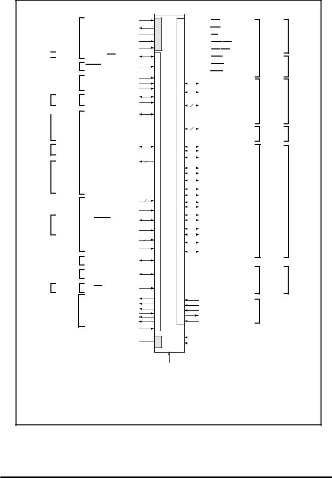
1 |
OVERVIEW |
1.3 Pin Function |
|
|
|
Port 7 
Port 22
Port 19 
Port 17
Port 15
Port 14
Port 13
Port 12
Port 21
Port 18
Port 16
Port 11
Port 10
Port 9
Port 6
Port 6
Clock
Reset
Mode
CAN
Multijunction timer
A-D converter
Port 6
Port 22
Interrupt controller
DBGUG
XIN
XOUT
VCNT
OSC-VCC
OSC-VSS
P70/BCLK/WR
RESET
MOD0
MOD1
FP
P220/CTX
P221/CRX
P190–P197/TIN26–TIN33 P172, P173/TIN24, TIN25 P150–P157/TIN0–TIN7 P140–P147/TIN8–TIN15 P130–P137/TIN16–TIN23
P124–P127/
TCLK0–TCLK 3
P210–P217/TO37–TO44
P180–P187/TO29–TO36
P160–P167/TO21–TO28
P110–P117/TO0–TO7
P100–P107/TO8–TO15
P93–P97/TO16–TO20
AD0IN0–AD0IN15
AD1IN0–AD1IN15
P67/ADTRG
AVCC0, AVCC1
AVSS0, AVSS1
AVREF0, AVREF1
P61–P63
P222, P223
P64/SBI
TRCLK
TRSYNC
TRDATA
JDBI
JEVENTO
JEVENT1
VCCE
VCCI
34
4
45
16
16
2
2
2
3
8
7
6
 3V.3
3V.3
 5V
5V
 3V.3
3V.3

 P45/CS1

 P44/CS0

 P43/RD

 P42/BHW/BHE

 P41/BLW/BLE

 P71/WAIT

 P72/HREQ

 P73/HACK
|
|
|
|
P224/A11 (Note2) |
|
|
|
|
|
|
|
|
|
P225/A12 (Note2) |
|
|
|
20 |
|
|
|
|
P20–P27/A23–A30 |
|
M32170F3 |
|
|
|
|
|
|
|
||
|
|
|
P30–P37/A15–A22 |
|
|
|
|
|
P46, P47/A13, A14 |
|
|
|
16 |
P00–P07/DB0–DB7 |
|
|
|
|
|
|
|
|
|
|
|
|
|
|
P10–P17/DB8–DB15 |
, |
VWG |
5V |
|
|
M32170F4VWG |
|
P82/TXD0 |
||
|
|
|
|
P83/RXD0 |
|
|
|
|
P84/SCLKI0/SCLKO0 |
|
|
|
|
|
|
|
|
|
P85/TXD1 |
|
|
|
|
|
|
|
|
|
P86/RXD1 |
|
|
|
|
|
|
|
|
|
P87/SCLKI1/SCLKO1 |
|
|
|
|
|
, |
|
|
|
P174/TXD2 |
|
|
|
||
|
|
|
P175/RXD2 |
|
M32170F6VWG |
|
|
|
|
|
|
|
||
|
|
|
P176/TXD3 |
|
|
|
|
|
|
|
|
|
|
P177/RXD3 |
|
|
|
|
|
|
|
|
|
P200/TXD4 |
|
|
|
|
|
|
|
|
|
P201/RXD4 |
|
|
|
|
|
|
|
|
|
P202/TXD5 |
|
|
|
|
|
|
|
|
|
P203/RXD5 |
|
|
|
|
P65/SCLKI4/SCLKO4 |
|
|
|
|
|
|
|
|
|
P66/SCLKI5/SCLKO5 |
|
|
|
|

 P74/RTDTXD

 P75/RTDRXD

 P76/RTDACK

 P77/RTDCLK
JTMS
JTCK
JTRST
JTDO
JTDI
3V.3 |
|
VDD |
|
||
|
FVCC |
|
|
||
|
|
|
 16
16
VSS
Note1. |
3.3V |
: denotes blocks operating with a 3.3 V power supply |
|
5V |
: denotes blocks operating with a 5 V power supply. |
Note2. Use caution when using this port because it has a debug event function.
Note3. 255FBGA is currently under development.
Figure 1.3.2 Pin Function Diagram of 255FBGA
Bus control
Address
bus
Data
bus
Serial
I/O
Real-time
debugger
JTAG
Port 4
Port 7
Port 22
Port 2
Port 3
Port 4
Port 0
Port 1
Port 6
Port 8
Port17
Port 20
Port 7
1-11 |
Ver.0.10 |

1 |
|
|
|
|
|
|
|
|
|
|
|
|
|
OVERVIEW |
|||
|
|
|
|
|
|
|
|
|
|
|
|
|
1.3 Pin Function |
||||
|
|
|
|
|
|
|
|
|
|
|
|
|
|
|
|||
|
Table 1.3.1 Description of the 32170 Pin Function (1/6) |
|
|
|
|
|
|
|
|||||||||
|
|
|
|
|
|
|
|
|
|
|
|
|
|
|
|
|
|
|
Type |
|
Pin Name |
Signal Name |
Input/Output |
Function |
|
|
|
|
|
|
|
||||
|
|
|
|
|
|
|
|
|
|
|
|
|
|
|
|
||
|
Power |
VCCE |
Power supply |
— |
Power supply to external I/O ports (5 V). |
|
|
|
|||||||||
|
supply |
|
|
|
|
|
|
|
|
|
|
|
|
|
|
|
|
|
VCCI |
Power supply |
— |
Power supply to internal logic (3.3 V). |
|
|
|
||||||||||
|
|
|
|
|
|||||||||||||
|
|
|
|
|
|
|
|
|
|
|
|
|
|
|
|||
|
|
VDD |
RAM power supply |
— |
Power supply for internal RAM backup (3.3 V). |
|
|
|
|||||||||
|
|
|
|
|
|
|
|
|
|
|
|
|
|
|
|||
|
|
FVCC |
FLASH power supply |
— |
Power supply for internal flash memory (3.3 V). |
|
|
|
|||||||||
|
|
|
|
|
|
|
|
|
|
|
|
|
|
|
|||
|
|
VSS |
Ground |
— |
Connect all VSS to ground (GND). |
|
|
|
|||||||||
|
|
|
|
|
|
|
|
|
|
|
|
|
|
|
|||
|
Clock |
|
XIN, |
Clock |
Input |
Clock input/output pins. These pins contains a PLL-based |
|||||||||||
|
|
XOUT |
|
Output |
frequency multiplier circuit. Apply a clock whose frequency |
||||||||||||
|
|
|
|
|
|
|
|
|
is 1/4 the operating frequency. (When using 40 MHz CPU |
||||||||
|
|
|
|
|
|
|
|
|
clock, XIN input = 10.0 MHz) |
|
|
|
|||||
|
|
|
|
|
|
|
|
|
|
|
|
|
|
|
|||
|
|
|
|
|
|
System clock |
Output |
This pin outputs a clock whose frequency is twice that of |
|||||||||
|
|
BCLK/WR |
|
||||||||||||||
|
|
|
|
|
|
|
|
|
external input clock. (When using 10 MHz external input |
||||||||
|
|
|
|
|
|
|
|
|
clock, BCLK output = 20 MHz). Use this output when |
||||||||
|
|
|
|
|
|
|
|
|
external operation needs to be synchronized. |
|
|
|
|||||
|
|
|
|
|
|
|
|
|
|
|
|
|
|
|
|||
|
|
OSC-VCC |
Power supply |
— |
Power supply for PLL circuit. Connect OSC-VCC to the |
||||||||||||
|
|
|
|
|
|
|
|
|
power supply rail. |
|
|
|
|
|
|||
|
|
|
|
|
|
|
|
|
|
|
|
|
|
|
|
||
|
|
OSC-VSS |
Ground |
— |
Connect OSC-VSS to ground. |
|
|
|
|||||||||
|
|
|
|
|
|
|
|
|
|
|
|
|
|
||||
|
|
VCNT |
PLL control |
Input |
This pin controls the PLL circuit. Connect a resistor and |
||||||||||||
|
|
|
|
|
|
|
|
|
capacitor to it. (For external circuits, refer to Section 18.1.1, |
||||||||
|
|
|
|
|
|
|
|
|
"Example of an Oscillator Circuit.") |
|
|
|
|||||
|
|
|
|
|
|
|
|
|
|
|
|
|
|
|
|||
|
Reset |
|
|
|
Reset |
Input |
This pin resets the internal circuit. |
|
|
|
|||||||
|
RESET |
|
|
|
|||||||||||||
|
|
|
|
|
|
|
|
|
|
|
|
|
|
|
|
||
|
Mode |
|
MOD0 |
Mode |
Input |
These pins set operation mode. |
|
|
|
||||||||
|
|
MOD1 |
|
|
|
MOD0 |
|
MOD1 |
|
Mode |
|
|
|
||||
|
|
|
|
|
|
|
|
|
|
||||||||
|
|
|
|
|
|
|
|
|
0 |
|
0 |
|
Single-chip mode |
|
|
|
|
|
|
|
|
|
|
|
|
|
0 |
|
1 |
|
Extended external mode |
||||
|
|
|
|
|
|
|
|
|
1 |
|
0 |
|
Processor mode |
|
|
|
|
|
|
|
|
|
|
|
|
|
|
|
|
|
|
(Boot mode) |
(Note) |
||
|
|
|
|
|
|
|
|
|
1 |
|
1 |
|
(Reserved) |
|
|
|
|
|
|
|
|
|
|
|
|
|
|
|
|
|
|
|
|
|
|
|
Address |
|
A11 – A30 |
Address |
Output |
The device has 20 address lines (A11-A30) to allow two |
|||||||||||
|
Bus |
|
|
|
|
|
Bus |
|
channels of up to 2 MB of memory space to be added |
||||||||
|
|
|
|
|
|
|
|
|
external to the chip. A31 is not output. |
|
|
|
|||||
|
|
|
|
|
|
|
|
|
|
|
|
|
|
|
|
|
|
Note: For boot mode, refer to Chapter 6, "Internal Memory."
1-12 |
Ver.0.10 |
Loading...