


CL-81

LCD TV
SERVICE MANUAL
CAUTION
BEFORE SERVICING THE CHASSIS,
READ THE SAFETY PRECAUTIONS IN THIS MANUAL.
CHASSIS : CL-81
MODEL : 15LC1RB-MG / 20LC1RB-MG
website:http://biz.LGservice.com
e-mail:http://www.LGEservice.com/techsup.html

- 2 -
CONTENTS
CONTENTS .............................................................................................. 2
PRODUCT SAFETY ..................................................................................3
DISASSEMBLY..........................................................................................6
SPECIFICATION........................................................................................7
ADJUSTMENT INSTRUCTION ...............................................................10
SVC REMOCON ......................................................................................13
TROUBLE SHOOTING............................................................................14
BLOCK DIAGRAM...................................................................................18
WIRING DIAGRAM..................................................................................20
EXPLODED VIEW .................................................................................. 21
REPLACEMENT PARTS LIST ............................................................... 23
SVC. SHEET ...............................................................................................
- 3 -
SAFETY PRECAUTIONS
Many electrical and mechanical parts in this chassis have special safety-related characteristics. These parts are identified by in the
Schematic Diagram and Replacement Parts List.
It is essential that these special safety parts should be replaced with the same components as recommended in this manual to prevent
Shock, Fire, or other Hazards.
Do not modify the original design without permission of manufacturer.
General Guidance
An isolation Transformer should always be used during the
servicing of a receiver whose chassis is not isolated from the AC
power line. Use a transformer of adequate power rating as this
protects the technician from accidents resulting in personal injury
from electrical shocks.
It will also protect the receiver and it's components from being
damaged by accidental shorts of the circuitry that may be
inadvertently introduced during the service operation.
If any fuse (or Fusible Resistor) in this TV receiver is blown,
replace it with the specified.
When replacing a high wattage resistor (Oxide Metal Film Resistor,
over 1W), keep the resistor 10mm away from PCB.
Keep wires away from high voltage or high temperature parts.
Before returning the receiver to the customer,
always perform an AC leakage current check on the exposed
metallic parts of the cabinet, such as antennas, terminals, etc., to
be sure the set is safe to operate without damage of electrical
shock.
Leakage Current Cold Check(Antenna Cold Check)
With the instrument AC plug removed from AC source, connect an
electrical jumper across the two AC plug prongs. Place the AC
switch in the on position, connect one lead of ohm-meter to the AC
plug prongs tied together and touch other ohm-meter lead in turn to
each exposed metallic parts such as antenna terminals, phone
jacks, etc.
If the exposed metallic part has a return path to the chassis, the
measured resistance should be between 1MΩ and 5.2MΩ.
When the exposed metal has no return path to the chassis the
reading must be infinite.
An other abnormality exists that must be corrected before the
receiver is returned to the customer.
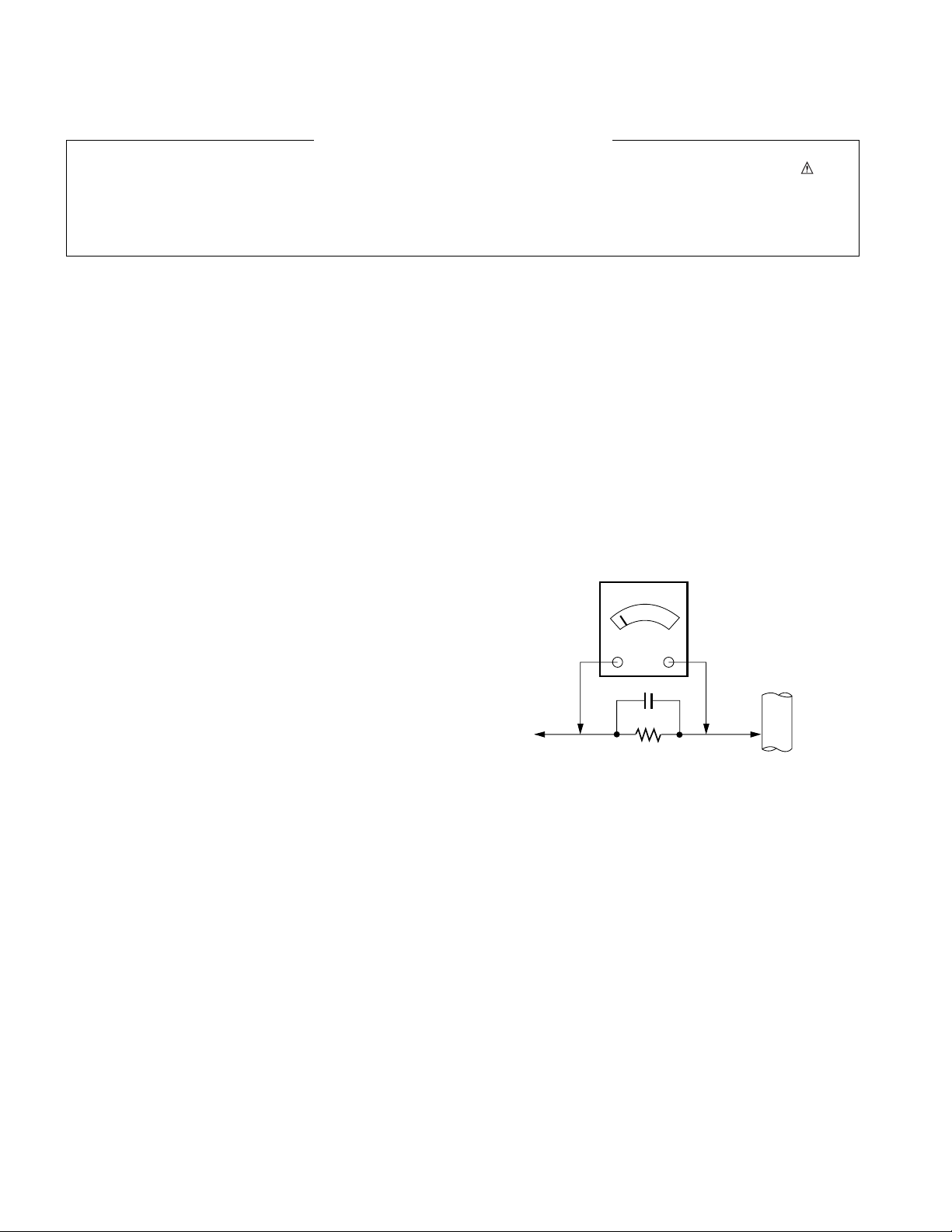
Leakage Current Hot Check (See below Figure)
Plug the AC cord directly into the AC outlet.
Do not use a line Isolation Transformer during this check.
Connect 1.5K/10watt resistor in parallel with a 0.15uF capacitor
between a known good earth ground (Water Pipe, Conduit, etc.)
and the exposed metallic parts.
Measure the AC voltage across the resistor using AC voltmeter
with 1000 ohms/volt or more sensitivity.
Reverse plug the AC cord into the AC outlet and repeat AC voltage
measurements for each exposed metallic part. Any voltage
measured must not exceed 0.75 volt RMS which is corresponds to
0.5mA.
In case any measurement is out of the limits specified, there is
possibility of shock hazard and the set must be checked and
repaired before it is returned to the customer.
Leakage Current Hot Check circuit
IMPORTANT SAFETY NOTICE
0.15uF
To Instrument's
exposed
METALLIC PARTS
AC Volt-meter
Good Earth Ground
such as WATER PIPE,
CONDUIT etc.
1.5 Kohm/10W

- 4 -
CAUTION: Before servicing receivers covered by this service
manual and its supplements and addenda, read and follow the
SAFETY PRECAUTIONS on page 3 of this publication.
NOTE: If unforeseen circumstances create conflict between the
following servicing precautions and any of the safety precautions on
page 3 of this publication, always follow the safety precautions.
Remember: Safety First.
General Servicing Precautions
1. Always unplug the receiver AC power cord from the AC power
source before;
a. Removing or reinstalling any component, circuit board
module or any other receiver assembly.
b. Disconnecting or reconnecting any receiver electrical plug or
other electrical connection.
c. Connecting a test substitute in parallel with an electrolytic
capacitor in the receiver.
CAUTION: A wrong part substitution or incorrect polarity
installation of electrolytic capacitors may result in an
explosion hazard.
2. Test high voltage only by measuring it with an appropriate high
voltage meter or other voltage measuring device (DVM,
FETVOM, etc) equipped with a suitable high voltage probe.
Do not test high voltage by "drawing an arc".
3. Do not spray chemicals on or near this receiver or any of its
assemblies.
4. Unless specified otherwise in this service manual, clean
electrical contacts only by applying the following mixture to the
contacts with a pipe cleaner, cotton-tipped stick or comparable
non-abrasive applicator; 10% (by volume) Acetone and 90% (by
volume) isopropyl alcohol (90%-99% strength)
CAUTION: This is a flammable mixture.
Unless specified otherwise in this service manual, lubrication of
contacts in not required.
5. Do not defeat any plug/socket B+ voltage interlocks with which
receivers covered by this service manual might be equipped.
6. Do not apply AC power to this instrument and/or any of its
electrical assemblies unless all solid-state device heat sinks are
correctly installed.
7. Always connect the test receiver ground lead to the receiver
chassis ground before connecting the test receiver positive
lead.
Always remove the test receiver ground lead last.
8. Use with this receiver only the test fixtures specified in this
service manual.
CAUTION: Do not connect the test fixture ground strap to any
heat sink in this receiver.
Electrostatically Sensitive (ES) Devices
Some semiconductor (solid-state) devices can be damaged easily
by static electricity. Such components commonly are called
Electrostatically Sensitive (ES) Devices. Examples of typical ES
devices are integrated circuits and some field-effect transistors and
semiconductor "chip" components. The following techniques
should be used to help reduce the incidence of component
damage caused by static by static electricity.
1. Immediately before handling any semiconductor component or
semiconductor-equipped assembly, drain off any electrostatic
charge on your body by touching a known earth ground.
Alternatively, obtain and wear a commercially available
discharging wrist strap device, which should be removed to
prevent potential shock reasons prior to applying power to the
unit under test.
2. After removing an electrical assembly equipped with ES
devices, place the assembly on a conductive surface such as
aluminum foil, to prevent electrostatic charge buildup or
exposure of the assembly.
3. Use only a grounded-tip soldering iron to solder or unsolder ES
devices.
4. Use only an anti-static type solder removal device. Some solder
removal devices not classified as "anti-static" can generate
electrical charges sufficient to damage ES devices.
5. Do not use freon-propelled chemicals. These can generate
electrical charges sufficient to damage ES devices.
6. Do not remove a replacement ES device from its protective
package until immediately before you are ready to install it.
(Most replacement ES devices are packaged with leads
electrically shorted together by conductive foam, aluminum foil
or comparable conductive material).
7. Immediately before removing the protective material from the
leads of a replacement ES device, touch the protective material
to the chassis or circuit assembly into which the device will be
installed.
CAUTION: Be sure no power is applied to the chassis or circuit,
and observe all other safety precautions.
8. Minimize bodily motions when handling unpackaged
replacement ES devices. (Otherwise harmless motion such as
the brushing together of your clothes fabric or the lifting of your
foot from a carpeted floor can generate static electricity
sufficient to damage an ES device.)
General Soldering Guidelines
1. Use a grounded-tip, low-wattage soldering iron and appropriate
tip size and shape that will maintain tip temperature within the
range or 500
o
F to 600oF.
2. Use an appropriate gauge of RMA resin-core solder composed
of 60 parts tin/40 parts lead.
3. Keep the soldering iron tip clean and well tinned.
4. Thoroughly clean the surfaces to be soldered. Use a mall wirebristle (0.5 inch, or 1.25cm) brush with a metal handle.
Do not use freon-propelled spray-on cleaners.
5. Use the following unsoldering technique
a. Allow the soldering iron tip to reach normal temperature.
(500
o
F to 600oF)
b. Heat the component lead until the solder melts.
c. Quickly draw the melted solder with an anti-static, suction-
type solder removal device or with solder braid.
CAUTION: Work quickly to avoid overheating the
circuitboard printed foil.
6. Use the following soldering technique.
a. Allow the soldering iron tip to reach a normal temperature
(500
o
F to 600oF)
b. First, hold the soldering iron tip and solder the strand against
the component lead until the solder melts.
c. Quickly move the soldering iron tip to the junction of the
component lead and the printed circuit foil, and hold it there
only until the solder flows onto and around both the
component lead and the foil.
CAUTION: Work quickly to avoid overheating the circuit
board printed foil.
d. Closely inspect the solder area and remove any excess or
splashed solder with a small wire-bristle brush.
SERVICING PRECAUTIONS

- 5 -
IC Remove/Replacement
Some chassis circuit boards have slotted holes (oblong) through
which the IC leads are inserted and then bent flat against the
circuit foil. When holes are the slotted type, the following technique
should be used to remove and replace the IC. When working with
boards using the familiar round hole, use the standard technique
as outlined in paragraphs 5 and 6 above.
Removal
1. Desolder and straighten each IC lead in one operation by gently
prying up on the lead with the soldering iron tip as the solder
melts.
2. Draw away the melted solder with an anti-static suction-type
solder removal device (or with solder braid) before removing the
IC.
Replacement
1. Carefully insert the replacement IC in the circuit board.
2. Carefully bend each IC lead against the circuit foil pad and
solder it.
3. Clean the soldered areas with a small wire-bristle brush.
(It is not necessary to reapply acrylic coating to the areas).
"Small-Signal" Discrete Transistor
Removal/Replacement
1. Remove the defective transistor by clipping its leads as close as
possible to the component body.
2. Bend into a "U" shape the end of each of three leads remaining
on the circuit board.
3. Bend into a "U" shape the replacement transistor leads.
4. Connect the replacement transistor leads to the corresponding
leads extending from the circuit board and crimp the "U" with
long nose pliers to insure metal to metal contact then solder
each connection.
Power Output, Transistor Device
Removal/Replacement
1. Heat and remove all solder from around the transistor leads.
2. Remove the heat sink mounting screw (if so equipped).
3. Carefully remove the transistor from the heat sink of the circuit
board.
4. Insert new transistor in the circuit board.
5. Solder each transistor lead, and clip off excess lead.
6. Replace heat sink.
Diode Removal/Replacement
1. Remove defective diode by clipping its leads as close as
possible to diode body.
2. Bend the two remaining leads perpendicular y to the circuit
board.
3. Observing diode polarity, wrap each lead of the new diode
around the corresponding lead on the circuit board.
4. Securely crimp each connection and solder it.
5. Inspect (on the circuit board copper side) the solder joints of
the two "original" leads. If they are not shiny, reheat them and if
necessary, apply additional solder.
Fuse and Conventional Resistor
Removal/Replacement
1. Clip each fuse or resistor lead at top of the circuit board hollow
stake.
2. Securely crimp the leads of replacement component around
notch at stake top.
3. Solder the connections.
CAUTION: Maintain original spacing between the replaced
component and adjacent components and the circuit board to
prevent excessive component temperatures.
Circuit Board Foil Repair
Excessive heat applied to the copper foil of any printed circuit
board will weaken the adhesive that bonds the foil to the circuit
board causing the foil to separate from or "lift-off" the board. The
following guidelines and procedures should be followed whenever
this condition is encountered.
At IC Connections
To repair a defective copper pattern at IC connections use the
following procedure to install a jumper wire on the copper pattern
side of the circuit board. (Use this technique only on IC
connections).
1. Carefully remove the damaged copper pattern with a sharp
knife. (Remove only as much copper as absolutely necessary).
2. carefully scratch away the solder resist and acrylic coating (if
used) from the end of the remaining copper pattern.
3. Bend a small "U" in one end of a small gauge jumper wire and
carefully crimp it around the IC pin. Solder the IC connection.
4. Route the jumper wire along the path of the out-away copper
pattern and let it overlap the previously scraped end of the good
copper pattern. Solder the overlapped area and clip off any
excess jumper wire.
At Other Connections
Use the following technique to repair the defective copper pattern
at connections other than IC Pins. This technique involves the
installation of a jumper wire on the component side of the circuit
board.
1. Remove the defective copper pattern with a sharp knife.
Remove at least 1/4 inch of copper, to ensure that a hazardous
condition will not exist if the jumper wire opens.
2. Trace along the copper pattern from both sides of the pattern
break and locate the nearest component that is directly
connected to the affected copper pattern.
3. Connect insulated 20-gauge jumper wire from the lead of the
nearest component on one side of the pattern break to the lead
of the nearest component on the other side.
Carefully crimp and solder the connections.
CAUTION: Be sure the insulated jumper wire is dressed so the
it does not touch components or sharp edges.
- 6 -
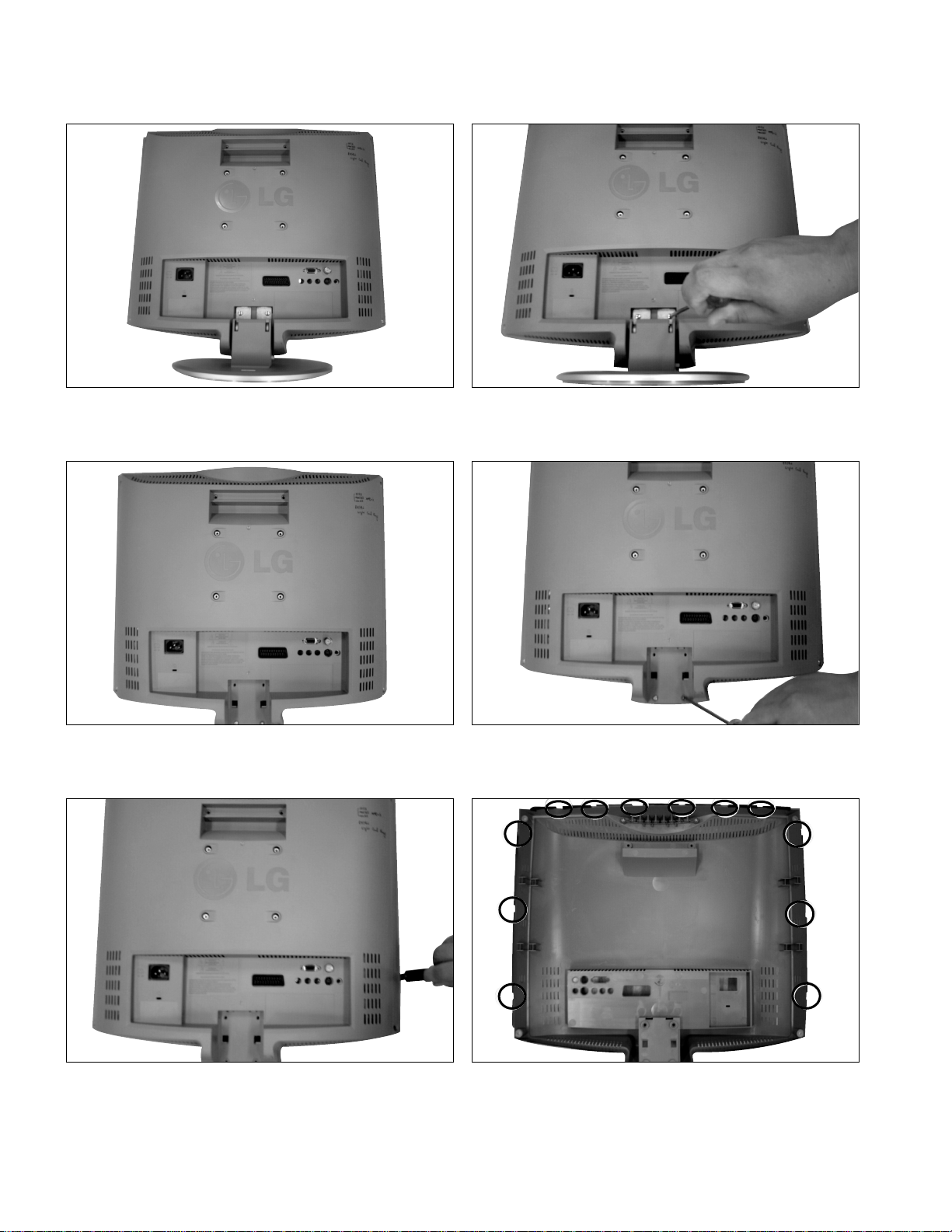
DISASSEMBLY
#1 #2 Detached stand assy (Remove the screws)
#3 Disassembly stand assy #4 Detached Backcover (Remove the screw)
#5 Open the Backcover's latch with jig #6 Unlock latch between Cabinet and Backcover
- 7 -
SPECIFICATION
1. Application range
This specification is applied to CL-81 chassis.
2. Requirement for Test
Testing for standard of each part must be followed in below
condition.
(1) Temperature: 25°C ± 2°C
(2) Humidity: 65% ± 10%
(3) Power: Standard input voltage (AC 100-240V, 50/60Hz)
(4) Measurement must be performed after heat-run more than
30min.
(5) Adjusting standard for this chassis is followed a special
standard.
3.General Specification
3-1. 15LC1R
4. Mechanical Specification
No.
Item
Specification Remark
1
TFT Color LCD Module
20.1 inches(510.54mm) diagonal
0.2125mm(H)x0.6375mm(V)xRGB
TTL
8BIT, 16,777,216 colors
432(H) x 331.5(V) x 25(D)
Anti-Glare, Hard Coating(3H)
Normally Black
6 CCFL(6 lamps)
25ms(R.T.:12ms + F.T.:13ms)
LPL
NOTE : Specifications and others are subject to change without notice for improvement
.
No.
1 Product 15LC1R/20LC1R
Dimension Width(W) Lengh(D) Height(H)
Before Packing 377.6/492.4 242.8/272.8 394.5/483.3
After Packing 433/574.0 143/225.0 442/627.0
2 Product Only SET 5.6Kg/8.7Kg
Weight With BOX 7.7Kg/11.1Kg
Type
ActiveDisplay Area
Pixel Pitch [mm]
Electrical Interface
Color Depth
Size [mm]
Surface Treatment
Operating Mode
Back light Unit
R/T Typ.
Item
Content
Remark
No.
Item
Specification Remark
1
TFT Color LCD Module
15.0 inches(380.16mm) diagonal(Aspect 4:3)
0.297mm(H)x0.297mm(V)xRGB
LVDS
6BIT, 16,777,216 colors
332.8(H) x 262.2(V) x 18(D)
Anti-Glare(HAZE 3%), Hard Coating(3H)
Normally Black
4 CCFL(4 lamps)
R.T.:5ms + F.T.:11ms(Typ)
LPL
Type
ActiveDisplay Area
Pixel Pitch [mm]
Electrical Interface
Color Depth
Size [mm]
Surface Treatment
Operating Mode
Back light Unit
R/T Typ.
3-2. 20LC1R
- 8 -
6.Optical Character
6-1. 15LC1R
5. Reference table-Function
No.
Item
Specification
Remark
1 Teletext TOP, FLOF NO
2 REMOCON NEC Code NTSC
3 AV Input 1 Rear
4 S-Video Input 1 Rear
5 Component Input 1 Rear
6 PERI TV Connector Full SCART : 0 NO
7 Ear-phone output 1 Rear
8 2 Carrier Stereo X
9 NICAM Stereo X
10 2 Carrier Daul X
11 NICAM Daul X
12 DW(Double Window) Mode X
13 MW(Multi Window) Mode X
14 Film Mode X
15 Noise Reduction X
16 Progressive Scan O
17 Motion Detection X
18 SRS WOW X
19 Swivel Speaker X
20 EZ-pip X
21 ARC X
22 DRP X
23 DCDI X
24 HDCP X
Item
Remark
Specification
Viewing Angle
<CR
≥
10>
Luminance
Contrast Ratio
CIE Color Coordinates
All White/All Black
In PC input
Contrast 100/Brightness 50
In AV Input
PSM : Dynamic
White
(100 IRE)
R/L,
U/D
Luminance(cd/
)
Variation
CR
Typ
65/65
45/55
400
400
0.283
0.298
0.313
0.329
0.283
0.298
0.274
0.286
Min
55/55
40/50
300
300
0.253
0.268
0.283
0.299
0.253
0.268
0.244
0.256
WHITE
(Normal)
WHITE
(Warm)
WHITE
(Normal)
WHITE
(Cool)
Wx
Wy
Wx
Wy
Wx
Wy
Wx
Wy
Max
1.3
0.313
0.328
0.343
0.359
0.313
0.328
0.304
0.316
No.
1
2
3
4
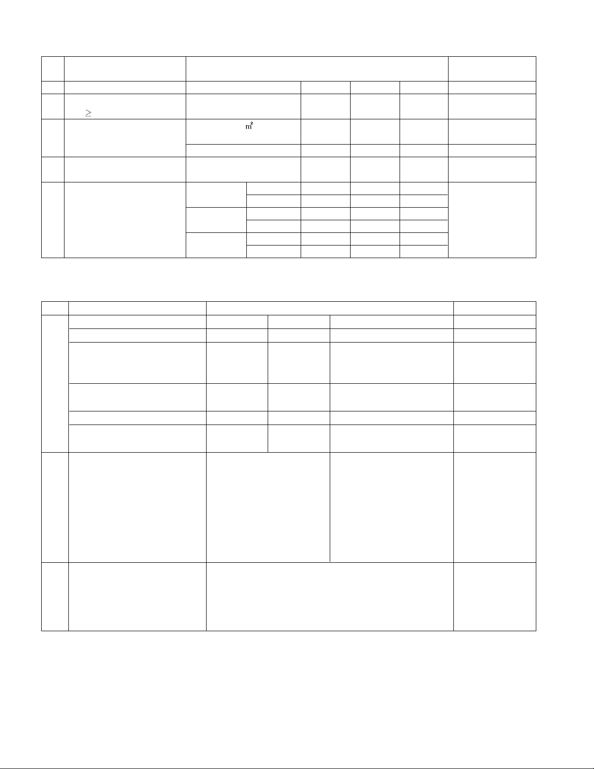
- 9 -
7-1.General Specification
7.Engineering Specification
No Item Specification Remark
1 ENERGE-15LC1R SYNC(V/H) VIDEO POWER CONSUMPTION LED COLOE
Normal-15LC1R On/On Active ≤ 40W BLUE
Sleep Mode-15LC1R Off/On
(PC Mode) On/Off Off ≤ 1W Amber
Off/Off
Off Mode-15LC1R Off ≤ 1W Off(PC)
Amber(TV/AV)
Normal-20LC1R On/On Active ≤ 65W BLUE
Off Misw-20LC1R Off/Off Off ≤ 1W(110V) Orange
≤ 1W(220V)
2 D-SUB 1 : RED 2 : GREEN 10 : DIGITAL GND
Pin configuration 3 : BLUE 4 : ID2 (GND)
5 : S.T (GND) 6 : RED
7 : GREEN GND 8 : BLUE GND
9 : N.C 10 : D-GND
11 : ID0(GND) 12 : SDA
13 : H-SYNC 14 : V-SYNC
15 : SCL SHELL : GND
3 Control Functin 1) Contrast / Brightness
2) H-Position
3) Tracking : Clock / Phase
4) Auto Configure
5) Reset
Item RemarkSpecification
Viewing Angle
<CR
10>
Luminance
Contrast Ratio
CIE Color Coordinates
All White/All Black
In AV Input
PSM : Dynamic
White
(100 IRE)
R/L,
U/D
Luminance(cd/
)
Variation
CR
Typ
88/88
88/88
40
350
0.313
0.329
0.283
0.298
0.274
0.286
Min
85/85
85/85
300
250
0.283
0.299
0.253
0.268
0.244
0.256
WHITE
(Warm)
WHITE
(Normal)
WHITE
(Cool)
Wx
Wy
Wx
Wy
Wx
Wy
Max
1.3
0.343
0.359
0.313
0.328
0.304
0.316
No.
1
2
3
4
6-2. 20LC1R

- 10 -
1. Application
This document is applied to 15", 20" LCD TV which is
manufactured in Monitor Factory or is produced on the basis
of this data.
2. Designation
2.1 The adjustment is according to the order which is
designated and which must be followed, according to the
plan which can be changed only on agreeing.
2.2. Power Adjustment: Free Voltage
2.3. Magnetic Field Condition: Nil.
2.4. Input signal Unit: Product Specification Standard
2.5. Reserve after operation: Above 30 Minutes
2.6. Adjustment equipments: Pattern Generator (MSPG-925
or Equivalent), DDC Adjustment Jig equipment, SVC
remote controller
3. Adjustment
3.1 APC
After Manual-Insult, executing APC
3.2 ISP UOC file
3.2.1 Required Equipment
- JIG for ISP
- PC that is installed with "WISP" program.
- Control + Power LED PCB Ass'y
3.2.2 ISP Sequence
1) Connect main board with JIG for ISP
2) Execute "WISP" Program.
3) Compare UOC version in BOM with version of hex file.
4) Push "Brouse..." button and select hex file.
5) Push " Auto Execute" button.
6) Occur an Error, push "Erase" button and try again and
again. 2)~5)
7) After finishing ISP, Must AC off / ON
8) Wait LED is not blink anymore
3.3 ADC Process
"IIC_ SW" must set "0"(After ISP, automatically set "0")
3.3.1 AV(CVBS) Mode Adjustment
3.3.1.1 Auto Gain/Offset Adjustment
Select AV(Video) in Input menu
Signal equipment : MSPG925
Output Jack : CVBS
Output Voltage : 700 mVp-p (patt # 29 in MSPG925)
Resolution : NTSC J - 720 x 480 @59,94Hz (Model
#207 in MSPG925)
Adjust by commanding AUTO_COLOR_ADJUST
(0xF1) 0x00 0x00 instruction.
3.3.1.2 Confirmation of adjustment process
We confirm whether "0x01" address of EEPROM
"0xA0" is "0xAA" or not.
If "0x01" address of EEPROM "0xA0" isn't "0xAA", we
adjust once more in adjustment line by adjust method
of 3.2.1.2.
We can confirm the ADC values from "0x0C~0x11"
addresses in a page "0xA0"
3.3.2 Component Mode Adjustment
3.3.2.1 Auto Gain/Offset Adjustment
Select Component in Input menu
Signal equipment : MSPG925
Output Jack : D4(Japan) or Componen(Except Japan)
Output Voltage : 700 mVp-p (patt # 8 in MSPG925)
Resolution 483/60P - 720 x 483p @59.94Hz (Model
#212 in MSPG925)
Adjust by commanding AUTO_COLOR_ADJUST
(0xF1) 0x00 0x00 instruction.
3.3.2.2 Confirmation of adjustment process
We confirm whether "0x01" address of EEPROM
"0xA0" is "0xAA" or not.
If "0x01" address of EEPROM "0xA0" isn't "0xAA", we
adjust once more in adjustment line by adjust method
of 3.2.1.2.
We can confirm the ADC values from "0x??~0x??"
addresses in a page "0xA0"
*Caution*
If DDC CMD don't work, please check below.
1. Enter SVC menu by SVC Remote controller
2. Enter "ETC" menu
Check please, IIC_SW is "0" or "1".
- IIC_SW "0" : DDC Communications.(DDC2AB)
- IIC_SW "1" : EDID Write/Read (DDC2B) and Factory
default.
3.4 Function Check
3.4.1 Check display and sound
"IIC_ SW" must set "1"
Check Input and Signal items. (cf. work instructions)
1. TV
2. AV (CVBS/ S-Video)
3 Component
4. H/P Out
3.4.2 DCXO setting
: After finished all function check, "IIC_ SW" must set "0" by
pushing "TILT" key in SVC remocon
ADJUSTMENT INSTRUCTION

- 11 -
4. Total Assembly line process
4.1 Adjustment Preparation
"IIC_ SW" must set "0"
Above 30 minutes H/run in RF no signal
15 Pin D-Sub Jack is connected to the signal of
Pattern Generator.
4.2 Confirmation of Luminance
Set Statement
Input : CVBS
Contrast : 100(Max)
Brightness : 50
CSM : Normal
Signal equipment displays
Output Voltage : 700 mVp-p
Output Mode : Full White pattern (100 IRE)
Confirm whether luminance is over 300cd or not
4.3 Confirmation of Color Coordinate
Input Full White Pattern
Set CSM : Normal (9300K)
Confirm whether x = 0.283±0.03, y=0.298±0.03 or not
Set CSM : Warm (6500K)
Confirm whether color coordinate is x= 0.313±0.03,
y=0.329±0.03 or not
Set CSM : Warm (11000K)
Confirm whether color coordinate is x= 0.274±0.03,
y=0.286±0.03 or not
After confirming Color coordinates, Must return to
Normal
* After Confirming color coordinate and luminance, "IIC_ SW"
must set "1"
 Loading...