

Page 1

Training Manual
50PJ350 Plasma Display
50PJ350 Plasma Display
Advanced Single Scan Troubleshooting
50" Class HD 720p Plasma TV
(50" diagonally)
Published July 12th, 2010
Updated August 12
th
, 2010
Page 2

OUTLINE
OUTLINE
Preliminary:
Contact Information, Preliminary Matters, Specifications,
Plasma Overview, General Troubleshooting Steps,
Disassembly Instructions, Voltage and Signal Distribution
Overview of Topics to be Discussed
Troubleshooting:
Circuit Board Operation, Troubleshooting and Alignment of :
• Switch Mode Power Supply
• Y-SUS Board Delivers Logic Signals and FG5V to lower Y-Drive board.
• Y-Drive Boards (1 Upper and 1 Lower).
Lower can run separately, but you MUST remove the Upper completely.
• Z-SUS Output Board (Also uses one Z-SUB board for bottom panel connector)
• Control Board
• X Drive Boards (3)
• Main Board
• Interconnect Diagram: 11X17 Foldout Section used as a quick reference sheet.
• No Main Power Switch (Vacation Switch).
No VS On command input to SMPS
2
July 2010 50PJ350 Plasma
Page 3

Overview of Topics to be Discussed
Overview of Topics to be Discussed
50PJ350 Plasma Display
The first section will cover Contact Information and Important Safety Precautions
for the Customers Safety as well as the Technician and the Equipment.
Basic Troubleshooting Techniques which can save time and money sometimes
can be overlooked. These techniques will also be presented.
The next section will get the Technician familiar with the Disassembly, Identification
and Layout of the Plasma Display Panel.
At the end of this Section the Technician should be able to Identify the Circuit
Boards and have the ability and knowledge necessary to safely remove and
replace any Circuit Board or Assembly.
3
July 2010 50PJ350 Plasma
Page 4
LG Contact Information
LG Contact Information
Customer Service (and Part Sales) (800) 243-0000
Technical Support (and Part Sales) (800) 847-7597
USA Website (GSFS) http://gsfs-america.lge.com
Customer Service Website us.lgservice.com
Knowledgebase Website lgtechassist.com
LG Web Training lge.webex.com
LG CS Academy lgcsacademy.com
LCD-DV:
PLASMA:
PDP Panel Alignment Handbook, Schematics with Bookmarks
32LG40, 32LH30, 37LH55, 42LG60, 42LG70, 42LH20, 42LH40, 42LH50, 42LH90, 42SL80,
47LG90, 47LH85, 47LE8500
42PG20, 42PQ20, 42PQ30, 50PG20, 50PJ350, 50PK750, 50PS80, 50PS60, 60PK750,
60PS11, 60PS60, 60PS80
Also available on the Plasma Page:
Plasma Control Board ROM Update (Jig required)
Published July 2010 by LG Technical Support and Training
LG Electronics Alabama, Inc.
201 James Record Road, Huntsville, AL, 35813.
New: Software Downloads
Technical Assistance
Presentations with Audio/Video
and Screen Marks
http://136.166.4.200
New Training Materials on
New Training Materials on
the Learning Academy site
the Learning Academy site
4
July 2010 50PJ350 Plasma
Page 5

Preliminary Matters (The Fine Print)
Preliminary Matters (The Fine Print)
IMPORTANT SAFETY NOTICE
IMPORTANT SAFETY NOTICE
The information in this training manual is intended for use by persons possessing an adequate
background in electrical equipment, electronic devices, and mechanical systems. In any attempt
to repair a major Product, personal injury and property damage can result. The manufacturer or
seller maintains no liability for the interpretation of this information, nor can it assume any
liability in conjunction with its use. When servicing this product, under no circumstances should
the original design be modified or altered without permission from LG Electronics. Unauthorized
modifications will not only void the warranty, but may lead to property damage or user injury.
If wires, screws, clips, straps, nuts, or washers used to complete a ground path are removed for
service, they must be returned to their original positions and properly fastened.
CAUTION
CAUTION
To avoid personal injury, disconnect the power before servicing this product. If electrical power
is required for diagnosis or test purposes, disconnect the power immediately after performing
the necessary checks. Also be aware that many household products present a weight hazard.
At least two people should be involved in the installation or servicing of such devices.
Failure to consider the weight of an product could result in physical injury.
5
July 2010 50PJ350 Plasma
Page 6

(Electrostatic Static Discharge)
ESD Notice
ESD Notice
Today’s sophisticated electronics are electrostatic discharge (ESD) sensitive. ESD can weaken or damage
the electronics in a manner that renders them inoperative or reduces the time until their next failure.
Connect an ESD wrist strap to a ground connection point or unpainted metal in the product. Alternatively,
you can touch your finger repeatedly to a ground connection point or unpainted metal in the product. Before
removing a replacement part from its package, touch the anti-static bag to a ground connection point or
unpainted metal in the product. Handle the electronic control
repackaging a failed electronic control assembly in an anti-static bag, observe these same precautions.
Regulatory Information
Regulatory Information
This equipment has been tested and found to comply with the limits for a Class B digital device, pursuant to
Part 15 of the FCC Rules. These limits are designed to provide reasonable protection against harmful
interference when the equipment is operated in a residential installation. This equipment generates, uses,
and can radiate radio frequency energy, and, if not installed and used in accordance with the instruction
manual, may cause harmful interference to radio communications. However, there is no guarantee that
interference will not occur in a particular installation. If this equipment does cause harmful interference to
radio or television reception, which can be determined by turning the equipment off and on, the user is
encouraged to try to correct the interference by one or more of the following measures: Reorient or relocate
the receiving antenna; Increase the separation between the equipment and the receiver; Connect the
equipment to an outlet on a different circuit than that to which the receiver is connected; or consult the
dealer or an experienced radio/TV technician for help.
(Electrostatic Static Discharge)
assembly by its edges only. When
6
July 2010 50PJ350 Plasma
Page 7

Safety and Handling, Checking Points
Safety and Handling, Checking Points
Safety & Handling Regulations
1. Approximately 10 minute pre-run time is required before any adjustments are performed.
2. Refer to the Voltage Sticker inside the Panel when making adjustments on the Power Supply, Y-SUS and Z-SUS Boards.
3. Always adjust to the specified voltage level (+/- ½ volt) unless otherwise specified.
4. Be cautious of electric shock from the PDP module since the PDP module uses high voltage, check that the Power Supply
and Drive Circuits are completely discharged because of residual current stored before Circuit Board removal.
4. C-MOS circuits are used extensively for processing the Drive Signals and should be protected from static electricity.
5. The PDP Module must be carried by two people. Always carry vertical NOT horizontal.
6. The Plasma television should be transported vertically NOT horizontally.
7. Exercise care when making voltage and waveform checks to prevent costly short circuits from damaging the unit.
8. Be cautious of lost screws and other metal objects to prevent a possible short in the circuitry.
9. New Panels and Frames are much thinner than previous models. Be Careful with flexing these panels. Be careful
with lifting Panels from a horizontal position. Damage to the Frame mounts or panel can occur.
10. New Plasma models have much thinner cabinet assemblies and mounts.
Be extremely careful when moving the set around as damage can occur.
Checking Points to be Considered
1. Check the appearance of the Replacement Panel and Circuit Boards for both physical damage and part number accuracy.
2. Check the model label. Verify model names and board model matches.
3. Check details of defective condition and history. Example: Y-SUS or Y-Drive Board Failure, Mal-discharge on screen, etc.
7
July 2010 50PJ350 Plasma
Page 8

Basic Troubleshooting Steps
Basic Troubleshooting Steps
Define, Localize, Isolate and Correct
• Define
failure. Use your senses Sight, Smell, Touch and Hearing. Look for burned parts and check
for possible overheated components. Capacitors will sometimes leak dielectric material and
give off a distinct odor. Frequency of power supplies will change with the load, or listen for
relay closing etc. Observation of the front Power LEDs may give some clues.
• Localize
and after giving a thorough examination using your senses the first check should always be
the DC Supply Voltages to those circuits under test. Always confirm the supplies are not
only the proper level but be sure they are noise free. If the supplies are missing check the
resistance for possible short circuits.
• Isolate
Oscilloscope to make a final determination of the failure. Look for correct Amplitude
Phasing and Timing of the signals also check for the proper Duty Cycle of the signals.
Sometimes “glitches” or “road bumps” will be an indication of an imminent failure.
Look at the symptom carefully and determine what circuits could be causing the
After carefully checking the symptom and determining the circuits to be checked
To further isolate the failure, check for the proper waveforms with the
• Correct
check the DC Supplies for proper levels. Make all necessary adjustments and lastly always
perform a Safety AC Leakage Test before returning the product back to the Customer.
The final step is to correct the problem. Be careful of ESD and make sure to
8
July 2010 50PJ350 Plasma
Page 9

50PJ350 PRODUCT INFORMATION SECTION
50PJ350 PRODUCT INFORMATION SECTION
This section of the manual will discuss the specifications of the
50PJ350 Advanced Single Scan Plasma Display Television.
9
July 2010 50PJ350 Plasma
Page 10
50PJ350 Specifications
50PJ350 Specifications
50" Class (50" diagonal)
• 600Hz Sub Field Driving
• High Definition Resolution
1080P PLASMA HDTV
• 3M:1 Dynamic Contrast Ratio
• TruSlim Frame
• Picture Wizard II (Easy Picture Calibration)
• Smart Energy Saving
• Intelligent Sensor
• Dual XD™ Engine
• AV Mode(Cinema, Sports, Game)
• Clear Voice II
• ISFccc® Ready
• 24P Real Cinema
• USB 2.0 (JPEG, MP3)
• 3 HDMI™ 1.3 Inputs
• SIMPLINK™ Connectivity
For Full Specifications
See the Specification Sheet
• Dolby® Digital 5.1 Decoder
• Infinite Sound
10
July 2010 50PJ350 Plasma
Page 11

50PJ350 Logo Familiarization Page 1 of 3
50PJ350 Logo Familiarization Page 1 of 3
600Hz Sub Field Firing:
Capture every moment. Tired of streaky action or unclear plays during the
game? See sports, fast action and video games like never before. The 600Hz
refresh rate virtually eliminates motion blur.
3.000,000 : 1 Contrast Ratio
Stunning detail. No more worrying about dark scenes or dull colors.
The Mega Contrast ratio of 3,000,000:1 delivers more stunning colors and
deeper blacks than you can imagine.
TruSlim Design:
At less than 1" thick the new TruSlim Frame trims away distraction without
compromising screen size.
USB 2.0:
View videos and photos and listen to music on your TV through USB 2.0.
11
July 2010 50PJ350 Plasma
Page 12

50PJ350 Logo Familiarization Page 2 of 3
50PJ350 Logo Familiarization Page 2 of 3
HD RESOLUTION 720P HD Resolution Pixels: 1365 (H) × 768 (V)
See and experience more. Pictures are sharper.
Colors are more vibrant. Entertainment is more real.
Everything looks better on an HDTV.
HDMI (1.3 Deep Color) Digital multi-connectivity
HDMI (1.3 Deep color) provides a wider bandwidth (340MHz,
10.2Gbps) than that of HDMI 1.2, delivering a broader range of colors,
and also drastically improves the data-transmission speed.
Invisible Speaker
Personally tuned by Mr. Mark Levinson for LG
TAKE IT TO THE EDGE newly introduces ‘Invisible Speaker’ system,
guaranteeing first class audio quality personally tuned by Mr. Mark
Levinson, world renowned as an audio authority. It provides Full Sweet
Spot and realistic sound equal to that of theaters with its Invisible
Speaker.
Dual XD Engine
Realizing optimal quality for all images
One XD Engine optimizes the images from RF signals as another XD
Engine optimizes them from External inputs. Dual XD Engine presents
images with optimal quality two times higher than those of previous
models.
12
July 2010 50PJ350 Plasma
Page 13

50PJ350 Logo Familiarization Page 3 of 3
50PJ350 Logo Familiarization Page 3 of 3
AV Mode "One click" Cinema, Sports, Game mode.
AV Mode is three preset picture and audio settings. It allows the viewer
to quickly switch between common settings. It includes Cinema, Sports,
and Game Modes.
Clear Voice Clearer dialogue sound
Automatically enhances and amplifies the sound of the human voice
frequency range to provide high-quality dialogue when background
noise swells.
Save Energy, Save Money
It reduces the plasma display’s power consumption.
The default factory setting complies with the Energy Star requirements
and is adjusted to the comfortable level to be viewed at home.
(Turns on Intelligent Sensor).
Save Energy, Save Money
Home electronic products use energy when they're off to power features like clock
displays and remote controls. Those that have earned the ENERGY STAR use as much
as 60% less energy to perform these functions, while providing the same performance at
the same price as less-efficient models. Less energy means you pay less on your energy
bill. Draws less than 1 Watt in stand by.
13
July 2010 50PJ350 Plasma
Page 14
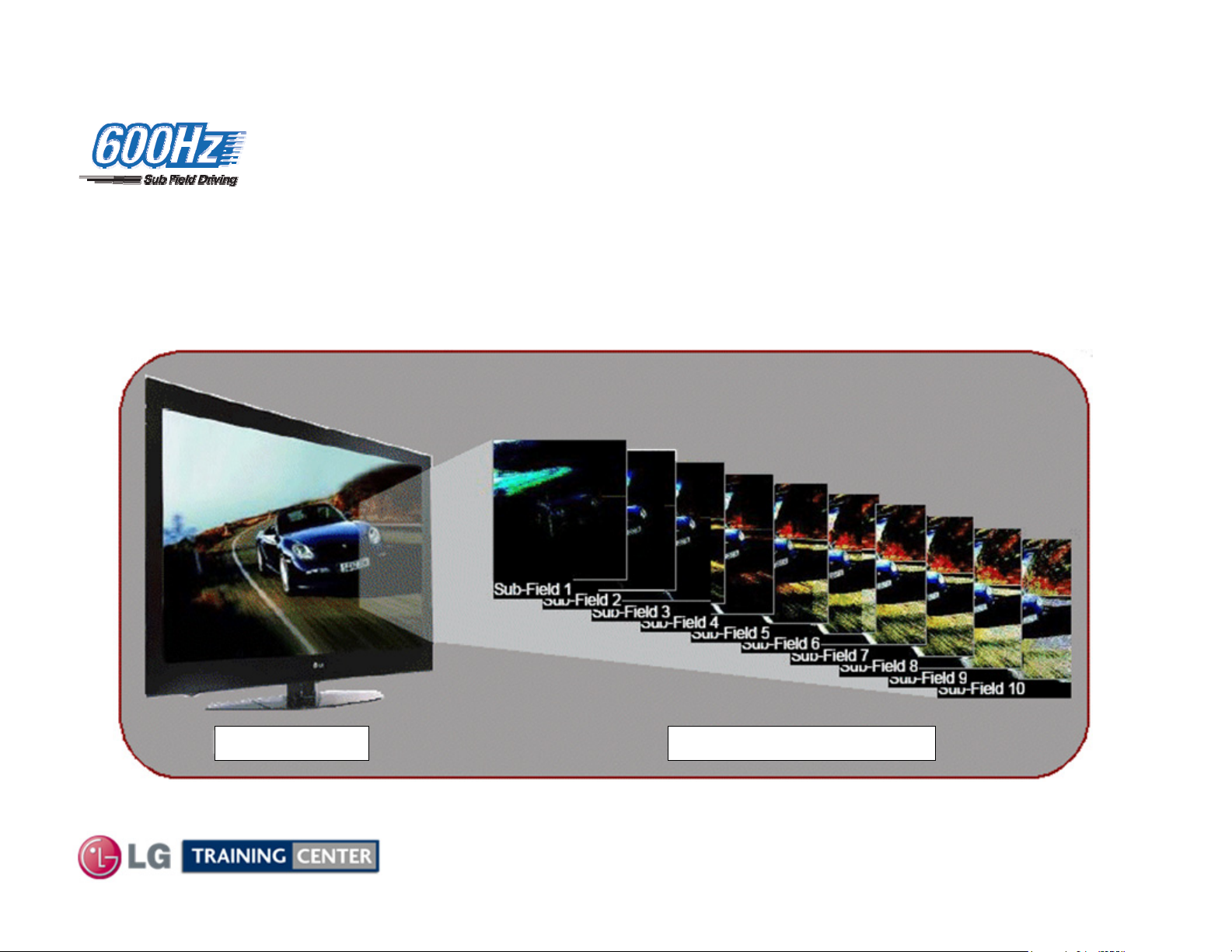
600Hz Sub Field Driving
600Hz Sub Field Driving
(600 Hz Sub Field Driving)
• 600 Hz Sub Field Driving is achieved by using 10 sub-fields per frame process
(vs. Comp. 8 sub-field/frame)
• No smeared images during fast motion scenes
Original Image 10 Sub Fields Per Frame
Sub Field firing occurs using wall charge and polarity differences between Y-SUS and Z-SUS signals.
14
July 2010 50PJ350 Plasma
Page 15
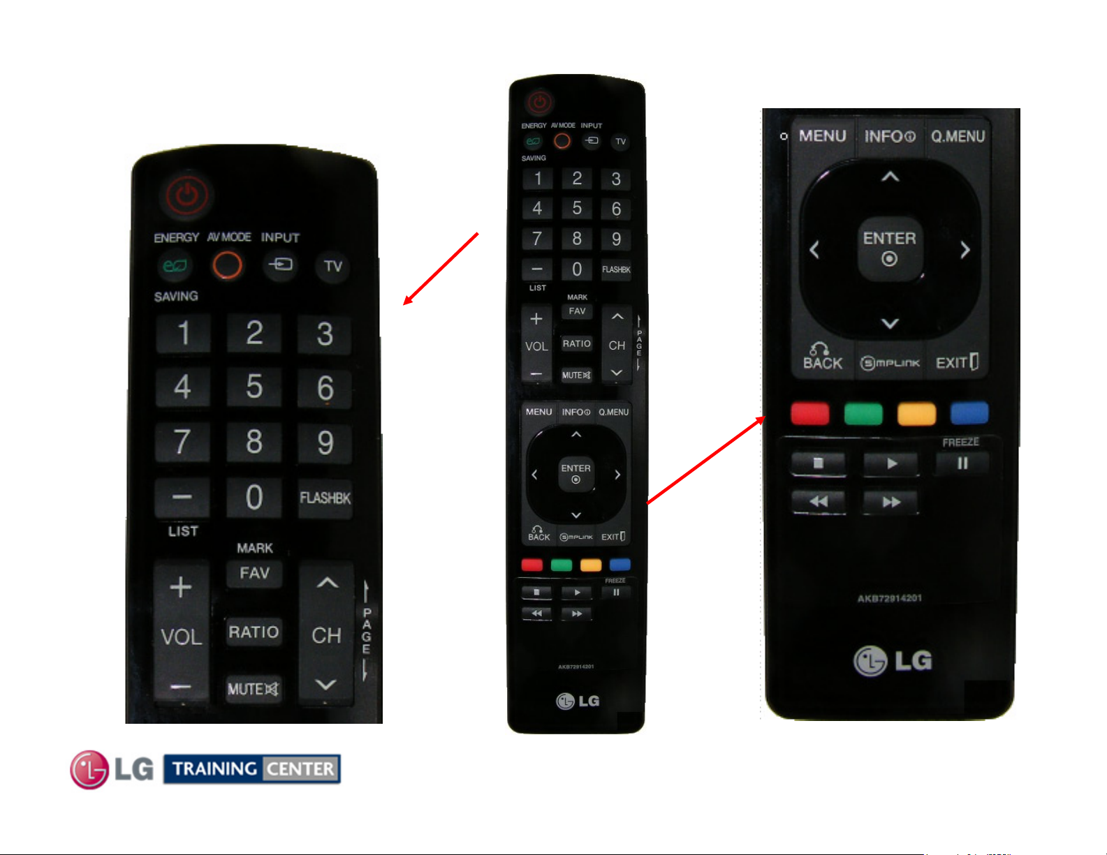
50PJ350 Remote Control
50PJ350 Remote Control
p/n AKB72914201
TOP PORTION
BOTTOM PORTION
15
July 2010 50PJ350 Plasma
Page 16

50PJ350 Rear and Side Input Jacks
50PJ350 Rear and Side Input Jacks
REAR
INPUTS
AC In
USB for Music, Photos
and Software
Upgrades
SIDE
INPUTS
USB
HDMI 3
Composite
Video/Audio
16
July 2010 50PJ350 Plasma
Page 17
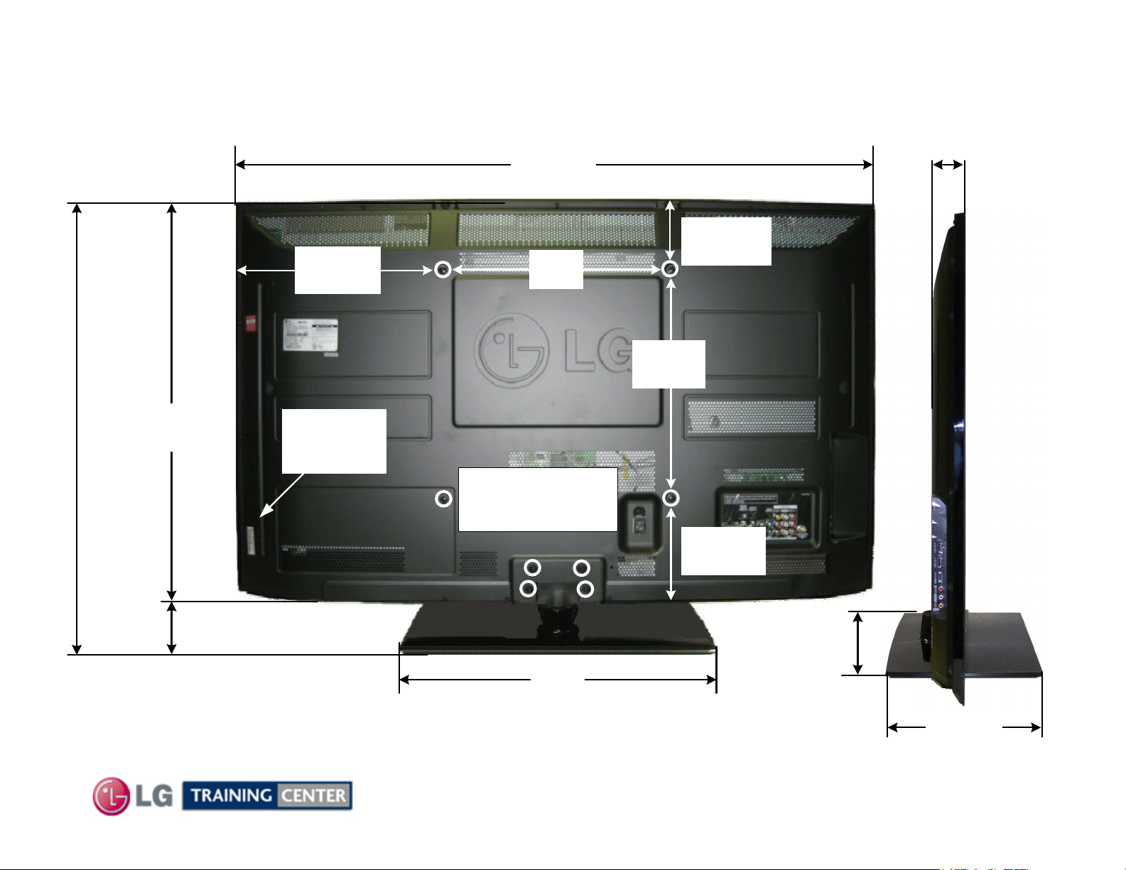
50PJ350 Dimensions
Power:
340W (Typical)
0.1W (Stand-By)
30-13/16"
782.32mm
28-3/8"
721.36mm
There must be at least 4 inches of Clearance on all sides
15-3/16”
385.8mm
Model No.
Serial No.
Label
46-1/8"
1170.94mm
15-3/4"
400mm
Remove 4 screws
to remove stand
for wall mount
2-3/16"
55.88mm
5-1/4”
133.6mm
15-3/4"
400mm
7-3/8”
187.2mm
2-3/8"
60.96mm
Weight:
78.5 lbs with Stand
60.8 lbs without Stand
2-3/4"
70mm
20-7/8"
530mm
12-3/16"
309.88mm
17 July 2010 50PJ350 Plasma
Page 18
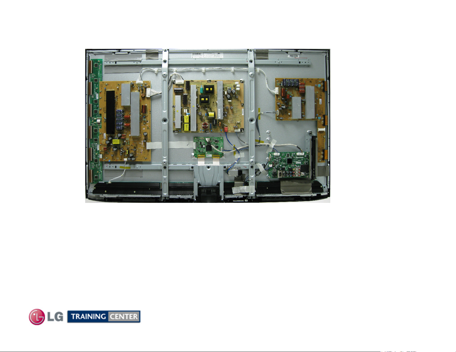
DISASSEMBLY SECTION
DISASSEMBLY SECTION
This section of the manual will discuss Disassembly, Layout and Circuit
Board Identification, of the 50PJ350 Advanced Single Scan Plasma Display Panel.
Upon completion of this section the Technician will have a better
understanding of the disassembly procedures, the layout of the printed
circuit boards and be able to identify each board.
18
July 2010 50PJ350 Plasma
Page 19
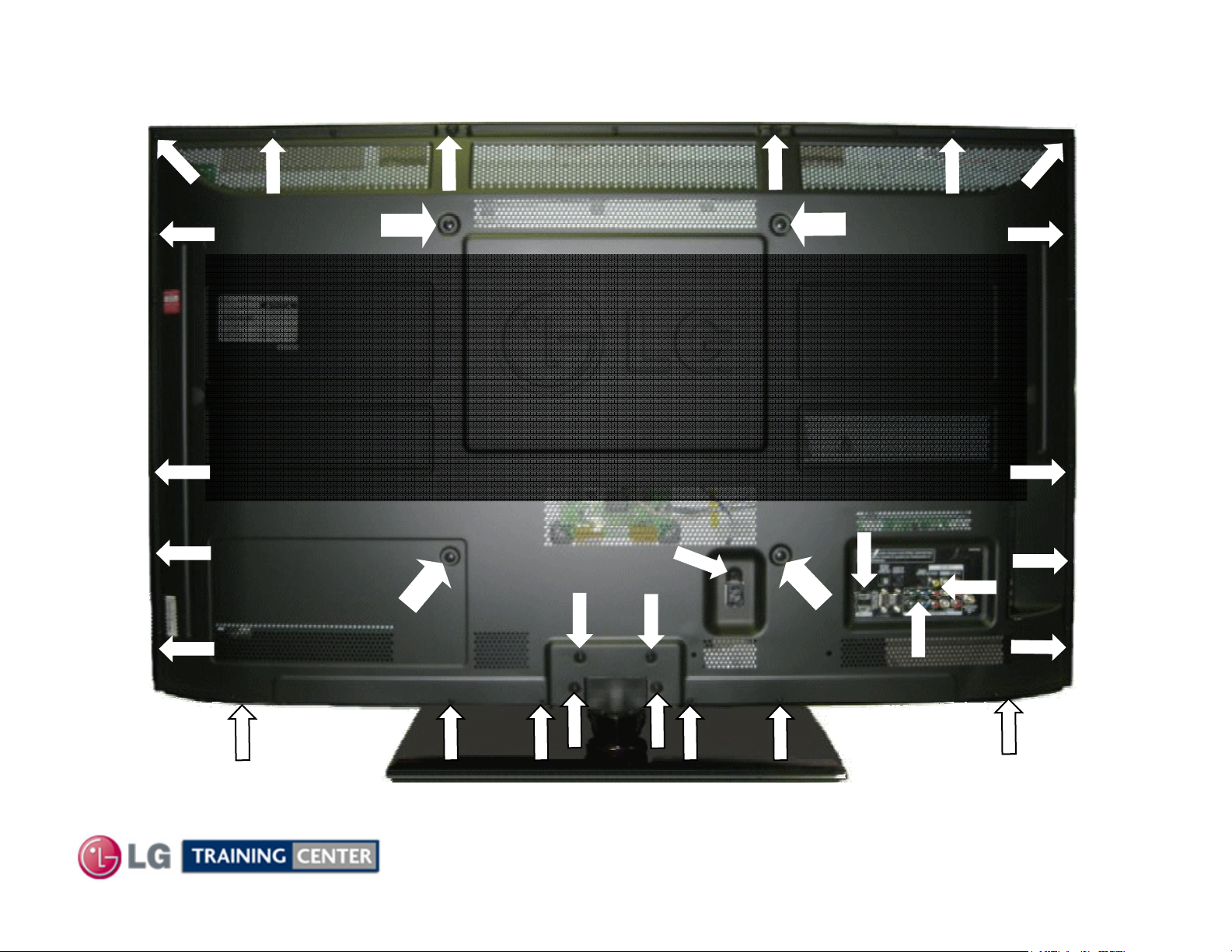
Removing the Back Cover
Removing the Back Cover
To remove the back cover, remove the 32 screws
(The Stand does not need to be removed).
PAY CLOSE ATTENTION TO THE TYPE, SIZE AND LENGTH
Of the screws when replacing the back cover.
Improper type can damage the front.
Indicated by the arrows.
19
July 2010 50PJ350 Plasma
Page 20
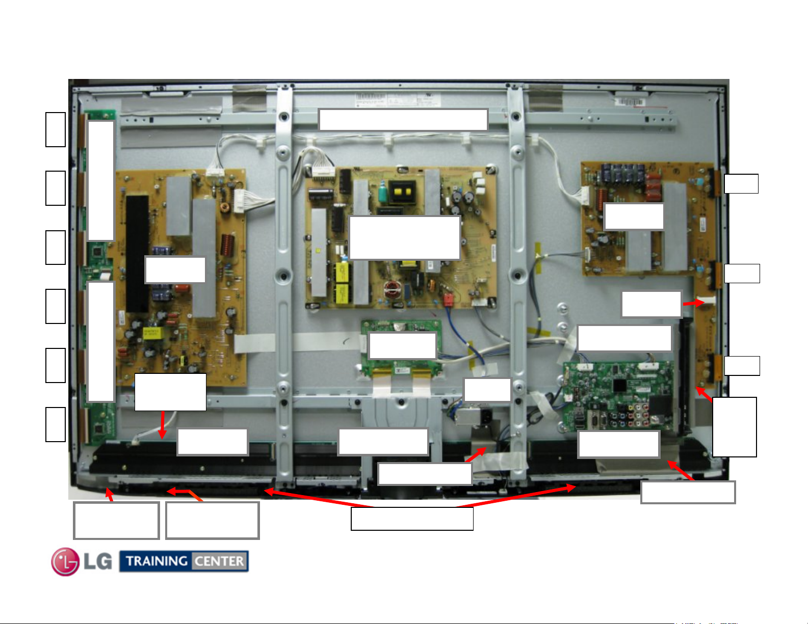
Circuit Board Layout
Circuit Board Layout
Identifying the Circuit Boards
Identifying the Circuit Boards
FPC
FPC FPC
FPC
FPC FPC
Y-Drive Upper
Y-SUS
Y-Drive Lower
TCP
Heat Sink
Left “X”
Panel Voltage and Panel ID Label
Power Supply
(SMPS)
Control
Center “X”
AC In
Z-SUS
Z-SUB
Main Board
Right “X”
FPC
FPC
FPC
Side
Input
(part of
main)
IR/LED
Board
Soft Touch
Keyboard
Conductive Tape
Invisible Speakers
20
Conductive Tape
July 2010 50PJ350 Plasma
Page 21
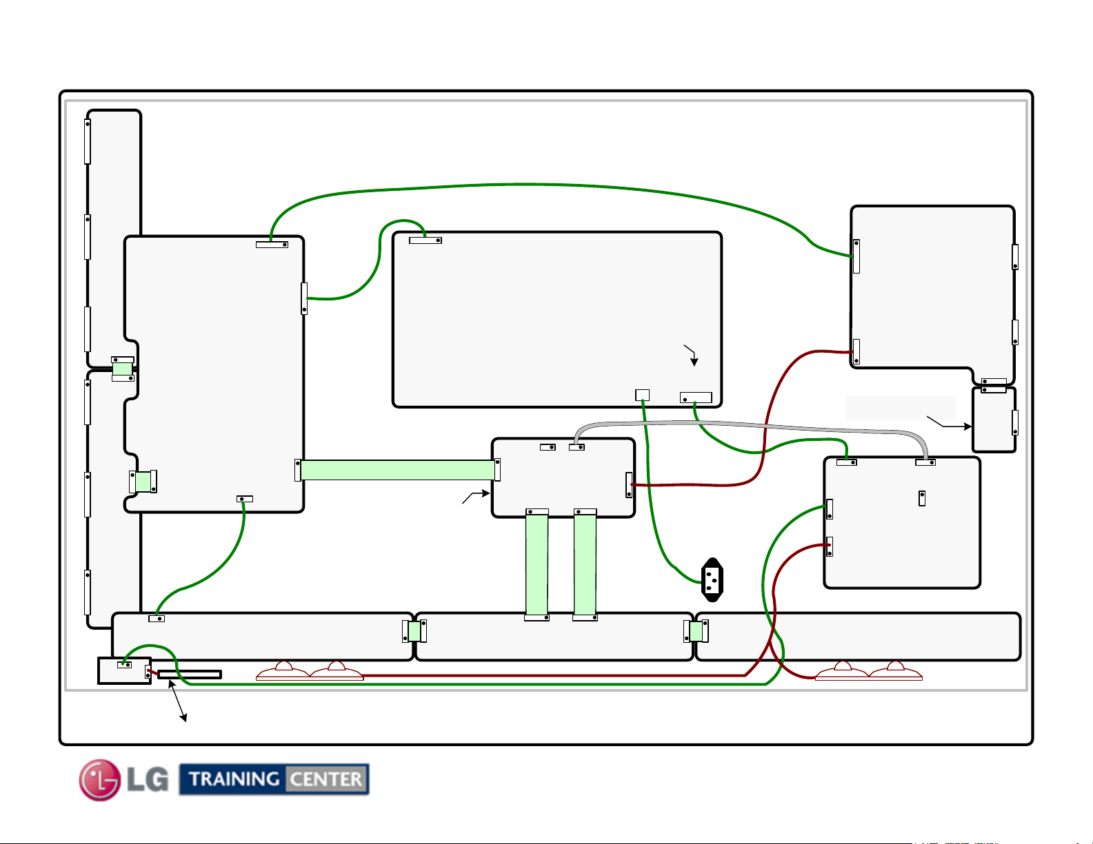
50PJ350 Connector Identification Diagram
50PJ350 Connector Identification Diagram
PANEL
p/n: EAJ60716304 (PDP50T10000.ADLGB)
P101P102P103
Y-DRIVE
p/n: EAJ60716316 (PDP50T10000.ASLGB)
UPPER
p/n: EBR63551601
Board
P211
P812
P2
Z-SUS
Board
P101
P201P202P203
P100
P110
P204
p/n: EBR63551701
P101
p/n: EBR63039801
P212P205
Y-DRIVE
LOWER
Board
P122
LEFT X
Y-SUS
Board
P203
Board
P210
P101
p/n: EBR64062301
P111
p/n: EBR63549501
P121 P212
p/n: EBR64062201
SMPS
POWER SUPPLY
Board
p/n: EAY60968701
P102
n/c
P121
CONTROL
Board
P161
P231
P101
P162
P210
CENTER X
Top row Odd
Back row Even
SC101
LN
P813
P211
AC
In
P331
LVDS
p/n: EBR63040301
P1
Z-SUB Board
P301
P704
P801
p/n: EBT60953802
RIGHT X
Board
P102
P3
P202
P703
P900
n/c
MAIN
Board
p/n: EBR64062001
P7
FRONT IR
p/n: EBR65007704
Speakers (Front Right)
Front “Soft Switch” Key Pad
21
p/n: EAB60962801p/n: EAB60962801
Speakers (Front Left)
July 2010 50P
J350 Plasma
Page 22
Disassembly Procedure for Circuit Board Removal
Disassembly Procedure for Circuit Board Removal
Note: 1) Remember to be cautious of ESD as some semiconductors are CMOS and prone to static failure.
Switch Mode Power Supply Board Removal
Disconnect the following connectors: P812, P813 and SC101.
Remove the 9 screws holding the SMPS in place.
Remove the board.
When replacing, be sure to readjust the Va/Vs voltages in accordance with the Panel Label.
Also, re-confirm VSC, -Vy and Z-Bias as well.
Note: The Y-SUS does not come with the
Y-SUS Board Removal
Disconnect the following connectors: P210, P211, P212 and Ribbon Cable P110.
To remove P110, lift up on the locking mechanism and pull the ribbon cable out.
Remove the 16 screws holding the Y-SUS in place. Do not run the set with P117 or P118 removed.
Remove the Y-SUS board. When replacing, be sure to readjust the Va/Vs voltages in accordance with the
Panel Label.
Confirm VSC, -Vy and Z-bias as well.
Y-Drive Boards Removal
Note: The Y-SUS does not come with the
connectors between the Y-SUS and Y-Drive
connector to the Lower Y-Drive
Board Standoff
Disconnect the following Flexible Ribbon Connectors P101~P103 and/or P201~P203:
Disconnect P212 by pulling the ribbon cable upward. Remove P204 or P110 by lifting up
on the locking mechanism and pull the ribbon cable out. Do not run the set with these
connectors removed. Remove the 3 screws holding either of the Y-Drive boards in place.
Lift up slightly, the slide to the left. Remove the Y-Drive Board.
Note: Y-SUS, Z-SUS and Y-Drive boards are mounted on board stand-offs that have a small collar.
The board must be lifted slightly to clear these collars. Behind each board are “Chocolate” (dense rubber
like material) that act as shock absorbers. They may make the board stick when removing.
22
July 2010 50PJ350 Plasma
Collar
Page 23
Disassembly Procedure for Circuit Board Removal (2)
Disassembly Procedure for Circuit Board Removal (2)
Z-SUS Board Removal
Disconnect the following connectors: P1 and P2, then P101, P102 and P202 by pulling out the locking
mechanism and pulling out the FPC to the panel.
Remove the 11 screws holding the board in place.
Remove the two screws in the Z-SUB board. Lift up slightly to clear the screw stand-offs and pull the
Z-SUS to the left. Unseat P3/P7 from the Z-SUB board and remove the board.
When replacing, be sure to readjust the Va/Vs voltages in accordance with the Panel Label.
Confirm VS, -Vy and Z-bias as well.
Z-SUB Board Removal
Remove the two screws in the Z-SUB board. Remove P202 by pulling out the locking mechanism and
pulling out the FPC to the panel. Remove the board.
Main Board Removal
Disconnect the following connectors: P703 LVDS and P301 (press gently inward on the locking tabs)
and pull out, P704 and P801. Remove 1 screw in the decorative plastic piece and remove.
Remove the 4 screws holding the Main board in place and Remove the board.
Control Board Removal
Disconnect the following connectors: P12 LVDS, P111 Ribbon and P101, P102, P104 Ribbons by lifting
up the locking tab. Remove the 2 screws holding the Control board in place. Lift up the Control board to
unseat it from the two metal supports at the bottom and Remove the board.
Front IR and Key Pad Removal
FRONT IR/INTELLIGENT SENSOR and POWER BUTTON:
Disconnect P100 and P101. Note: P101 is a ribbon connector. Lift up the locking mechanism and
slide the ribbon cable out. Remove the Board by lifting up on the top tabs, lift the board and remove.
KEY PAD:
The Key Pad is a thin strip of static sensitive material attached to the front glass. It is not removable.
23
July 2010 50PJ350 Plasma
Page 24

X Drive Circuit Board Removal Continued
X Drive Circuit Board Removal Continued
Make sure AC is removed.
Lay the Television down carefully on a padded surface.
Make sure to use at least two people for this process so as not to flex the panel glass.
a) Remove the Back Cover.
b) Remove the Stand (4 Stand Screws were removed during back removal).
c) Remove the Stand Metal Support Bracket (5 Screws) 2 Plastic tap thread and 3 Metal thread.
d) Remove the two Vertical support Braces marked “E”.
Note: There are
(Note, the right brace has a Grounding wire from the AC input which must also be removed).
e) Remove the 10 screws holding the Heat Sink. (Warning: Never run the set with this heat sink
removed).
To remove the heat sink, lift up to release the tacky Chocolate (heat transfer material) and slide the
heat sink to the left to clear the connector wires on the right side.
Note: There are two large pieces of conductive tape on the right side of the Right X Board that must
be removed.
Also, note that there several pieces of Chocolate heat transfer material attached all the way across the
underside of the heat sink.
5 Screws per/brace, 2 Plastic tap thread and 3 Metal thread.
X-DRIVE LEFT, CENTER AND RIGHT REMOVAL:
Disconnect all TCP ribbon cables from the defective X-Drive board and all other Ribbon cables going to
the board.
Remove the (3 Left or Right X) or (5 Center X) screws holding the defective X-Drive board in place.
Remove the board. Reassemble in reverse order. Recheck Va / Vs / VScan / -VY / Z-Drive.
24
July 2010 50PJ350 Plasma
Page 25

Getting to the X Circuit Boards
Getting to the X Circuit Boards
With Stand removed
D
Left
Warning:
Never run the TV with the
TCP Heat Sink removed
E
Heat Sink
D
Right
C
Ground
Wire
C
B
Warning Shorting Hazard: Conductive Tape. Do not allow to touch energized circuits.
25
July 2010 50PJ350 Plasma
Page 26
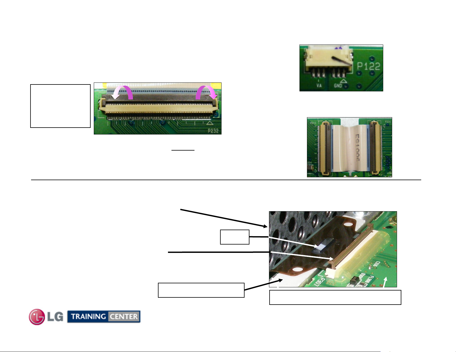
Left and Right X Drive Connector Removal
Left and Right X Drive Connector Removal
Disconnect connector P122
See below to Remove the Connections on the X-Boards.
From the Control Board to the X-Boards.
There may be tape on these connectors.
P231, P232
P121, P212
P211, P331
Are the same
Remove tape (if present) and Gently
locking mechanism upward and remove the ribbon
cable from the connector.
Removing Connectors to the TCPs.
pry the
Va from the
Y-SUS to
Left X Only
Connectors from Center to Left and
Center to Right X Boards
P121 to P212
Left to Center X
P211 to P331
Center to Right X
Carefully lift the TCP ribbon up and off.
It may stick, be careful not to crack TCP.
(See next page for precautions)
Gently lift the locking mechanism
upward on all TCP connectors
Left X: P101~108
Center X: P201~207
Right X: P301~308
Cushion (Chocolate)
TCP
26
Example
Flexible ribbon cable connector
July 2010 50PJ350 Plasma
Page 27
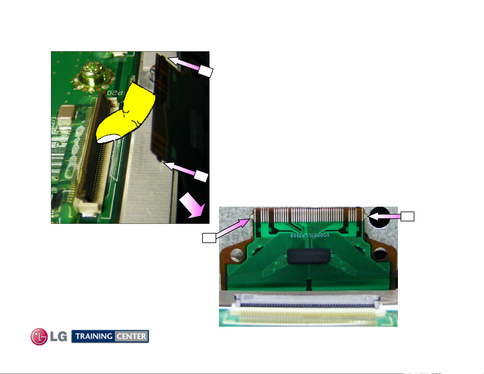
TCP (Tape
TCP (Tape
Carrier
Carrier
Package) Generic Removal Precautions
Package) Generic Removal Precautions
T
a
b
Lift up the lock as shown using your fingernail.
(The Lock can be easily broken.
It needs to be handled carefully.)
T
a
b
Separate the TCP from the connector as shown.
TCP Film can be easily damaged.
Handle with care.
The TCP has two small tabs on each
side which lock the ribbon cable
fully into the connector. They have
to be lifted up slightly to pull the
connector out.
Note: TCP is usually stuck down
to the Chocolate heat transfer
material, be Very Careful when
lifting up on the TCP ribbon cable.
Tab
27
Tab
July 2010 50PJ350 Plasma
Page 28
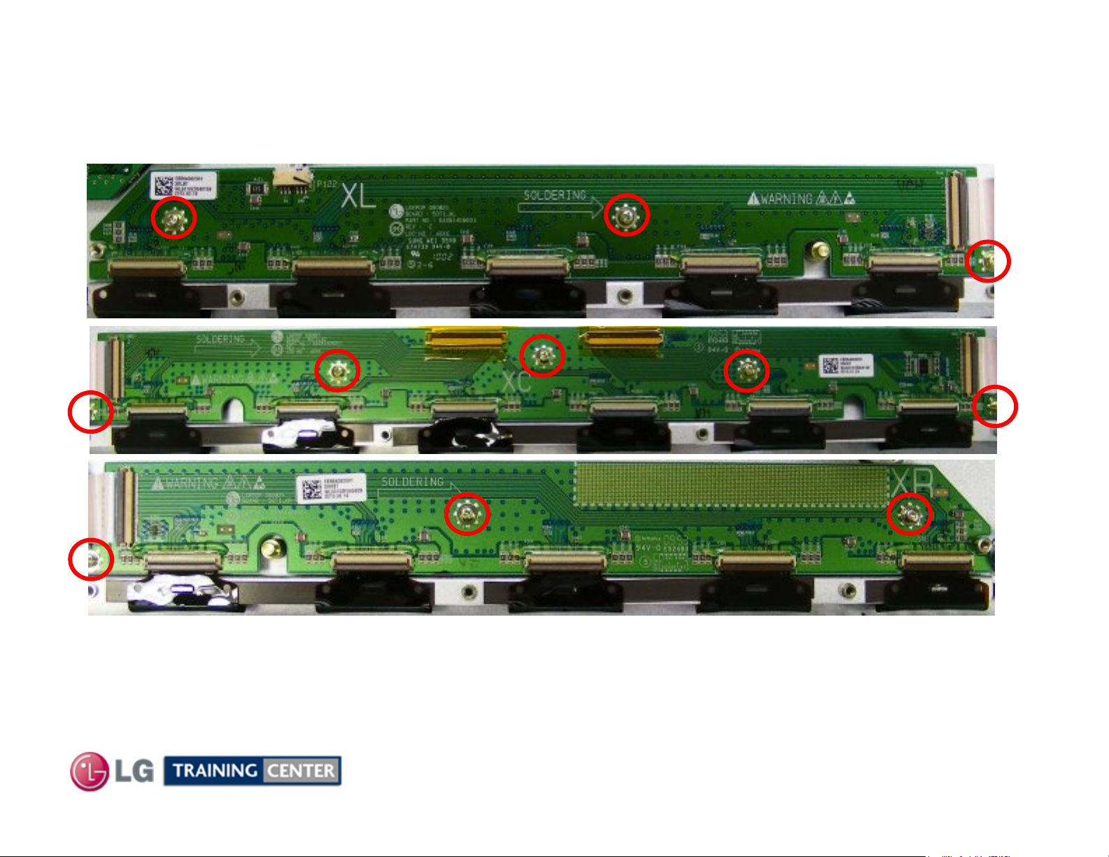
Left, Center and Right X Drive Removal
Left, Center and Right X Drive Removal
Remove the 3 screws in Left or Right X-Boards or 5 in the Center X-Board. (9 Total)
(Some screws are shared between boards)
The Left X Board drives the Right 5/16 of the side of the screen vertical electrodes
The Center X Board drives the Center 3/8 of the of the screen vertical electrodes
The Right X Board drives the Left 5/16 of the side of the screen vertical electrodes
28
July 2010 50PJ350 Plasma
Page 29
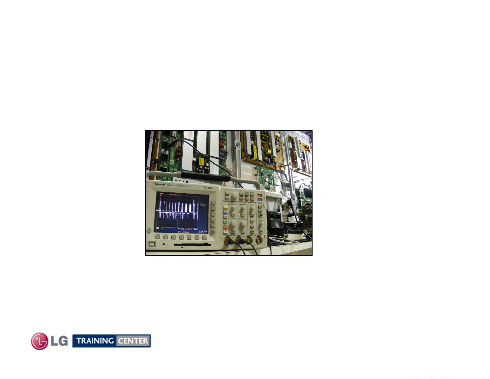
CIRCUIT OPERATION, TROUBLESHOOTING AND CIRCUIT ALIGNMENT SECTION
CIRCUIT OPERATION, TROUBLESHOOTING AND CIRCUIT ALIGNMENT SECTION
50PJ350 Plasma Display
This Section will cover Circuit Operation, Troubleshooting and Alignment of the
Power Supply, Y-SUS Board, Y-Drive Boards, Z-SUS Board, Control Board,
Main Board and the X Drive Boards.
At the end of this Section the technician should understand the operation of each
circuit board and how to adjust the controls. The technician should be able with
confidence to troubleshoot a circuit board failure, replace the defective circuit and
perform all necessary adjustments.
29
July 2010 50PJ350 Plasma
Page 30
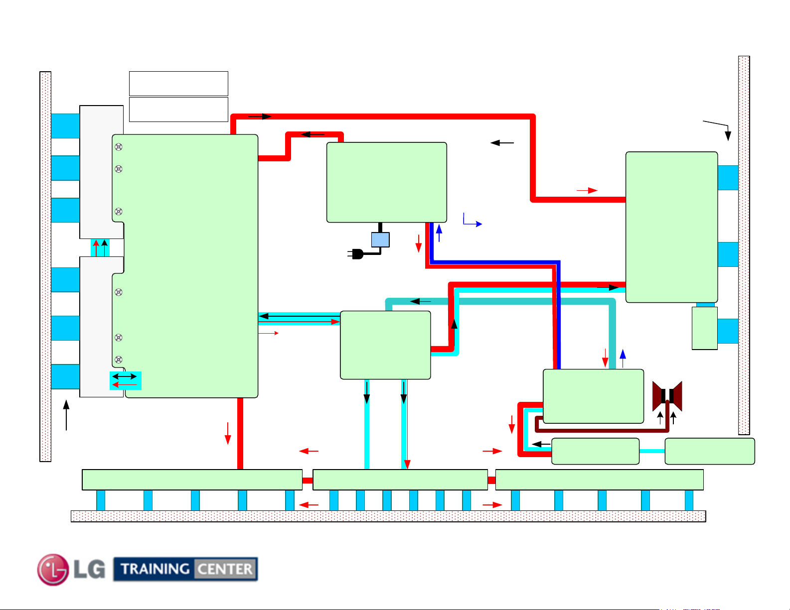
50PJ350 Signal and Voltage Distribution Block
Y Drive
Upper
FPCs
P101
P102
5VFG (5V) measured
from Floating Ground
15VFG (15V) measured
from Floating Ground
FG
FG
Y-SUS Board
P103
FPCs
P201
P202
P203
P110
P204
P205
Y Drive
Scan
P110 / P204
Floating Gnd (FG)
Drive Signals, FG5V
and Vscan.
FG5V
Scan
FG15V
16V
VSC
-VY
FG
FG
P212
Floating Gnd (FG)
Drive Signals, FG5V
Lower
Display Panel Horizontal
Electrodes Reset, Sustain
P211
P210
P101
P114
Va
P122
SMPS TURN ON SEQUENCE
Step 1: RL_ON: 17V, 5V, AC_Det, Error Det,
Step 2: M_On: M5V, Va, Vs
P812
M5V, Vs, Va
Note:
Va not used
by Y-SUS only
fused and routed
to the X-Board
Logic Signals
SMPS
Board
SK101
AC
Input
Filter
LVDS
Display Enable
Video
To Y-SUS and Y-Drive
P121
Board
P161
P162
16V / M5V
Note: 16V not used
by Control
P111
CONTROL
RGB Logic
Signals
3.3V
P121 P212
P231
P232
P232
P211 P311 P331
X-Board-Center
Va
P813
P101
3.3V
RGB Logic
Signals
3.3V
SMPS OUTPUT VOLTAGES IN STBY
STB +5V
SMPS OUTPUT VOLTAGES IN RUN
STB5V, +5V, 17V to Main Board
Vs, Va and M5V to Y-SUS,
Error Com
SMPS
Turn On
Vs
Commands
RL_ON
M_On
17V, +5V, AC Det
M5V, Va, Vs
16V / M5V
Stand By:
STB +5
Run:
AC Det +5, 17V
P301
P703
MAIN Board
P704
3.3V
STBY
3.3V
P211 P331
Va
P801
Intelligent Sensor
P100
X-Board-RightX-Board-Left
IR,
Display Panel
Horizontal
Electrodes
Sustain
Z-SUS
Board
P2
Z Drive Control
P1
Signals
Z-SUB
Board
Speakers
Soft Touch Keys
And Power Button
P101
FPCs
P101
P102
P3
P7
P202
FPCs
3.3V
Key Board
Pull Up
P101 P102 P103 P104 P201 P203 P204 P206 P301 P302 P303 P305
P105 P202 P205 P304
Display Panel Vertical Address (Colored Cell Address)
30
July 2010 50PJ350 Plasma
Page 31
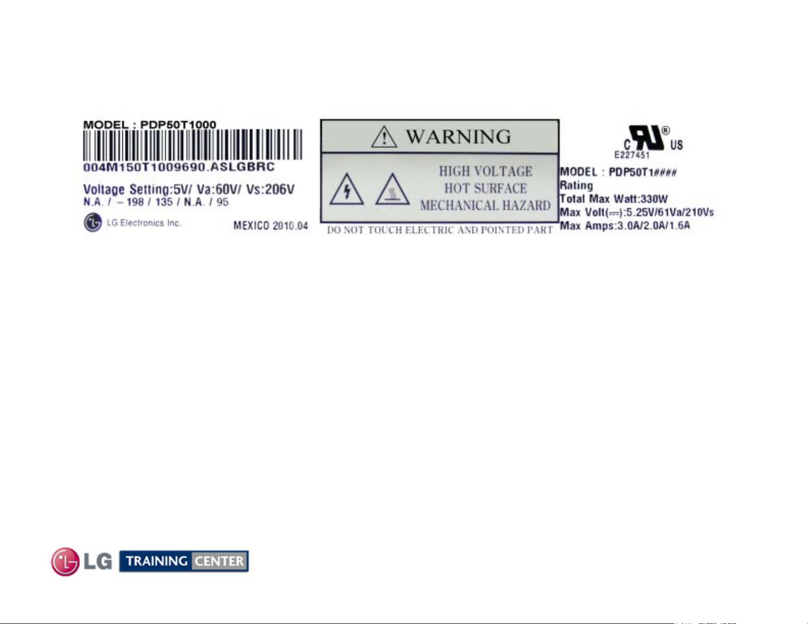
Panel Label Explanation
Panel Label Explanation
(1)
(8)
(2)
(3)
(4)
(5)
(6) (7)
(1) Panel Model Name
(2) Bar Code
(3) Manufacture No.
(4) Adjusting Voltage DC, Va, Vs
(5) Adjusting Voltage (Set Up / -Vy / Vsc / Ve / Vzb)
(6) Trade name of LG Electronics
(9)
(10)
(11)
(9) TUV Approval Mark (Not Used)
(10) UL Approval Mark
(11) UL Approval No.
(12) Panel Model Name
(13) Max. Watt (Full White)
(14) Max. Volts
(12)
(13)
(14)
(15)
(7) Manufactured date (Year & Month)
(8) Warning
31
(15) Max. Amps
July 2010 50PJ350 Plasma
Page 32
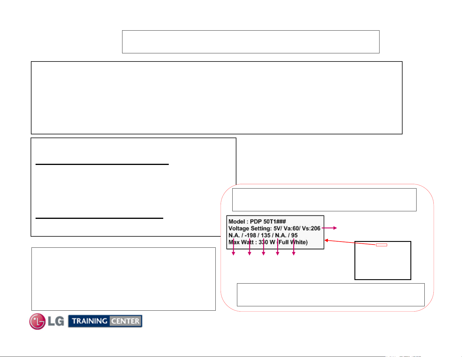
Adjustment Notice
Adjustment Notice
All adjustments (DC or Waveform) are adjusted in WHITE WASH.
Customer’s Menu, Select “Options”, select “ISM” select “WHITE WASH”.
It is critical that the DC Voltage adjustments be checked when;
1) SMPS, Y-SUS or Z-SUS board is replaced.
2) Panel is replaced, Check Va/Vs since the SMPS does not come with new panel
3) A Picture issue is encountered
4) As a general rule of thumb when ever the back is removed
ADJUSTMENT ORDER “IMPORTANT”
DC VOLTAGE ADJUSTMENTS
1) POWER SUPPLY: VS, VA (Always do first)
2) Y-SUS: Adjust –Vy, VSC
Remember, the Voltage Label MUST be followed,
3) Z-SUS: Adjust Z-Bias (VZB)
it is specific to the panel’s needs.
WAVEFORM ADJUSTMENTS
1) Y-SUS: Set-Up, Set-Down
The Waveform adjustment is only necessary
1) When the Y-SUS board is replaced
2) When a “Mal-Discharge” problem is
encountered
3) When an abnormal picture issues is
encountered
Set-UpVe-Vy Vsc
All label references are from a specific panel.
They are not the same for every panel encountered.
32
Power Supply
ZBias
Panel
“Rear View”
July 2010 50PJ350 Plasma
Page 33
SWITCH MODE POWER SUPPLY SECTION
SWITCH MODE POWER SUPPLY SECTION
This Section of the Presentation will cover troubleshooting the Switch Mode Power Supply for
the Single Scan Plasma. Upon completion of the section the technician will have a
better understanding of the operation of the Power Supply Circuit and will be able to
locate voltage and test points needed for troubleshooting and alignments.
• DC Voltages developed on the SMPS
• Adjustments VA and VS.
Always refer to the Voltage Sticker located on the back of the panel, in the upper Left Hand
side for the correct voltage levels for the VA, VS, -VY, VSC, and Z Bias as these voltages
will vary from Panel to Panel even in the same size category.
Set-Up and Ve are just for Label location identification and are not adjusted in this panel.
SMPS p/n: EAY60968701
Check the silk screen label on the top center of the Power Supply board to identify the correct part
number. (It may vary in your specific model number).
On the following pages, we will examine the Operation of this Power Supply.
33
July 2010 50PJ350 Plasma
Page 34
Switch Mode Power Supply Overview
Switch Mode Power Supply Overview
The Switch Mode Power Supply Board Outputs to the :
Y-SUS Board
Z-SUS Board
Main Board
Adjustments
VS
VA
M5V
VS
STBY 5V Microprocessor Circuits
17V Audio B+ Supply, Tuner B+ Circuits
5V Signal Processing Circuits
Also AC_Det (if missing, shuts of TV in 10 seconds) and Error_Det (not used)
There are 2 adjustments located on the Power Supply Board VA and VS. The
M5V is pre-adjusted and fixed. All adjustments are made referenced to Chassis
Ground. Use “Full White Raster” 100 IRE
Drives the Display Panel’s Horizontal Electrodes.
To Y-SUS, fused then to the X-Boards. (Not used by Z-SUS).
Primarily responsible for Display Panel Vertical Electrodes.
Used to develop Bias Voltages on the Y-SUS then routed to the Control
board and then to the Z-SUS Board.
VS is routed to the Y-SUS first then to the Z-SUS board which
Drives the Display Panel’s Horizontal Electrodes.
VS
VA
VR901
VR502
34
July 2010 50PJ350 Plasma
Page 35
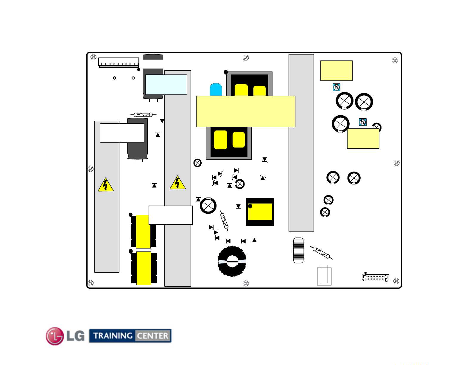
Power Supply Board Layout (Drawing)
Power Supply Board Layout (Drawing)
VA TP
VS TP
F801
4A
250V
Stand-By: 0.9V
Run: 388V
P812
VS and VA
D805
D601
Stand-By: 1.5V
L601
TP
ZD803
Run: 388V
SMPS
p/n: EAY60968701
ZD302
D307
ZD303
D601
D308
D309
D306
D302
D609
ZD301
D303
D305
F302
2.5A
250V
T901
T301
D103
D301
T902
ZD401
ZD101
VR901
VS Adj
VR502
VA Adj
F101
10A
250V
L602
35
P813
SC101
July 2010 50PJ350 Plasma
Page 36
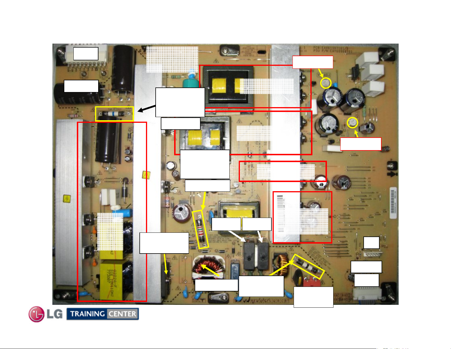
Power Supply Circuit Layout
Power Supply Circuit Layout
P812
To Y-SUS
Primary
Source
Fuse F801
0.9V Stby
388V Run
4Amp/250V
2.5Amp/250V
Fuse F302
1.5V Stby
388V Run
VS Source
VA Source
17V Source
STBY 5V,
RL103RL104
5V Source
VS VR901
VA VR502
PFC
Circuit
Bridge
Rectifier
10Amp/250V
36
Main Fuse
F101
July 2010 50PJ350 Plasma
N/C
To MAIN
P813
AC Input
SC 101
Page 37

Power Supply Basic Operation
Power Supply Basic Operation
AC Voltage is supplied to the SMPS Board at Connector SC101 from the AC Input assembly, routed to the Standby 5V
supply. The STBY5V (standby) is B+ for the Controller chip on the back of the board (IC701) on the SMPS and output at
P813 pins 13 and 14 then sent to the Main board for Microprocessor (IC1) operation (STBY 3.46V RUN 5.14V).
When the Microprocessor (IC1) on the Main Board receives a “POWER ON“ Command from either the Power button or
the Remote IR Signal, it outputs a high (2.43V) called RL_ON at Pin 15 of P813. This command causes the Relay Circuit to
close both Relays RL101 and RL103 routing AC to the Bridge Rectifier D101 which then routes the primary voltage to the
PFC circuit (Power Factor Controller) 388V which can be read measuring voltage at Fuses F302 and F801 from “Hot”
Ground. AC Detection (AC Det) is generated on the SMPS, by rectifying a small sample of the A/C Line and routed to the
Controller (IC701) where it outputs at P813 pin 16 (4.44V) and sent to P301 to the Main Board where it is sensed and
monitored by the Main Microprocessor (IC1). If AC Det is missing the set will come on, but shut off in 10 seconds.
When RL_ON arrives, the run voltage +5V source becomes active and is sent to the Main Board via P813 (5.17V at
pin 5, 6 and 7). The (Error Det) from the SMPS Board to the Main Board can be measured at pin 8 of P813 (2.85V STBY
and 4.90V RUN), but it is not used. The RL-ON command also turns on the 17V (Audio B+) which is also sent to the Main
Board. The 17V Audio supply outputs to the Main board at P813 pins 1 and 2 and used for Audio processing and
amplification.
The next step is for the Microprocessor IC1 on the Main Board to output a high (3.29V) on M_ON Line to the SMPS at P813
Pin 17 which is sensed by the Controller IC701, turning on the M5V line and outputs at P812 pins 9 and 10 to the Y-SUS
board.
The Controller (IC701) also uses the M_ON line to turn on the VA and the VS supplies. (Note there is no VS On Command
in this set). VS is output at P812 to the Y-SUS board P210. (VA pins 6 and 7 and VS pins 1 and 2). Note: The Va is fused
on the Y-SUS then routed out P203 to the X-Board Left. VS is also routed out of the Y-SUS P211 pins 4 and 5 to the Z-SUS
P2.
AUTO GND Pin 18 of P813: This pin is grounded on the Main board. When it is grounded, the Controller (IC701) works in
the normal mode, meaning it turns on the power supply via commands sent from the Main board. When AUTO GND is
floated (opened), it pulls up and places the Controller (IC701) into the Auto mode. In this state, the Controller turns on the
power supply in stages automatically. A load is necessary to perform a good test of the SMPS if the Main board is suspect.
37
July 2010 50PJ350 Plasma
Page 38
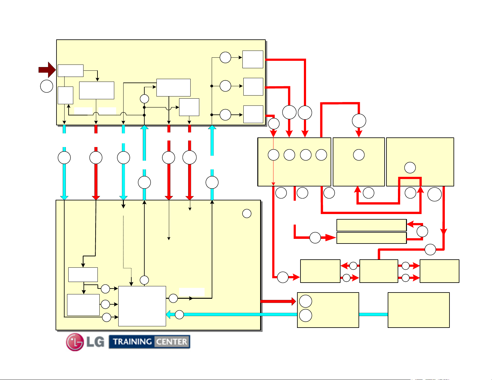
50PJ350 POWER SUPPLY START UP SEQUENCE
50PJ350 POWER SUPPLY START UP SEQUENCE
In Stand-By Primary side is 1.5V
F302
In Run (Relay On) Primary side is 388V
F801
AC In
1
AC
Det
By 5V Reg
STBY RUN
3.46V 5.14V
Stand-By 0.9V
Run 388V
Stand
POWER SUPPLY
(SMPS)
+5V
Regulator
5
17V
Reg
Vs
Va
M5V
Vs
Va
8
9
7
Vs
9
7
9
8
M5V
Reg
Reg
Reg
AC
Det.
If
missing
set
shuts
off in 10
Sec.
AC Det.
If missing,
set will not
turn on.
3.3V Reg
IC302
Reset
C108, D1,
Stand By
R62
5V
26
3.3VST
2
3
6
Error Det.
6
Not
Used
Error Det.
Error
Det.
Microprocessor
RL On
5
5
Relay
On
IC1
5V
6
+5V HDMI
EDID
And other
circuits
7
4
17V
6
17V
Audio
IC801
M_On
M_On
7
At point
TV is in
Stand-By
state. It is
Energy Star
Compliant.
Less than 1
Watt
3
MAIN
Board
Power On
Vs
M5V
8
9
Y-SUS Z-SUS
Va
5VFG
8
5V
Floating
Gnd
16V
7 778
16V / M5V
8
X PWB
8
3.3V_ST
Left
2
4
Front IR
Board
VsVsVa
99 7
CONTROL
7
16V / M5V
Y DRIVE Upper
Y DRIVE Lower
3.3V 3.3V
3.3V
7 7
X PWB
8
Center
8
Va Va
Touch
Key Pad
M5V
3.3V
7
8
7
X PWB
Right
Soft
38
Remote Power Key
July 2010 50PJ350 Plasma
Power Key
Page 39
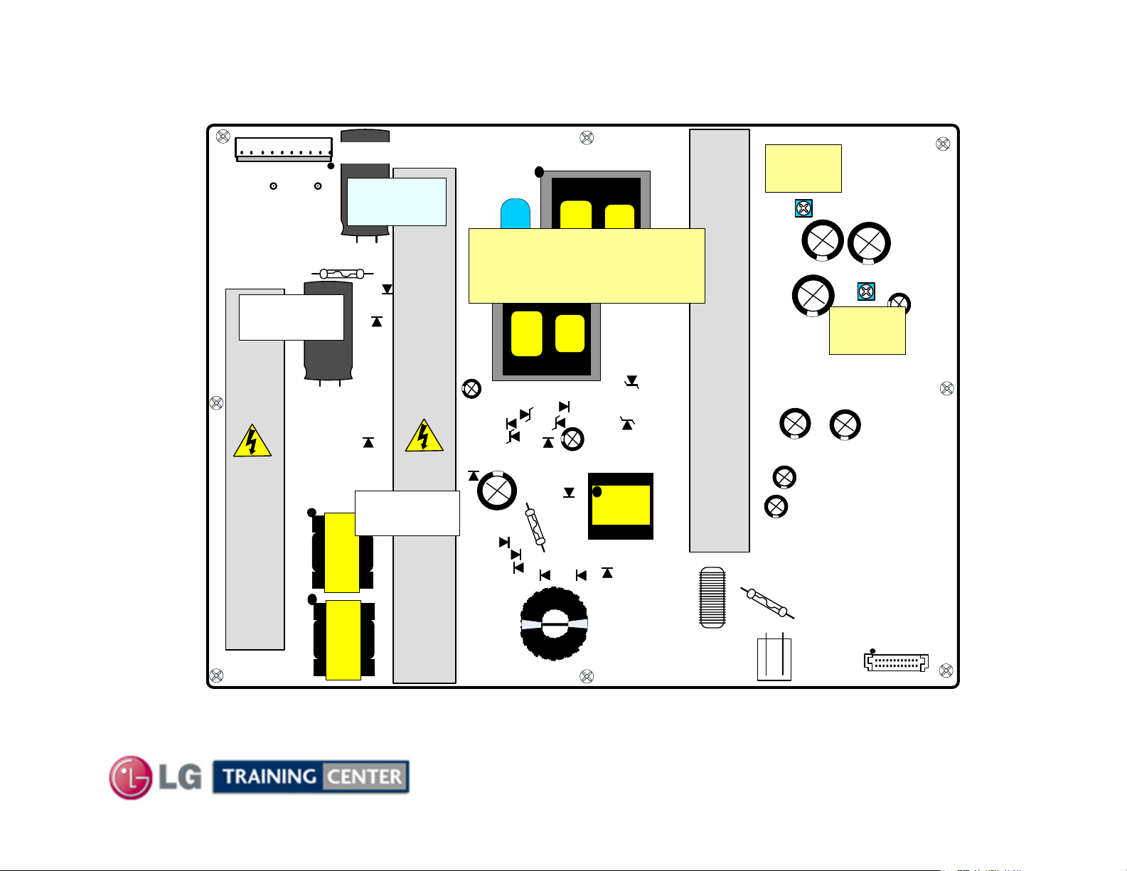
Power Supply Board Layout (Drawing)
Power Supply Board Layout (Drawing)
VA TP
VS TP
F801
4A
250V
Stand-By: 0.9V
Run: 388V
P812
VS and VA
D805
D601
Stand-By: 1.5V
L601
TP
ZD803
Run: 388V
SMPS
p/n: EAY60968701
ZD302
D307
ZD303
D601
D308
D309
D306
D302
D609
ZD301
D303
D305
F302
2.5A
250V
T901
T301
D103
D301
T902
ZD401
ZD101
VR901
VS Adj
VR502
VA Adj
F101
10A
250V
L602
39
P813
SC101
July 2010 50PJ350 Plasma
Page 40
50PJ350 SMPS STATIC TEST UNDER LOAD
50PJ350 SMPS STATIC TEST UNDER LOAD
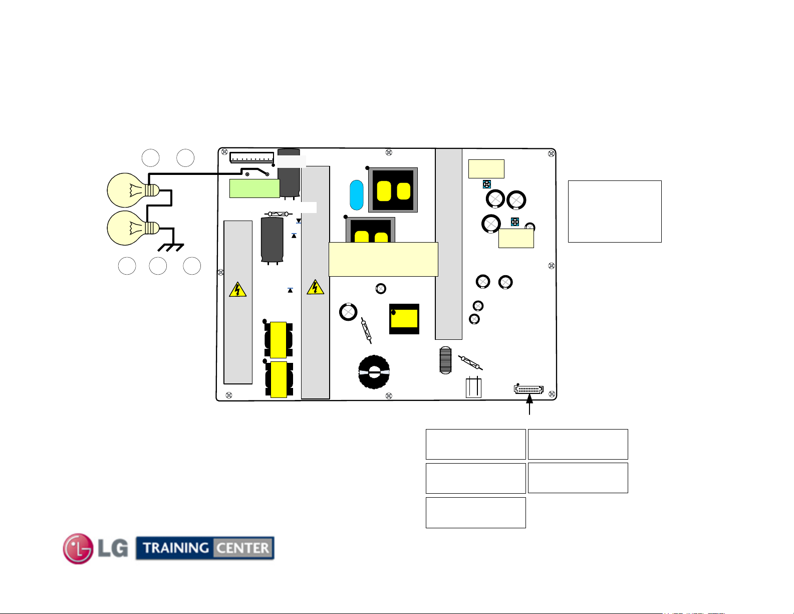
Using two 100 Watt light bulbs, attach one end to Vs and the other end to ground. Apply AC to SC101. If the light bulbs
turn on and VS is the correct voltage, allow the SMPS to run for several minutes to be sure it will operate under load. If
this test is successful and all other voltages are generated, you can be fairly assured the power supply is OK.
Note: To be 100% sure, you would need to read the current handling capabilities of each power supply listed on the silk
screen on the SMPS and place each supply voltage under the appropriate load.
1 2
Pins
100W
100W
4
or
orPins
VS
Gnd
5 8
or
VA VS
Test Points
L601
P812
4A 250V
F801
T901
T902
POWER SUPPLY
p/n: EAY60968701
ZD302
F302
2.5A
250V
D609
ZD401
T301
F101
10A 250V
VR901
VS Adj
VR502
VA Adj
P812
Check Pins 1 or 2
for Vs voltage
Check Pins 6 or 7
for Va voltage
Note:
Always test the SMPS under a
load using the 2 light bulbs.
Abnormal operational
conditions may result if not
loaded.
L602
Note:
To turn on the Power Supply;
1) With Main Board connected, press power.
2) Without Main Board connected SMPS will turn on automatically.
Any time AC is applied to the SMPS, STBY 5V will be 3.46V and will
be 5.14V when the set turns on.
AC DET WILL NOT be present until set comes on.
If AC Det is missing, the TV will come on and shut off in 10 Seconds.
40
SC101
Check Pins 13 or 14
for 5V SBY (5.14V)
Check Pin 8 for
Error Det (4.9V)
Check Pin 16 for
AC Det (4.44V)
July 2010 50PJ350 Plasma
P813
P813
Check Pins 1 or 2 for
17V
Check Pin 5,6 and 7
for (+5V) 5.17V
Page 41
50PJ350 Power Supply Troubleshooting
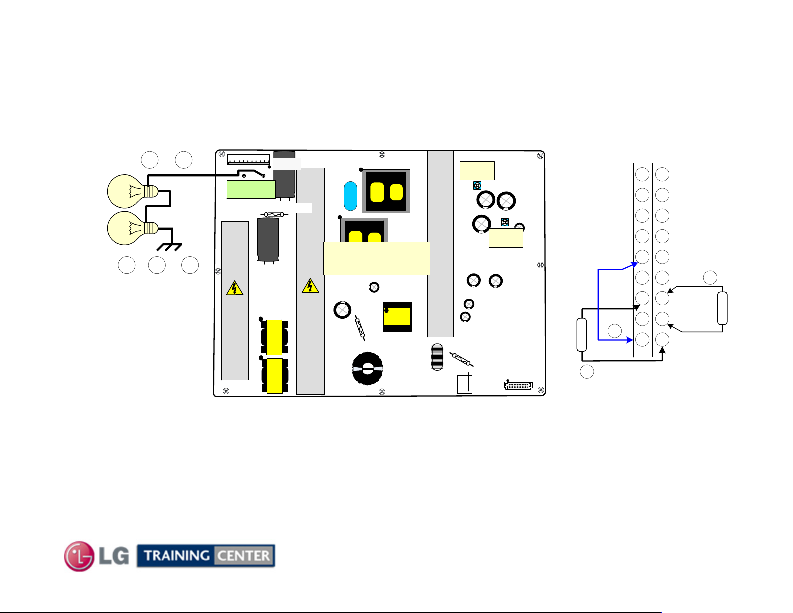
With P813 disconnected from the Main board (P301) attach two 100 Watt light bulbs, attach one end to Vs and the other end to ground.
Apply AC to SC101. If the light bulbs turn on and VS is the correct voltage, allow the SMPS to run for several minutes to be sure it will
operate under load. If this test is successful and all other voltages are generated, you can be fairly assured the power supply is OK.
Note: To be 100% sure, you would need to read the current handling capabilities of each power supply listed on the silk screen on the
SMPS and place each supply voltage under the appropriate load. Then follow the instructions below to completely test turn on sequence.
Note: Placing the two 100 Watt light bulbs from Vs to Ground will assure the power
supply will regulate with a load and no other Abnormal conditions may result.
1 2
Pins
orPins
VS
100W
100W
4
or
Gnd
5 8
or
VA VS
Test Points
P812
4A 250V
F801
T901
T902
POWER SUPPLY
p/n: EAY60968701
ZD302
D609
ZD401
VR901
VS Adj
VR502
VA Adj
17V
Gnd
+5V
Error Det
Gnd
Gnd
STBY
5V
AC Det
A
Auto Gnd
L601
L602
F302
2.5A
250V
T301
F101
10A 250V
P813
100Ω
C
SC101
When the supply is operational in its normal state the Auto Ground line at Pin 18 of P813 is held at ground by the Main Board.
This Power Supply can be powered on sequentially to test the Controller Chip IC701 operational capabilities and for
troubleshooting purposes.
Disconnect P301 from the Main board and use the holes in that end of the connector to insert the jumper and resistors.
Use Main
Board Side
P301
1
2
3
4
5
6
7
8
9
10
11
12
13
14
15
16
17
18
Pin 1
(Front Right)
17V
Gnd
+5V
+5V
Gnd
Gnd
B
STBY
5V
RL
ON
M_On
100Ω
Warning: Remove AC before adding or removing any plug or resistor.
Note: Leave previous installed 100Ω resistor in place when adding the next resistor.
(A) Ground the Auto Gnd Line (Pin 18) will allow the supply to be powered up one section at a time.
(B) Add a 100Ω ¼ watt resistor from 5V Standby to RL_ON and the AC Det, 17V and 5V Lines on P813 will become active.
(C) Add a 100Ω ¼ watt resistor from any 5V line to M_ON (Monitor_On) to make the M5V, VS and VA lines operational.
P812 (VS pins 1 and 2) (VA pins
6 and 7) and (M5V pins 9 and 10).
41
July 2010 50PJ350 Plasma
Page 42
SMPS Connector P813 Identification, Voltages and Diode Check
SMPS Connector P813 Identification, Voltages and Diode Check
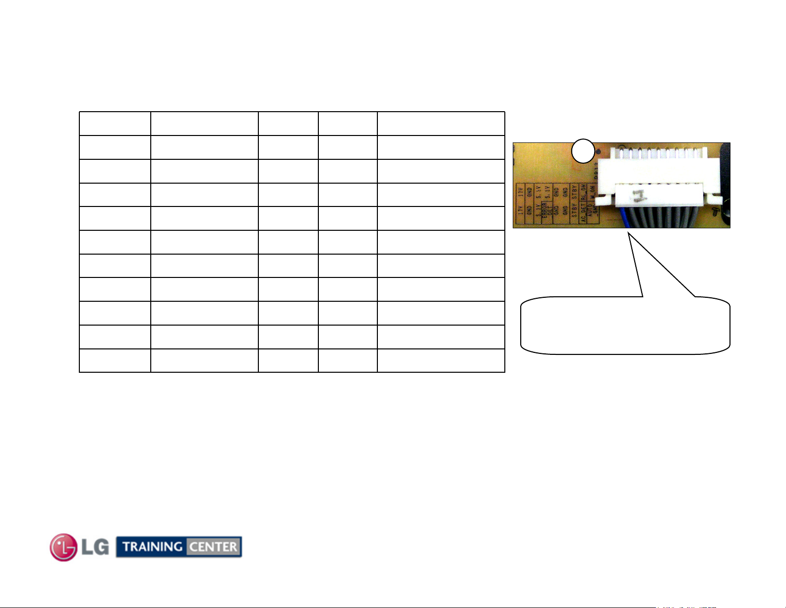
P813 Connector “SMPS" to “Main" P301
Diode ModeRun STBYLabelPin
a
16V1-2
3.17V17V0V
GndGndGndGnd3-4
a c
a
5V5-7
Error Det8
1.16V5.17V0.46V
3.09V4.1V2.85V
GndGndGndGnd9-12
2.55V5.14V3.46VStby 5V13-14
Open2.43V0VRL On15
a d
AC Det16
b
M_ON17
e
Auto Gnd18
a
Note: The 17V, 5V, AC_Det and Error Det turn on when the RL_On command arrives.
b
Note: The M5V, Va and Vs turn on when the M_On (Monitor On) command arrives.
c
Note: The Error Det line is not used in this model.
d
Note: If the AC Det line is Missing, the TV will shut off after 10 seconds of operation.
e
Note: Pin 18 is grounded on the Main board. If this line is floated, the SMPS turns on
Automatically when AC is applied.
3.06V4.44V0V
Open3.29V0V
OpenGndGnd
Note: This connector has two
P813
1
rows of pins.
Odd on bottom row.
Diode Mode Readings taken with all connectors Disconnected. DVM in Diode Mode.
42
July 2010 50PJ350 Plasma
Page 43
SMPS Connector SC101 and P812 Identification, Voltages and Diode
SMPS Connector SC101 and P812 Identification, Voltages and Diode
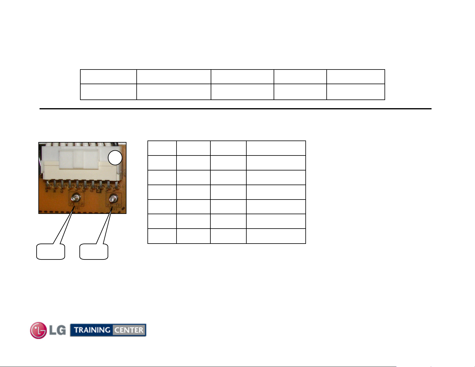
SC101 AC INPUT
Standby Run Diode ModeConnector Pin Number
Check
Check
SC101 120VAC 120VAC Open
P812
Va TP Vs TP
L and N
P812 "Power Supply“ to Y-SUS “P210”
Diode ModeRun LabelPin
1
Open*206V*Vs1, 2
n/cn/cn/c3
GndGndGnd4, 5
Open*60V*Va6, 7
GndGndGnd8
2.16V5VM5V9, 10
* Note: This voltage will vary in accordance with Panel Label
Y-SUS routes Va to bottom X-Left. Vs routed to Z-SUS from P211.
M5V routed through Y-SUS to Control board and then to Z-SUS.
Diode Mode Readings taken with all connectors Disconnected. DVM in Diode Mode.
43
July 2010 50PJ350 Plasma
Page 44

SUS BOARD SECTION
YY--SUS BOARD SECTION
(Overview)
(Overview)
Y-SUS Board develops the V-Scan drive signal to the Y-Drive boards.
This Section of the Presentation will cover alignment and troubleshooting the Y-SUS Board
for the Single Scan Plasma. Upon completion of the Section the technician will have a better
understanding of the operation of the circuit and will be able to locate voltage and
Diode mode test points needed for troubleshooting and alignments.
• Adjustments
• DC Voltage and Waveform Checks
• Diode Mode Measurements
Operating Voltages
Operating Voltages
SMPS Supplied VA
VS
M5V
Y-SUS Developed -VY VR502
VSC VR501
V SET UP VR401
V SET DN VR402
16V
Floating Ground
FG 5V
FG 15V
VA supplies the Panel’s Vertical Electrodes (Routed to the Left X-Board)
VS Supplies the Panel’s Horizontal Electrodes. Also Routed to the Z-SUS board.
M5V Supplies Bias to Y-SUS. (From Y-SUS routed to the Control Board then Z-SUS).
-VY Sets the Negative excursion of Reset in the Drive Waveform
VSC Sets the amplitude of the complex waveform.
SET UP sets amplitude of the Top Ramp of Reset in the Drive Waveform
SET DOWN sets the Pitch of the Bottom Ramp for Reset in the Waveform
Used internally to develop the Y-Drive signal. (Also routed to the Control Board
then routed to the Z-SUS board).
Used on the Y-Drive boards (Measured from Floating Gnd)
Used in the Development of the Y-Drive Waveform (Measured from Floating Gnd)
44
July 2010 50PJ350 Plasma
Page 45
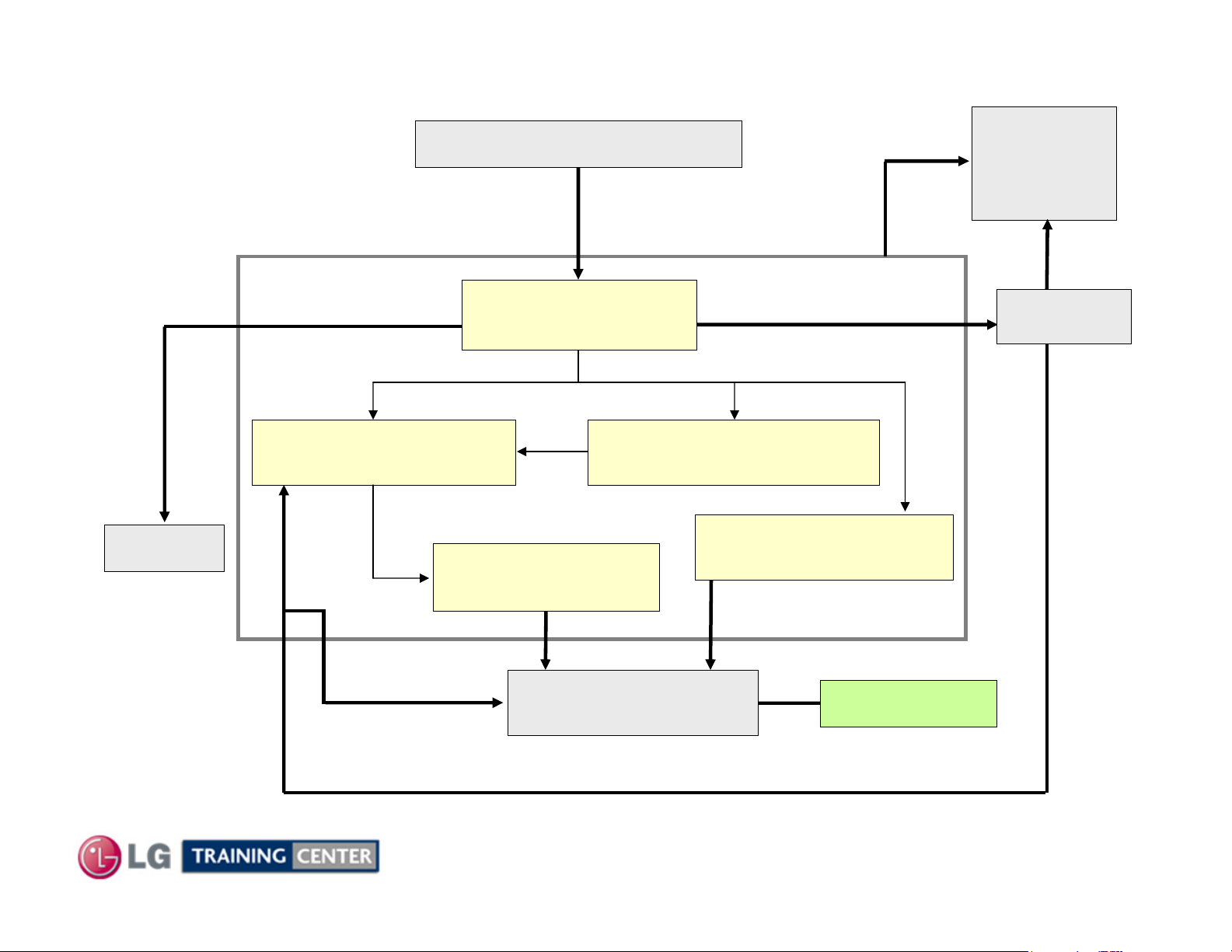
SUS Block Diagram
YY--SUS Block Diagram
Distributes
VA
Left X Board
VA
Power Supply Board - SMPS
Simplified Block Diagram of
Y-Sustain Board
Y-SUS Board
Receive M5V, Va, Vs
from SMPS
Circuits generate
Y-Sustain Waveform
FETs amplify Y-Sustain
Waveform
Distributes Vs
Z-SUS Board
Distributes Vs, Va and M5V
Distributes
16V / M5V
Distributes 16V and M5V
Control Board
Generates Vsc and -Vy
from M5V by DC/DC Converters
Also controls Set Up/Down
Generates Floating Ground
5V/15V by DC/DC Converters
Logic signals needed to
scan the panel
FG5V
Y-Drive Boards
Receive Scan Waveform
Logic signals needed to generate drive waveform
45
July 2010 50PJ350 Plasma
Display Panel
Page 46
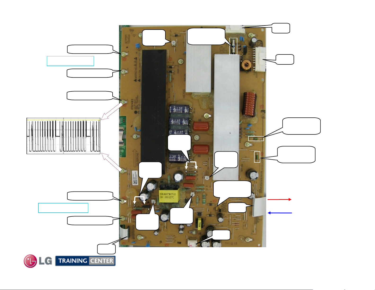
SUS Board Layout
YY--SUS Board Layout
p/n: EBR63039801
Floating Gnd
VR402
Set Up
FS203 (VS)
4A/250V
P211
c
VS to the Z-SUS
To Y-Drive Upper
Floating Gnd
Scan Signal
Floating Gnd
VSC TP
-Vy TP
VR401
Set Dn
FS204 (16V)
2A/125V
c
c
P210
VS, VA and M5V
Input from the SMPS
FS201 (VA)
10A/125V
FS202 (M5V)
10A/125V
16V (pins 1~3)
to Control for Z-SUS
M5V (pins 4-7)
To Y-Drive Lower
Floating Gnd
Logic Signals to
Lower Y-Drive Board
P212
c
VR501
VSC
P101
VR502
-Vy
P203
c
Va to Left X Board Pins 5~7
46
July 2010 50PJ350 Plasma
Ribbon
Logic Signals from
the Control Board
Page 47
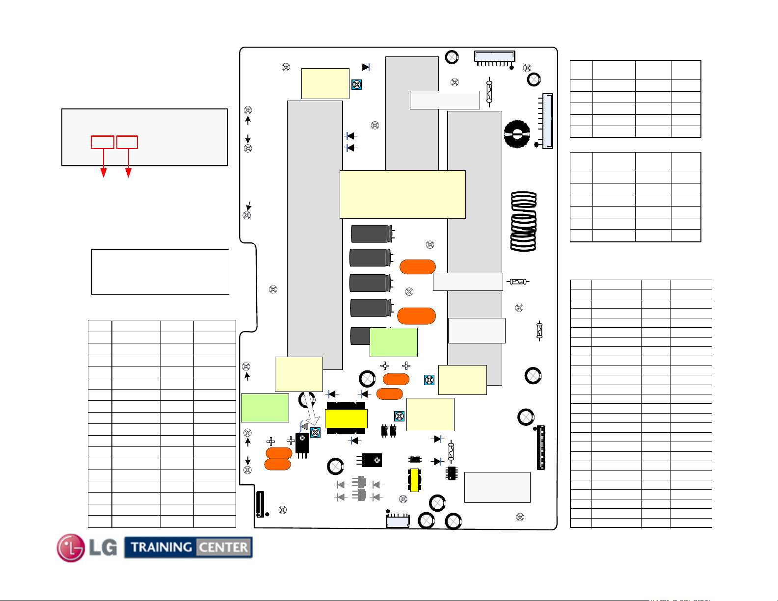
50PJ350 Y-SUS
50PJ350 Y-SUS
Layout Drawing
Layout Drawing
Example:
Model : PDP 50T1###
Voltage Setting: 5V/ Va:60/ Vs:206
N.A. / -198 / 135 / N.A. / 95
Max Watt : 330 W (Full White)
-Vy
VSC
FG
Scan
VR402
Set-Up
D401
FS203 VS
Diode Check reads Open with
Board Disconnected or Connected
D409
D407
Y-SUS BOARD
p/n: EBR63039801
P211
FS203 4A
VS
P210
P211 Connector Y-SUS to Z Drive P2
Pin Label Run
1~2 Gnd Gnd Gnd
3 n/c n/c n/c
4~5 +Vs *206V Open
6 n/c n/c n/c
ER_PASS 98V~102V Open
7~11
P210 Connector Y-SUS to SMPS P813
Pin Label Run
1~2 VS *195V Open
3 n/c n/c n/c
4~5 Gnd Gnd Gnd
6~7 VA *60V Open
Gnd
8
9~10 M5V 5.1V 1.19V
Gnd Gnd
Diode
Check
Diode
Check
WARNING:
Both Y-DRIVE Boards must be
removed completely if P205 /
P204 / P110 is pulled.
P212 Connector Y-SUS to Y-Drive B P205
Pin Label Run Diode Check
1 SUS_DN (FG) FG FG
2 SUS_DN (FG) FG FG
3 YB_OC2 2.63V 1.47V
4 YB_OC2 2.63V 1.47V
5 YT_DATA 0V 1.38V
6 YT_DATA 0V 1.38V
7 YTB_OC1 2.2V 1.47V
8 YTB_OC1 2.2V 1.47V
9 YB_STB 2.8V 1.37V
10 YB_STB 2.8V 1.37V
11 YB_CLK 0.86V 1.38V
12 YB_CLK 0.86V 1.38V
13 SUS_DN (FG) FG FG
14 SUS_DN (FG) FG FG
15 FG5V 4.9V 1.82V
16 FG5V 4.9V 1.82V
17 SUS_DN (FG) FG FG
Scan
FG
VSC
TP
P212
VR501
VSC
ZD501
VSC
TP
Q502
VSC
D513
D514
D504
T302
D502
IC508
2
1
3
2
1
3
IC509
D503
IC503
Q503
P203
-Vy
TP
-VY
TP
IC502
D511
D512
Board Disconnected o r Connected
VR502
-Vy
D501
IC302
T502
D515
FS201 Va
Diode Check reads Open with
FS202 M5V
Diode Check reads
0.97V Board Connected
or 1.19 Disconnected
VR401
Set-Dn
FS204 2A
16VDC
FS204 Protects 16V Creation
D501 and IC501.
Diode Check 1.61V
With Board Disconnected or
1.59V Connected
FS201 10A
VA
FS202
10A
5VDC
P101
P101 Connector Y-SUS to Control P111
Pin Label Run Diode Check
1~3 +15V 16V 1.61V
4~7
8 Gnd Gnd Gnd
9 CTRL_OE 0V 1.54V
10 Gnd Gnd Gnd
11 OE 0V 1.75V
12 Gnd Gnd Gnd
13 Gnd Gnd Gnd
14 OC2 1.78V 1.19V
15 Delta_VY_Det 2.08V 1.18V
16 DATA 0V 1.02V
17 SET_ON 2.09V 1.14V
18 OC1 1.43V 1.14V
19 Det_Level_Sel 0.03V 1.14V
20 STB 1.97V 1.14V
21 Slope_Rate_Sel 1.34V 1.14V
22 CLK 0.59V 1.14V
23 YER_DN 0V 1.14V
24 SET_UP 0.24V 1.14V
25 YSUS_DN 0.95V 1.14V
26 Ramp_Slope 1.01V 1.14V
27 YER_UP 0.62V 1.14V
28 Y_Pass_Top 1.08V 1.14V
29
30 Gnd Gnd Gnd
+5V 4.9V 1.19V
YSUS_UP
0.06V 1.14V
47
July 2010 50PJ350 Plasma
Page 48
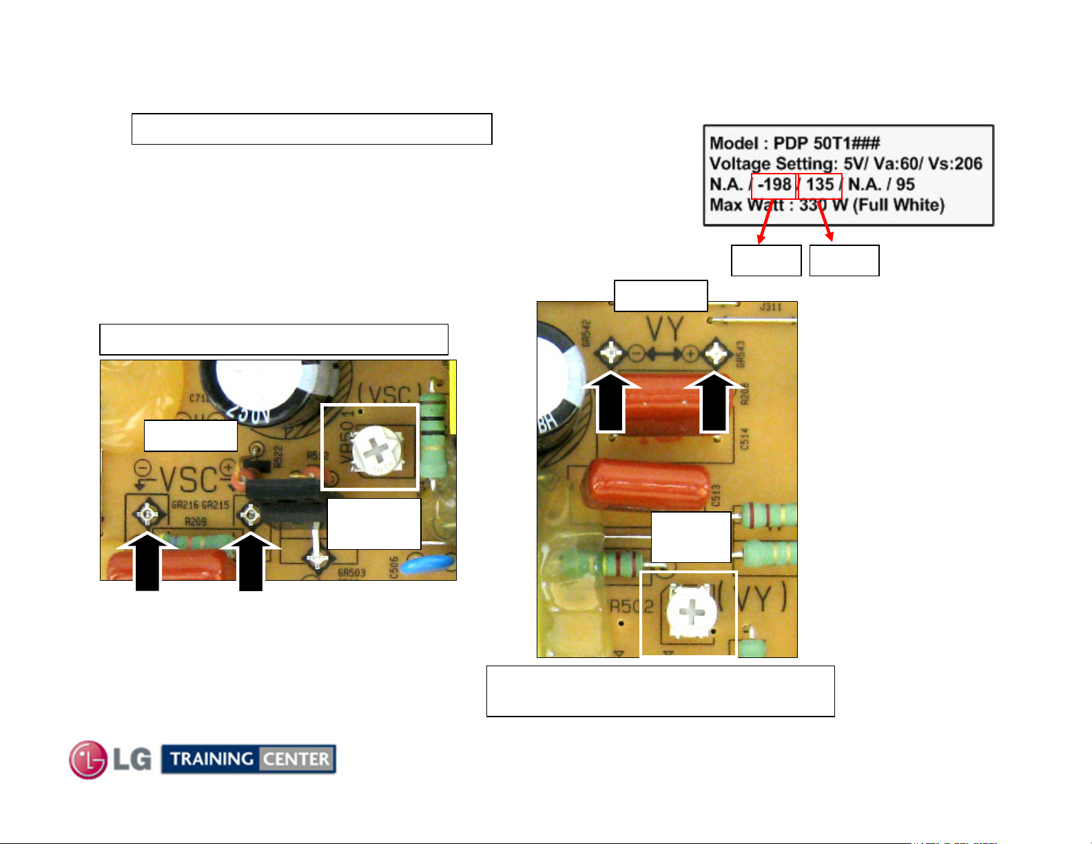
VSC and --
VSC and
Set should run for 15 minutes, this is the “Heat Run” mode.
Set screen to “White Wash”.
1) Adjust –Vy VR502 to Panel’s Label voltage (+/- 1V)
2) Adjust VSC VR501 to Panel’s Label voltage (+/- 1V)
Location: Bottom Left of the board
VY Adjustments
VY Adjustments
These are DC level Voltage Adjustments
CAUTION: Use the actual panel label and not the book for exact voltage settings.
This is just for example
-Vy VSC
-Vy TP
VSC TP
-
Voltages Reads
Positive
+
VR501
VSC Adj
-
VR502
-Vy Adj
Location: Bottom Center of board
Just above Transformer
48
July 2010 50PJ350 Plasma
+
Page 49
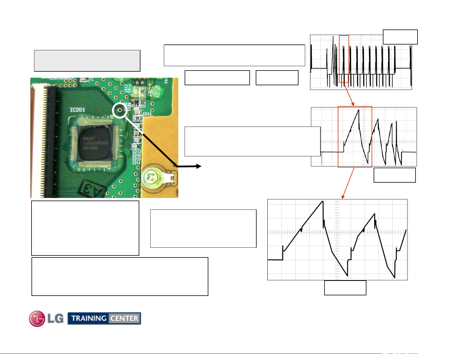
Drive Signal Overview
YY--Drive Signal Overview
2MSec
Y-Drive Lower Test Point
(Top Buffer)
NOTE: The Waveform Test
Points are fragile. If by
accident the land is torn and
the run lifted, make sure
there are no lines left to right
in the screen picture.
c Overall signal observed 2mS/div
75 to 90 VRMS
White to Black
548V p/p
d Highlighted signal from waveform
above observed 200uS/div
e Highlighted signal from
waveforms above observed
100uS/div
200uSec
There are several other test points on either the
Upper or Lower Y-Drive boards that can be used.
Basically any output pin on any of the FPC
to the panel are OK to use.
49
100uSec
July 2010 50PJ350 Plasma
Page 50
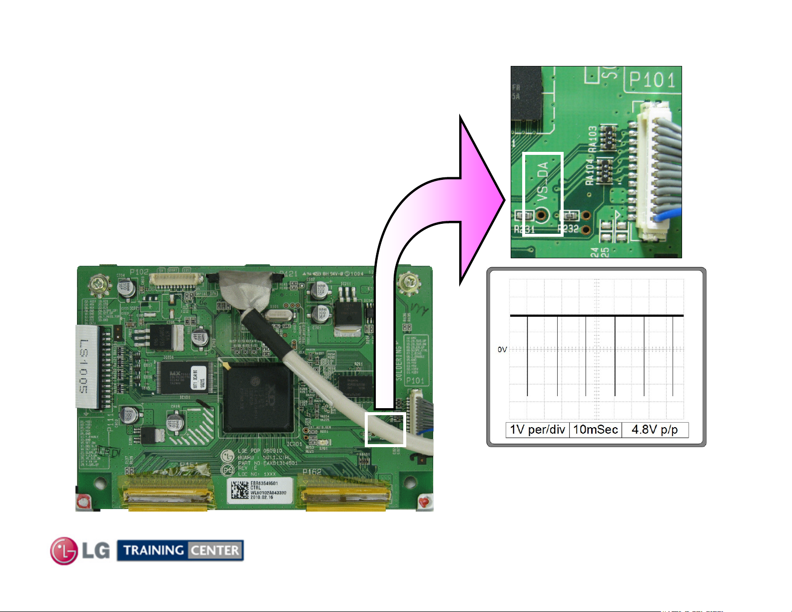
Locking on to the Y--
Locking on to the Y
Note, this TP (VS_DA) can be used as an
External Trigger for scope when locking onto
the Y-Drive (Scan) or the Z-Drive signal.
This signal can also be used
to help lock the scope when observing
the LVDS video signals.
Drive Waveform Tip
Drive Waveform Tip
50
July 2010 50PJ350 Plasma
Page 51
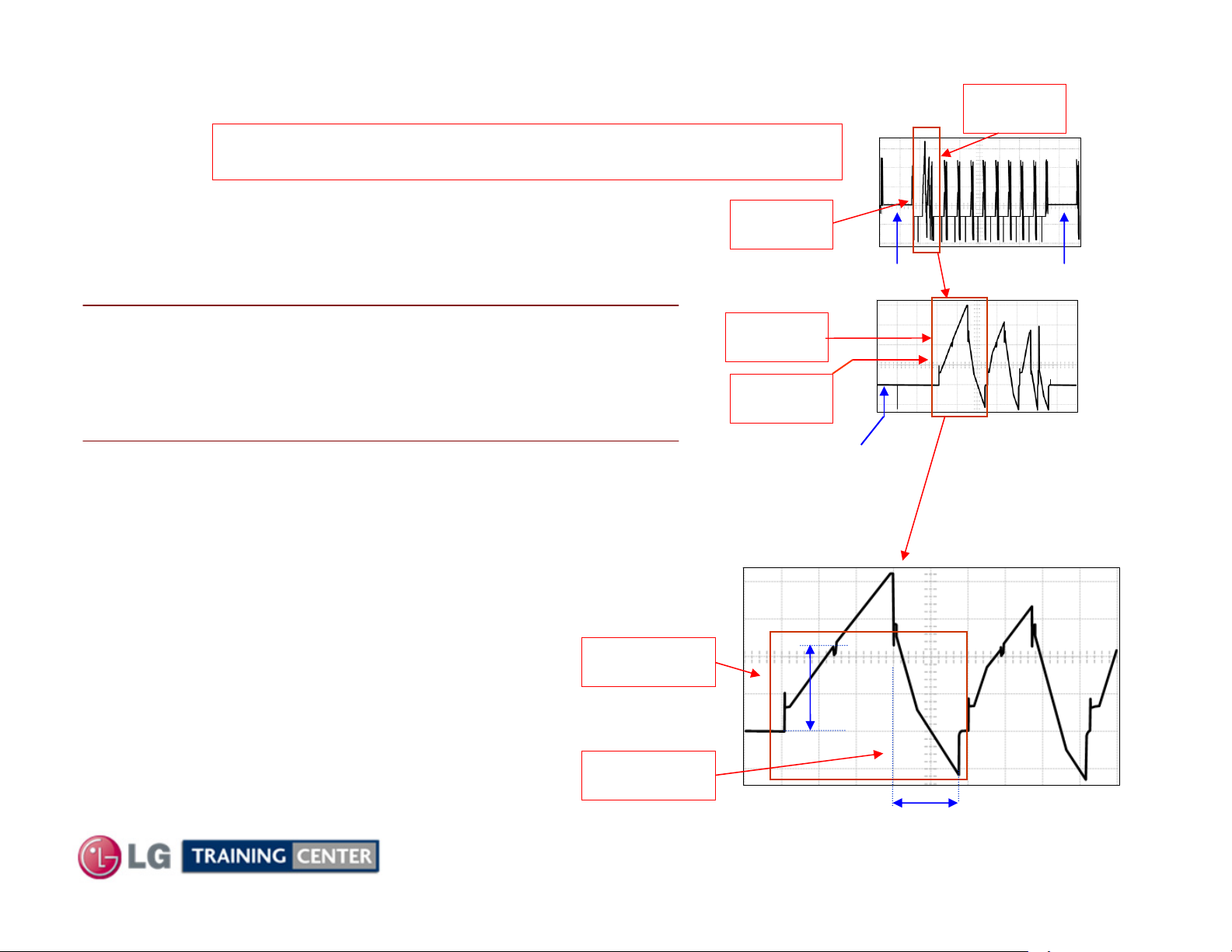
Observing (Capturing) the Y--
Observing (Capturing) the Y
Set must be in “WHITE WASH”
All other DC Voltage adjustments should have already been made.
Drive Signal for Set Up Adjustment
Drive Signal for Set Up Adjustment
Fig 1:
As an example of how to lock in to the Y-Drive Waveform.
Fig 1 shows the signal locked in at 2ms per/div.
Note the 2 blanking sections.
The area for adjustment is pointed out within the Waveform
Area to
expand
Adjustment
Area
FIG1
2mS
Blanking Blanking
Fig 2:
At 200uSec per/division, the area of the waveform to
use for SET-UP or SET-DN is now becoming clear.
Now the only two blanking signals are present.
Fig 3:
At 100us per/div the area for adjustment of SET-UP or SET-DN
is now easier to recognize. It is outlined within the Waveform.
Remember, this is the 1
TIP: If you expand to
adjustment for:
st
large signal to the right of blanking.
100uSec per/division, the
Area for Set-Up
adjustment
SET-UP can be made using VR402 and the
SET-DN can be made using VR401.
It will make this adjustment easier if you use the
“Expanded” mode of your scope.
Area for Set-Dn
adjustment
Adjustment
Area
Area to
expand
Blanking
FIG2
200uS
Expanded from above
FIG3
100uS
Expanded from above
224V
p/p
51
180 uSec
July 2010 50PJ350 Plasma
Page 52
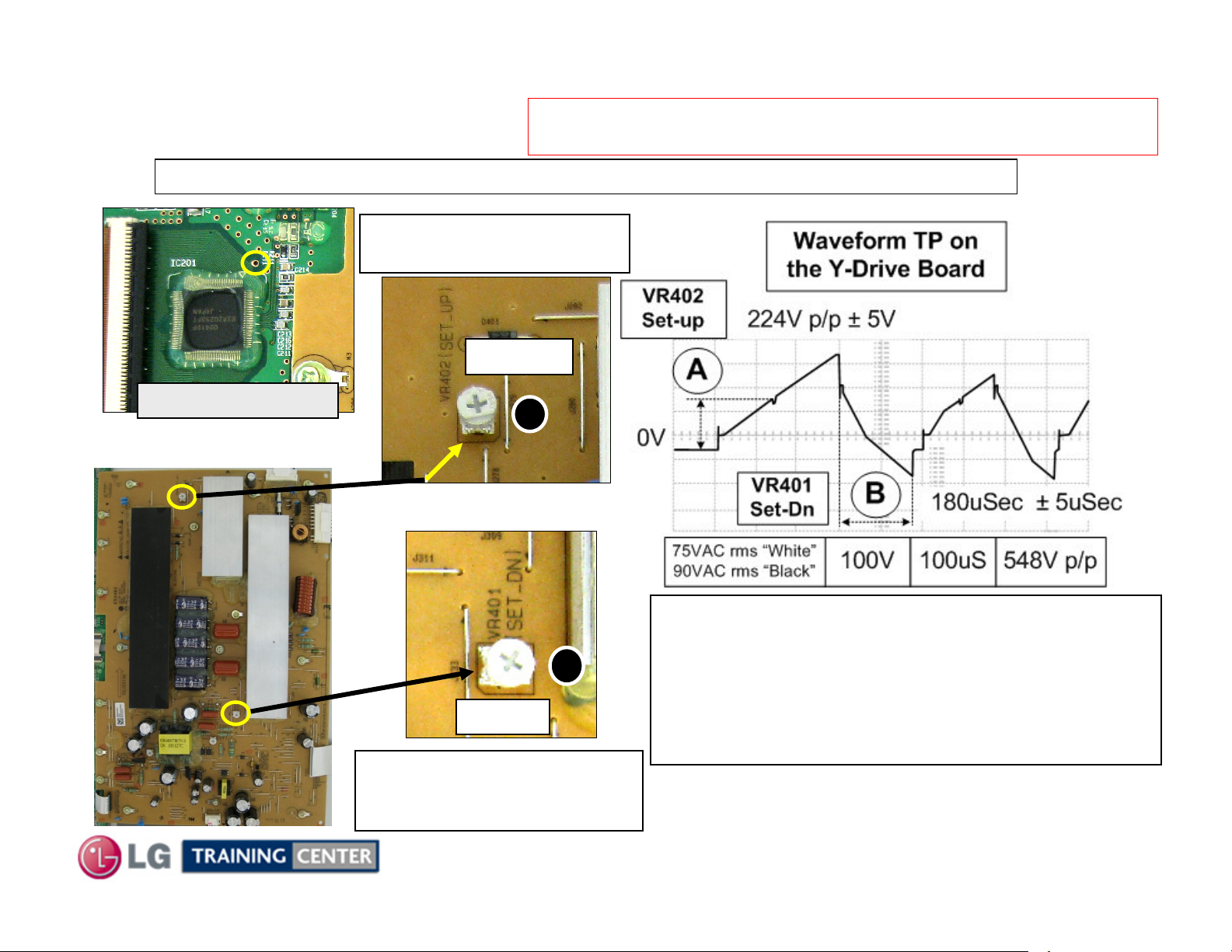
Set Up and Set Down Adjustments
Set Up and Set Down Adjustments
Observe the Picture while making these adjustments. Normally, they do not have to be done.
ADJUSTMENT LOCATION:
Top Left of the board.
VR402
Set must be in “WHITE WASH”
All other DC Voltage adjustments should have already been made.
Y-Drive Test Point
Lower Y-Drive Top Buffer
A
B
VR401
ADJUSTMENT LOCATION:
Lower Center Right
of the board.
SET-UP ADJUST:
1) Adjust VR402 and set the (A) portion of the signal to
match the waveform above. (224V p/p ± 5V)
SET-DN ADJUST:
2) Adjust VR401 and set the (B) time of the signal to match
the waveform above. (180uSec ± 5uSec)
52
July 2010 50PJ350 Plasma
Page 53
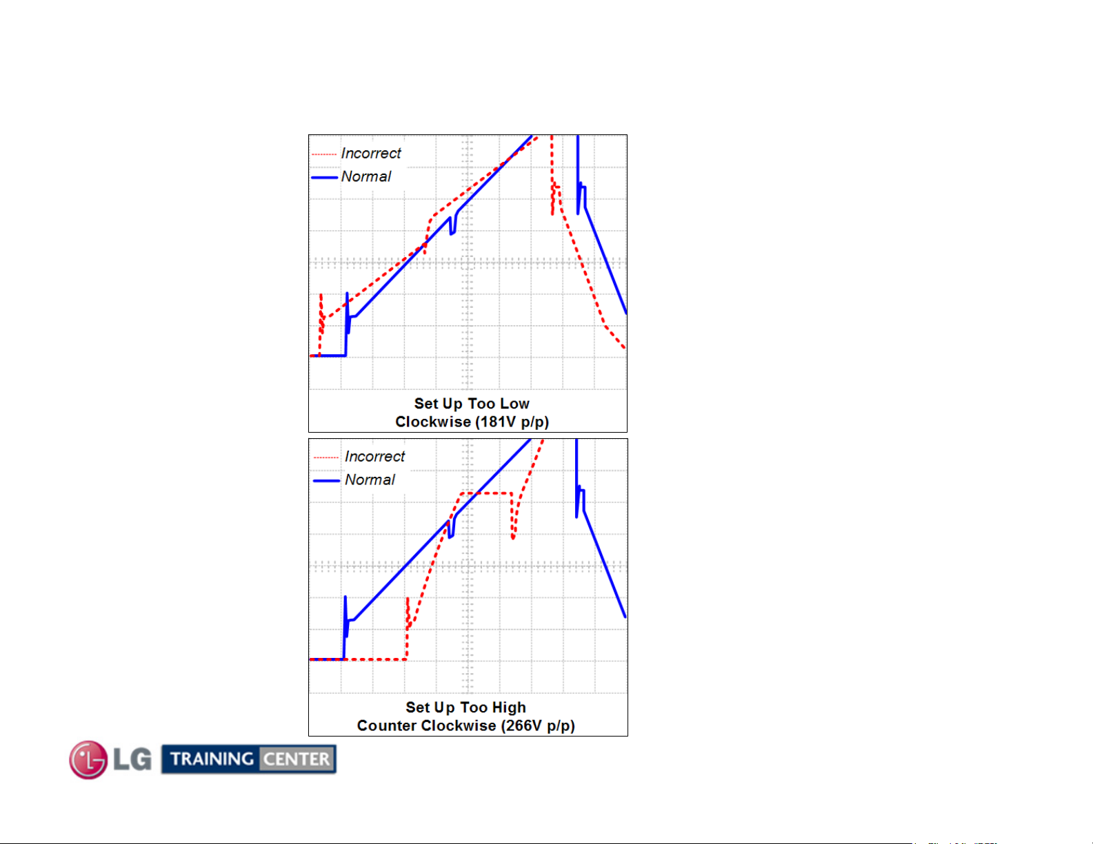
Set Up Adjustment Too High or Low
Set Up Adjustment Too High or Low
Set Up swing is Minimum 181V Max 266V p/p
53
July 2010 50PJ350 Plasma
Page 54
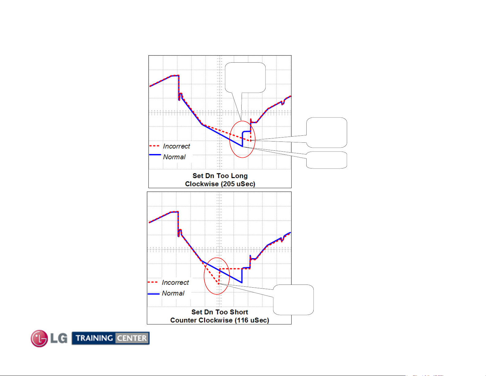
Set Down Adjustment Too High or Low
Set Down Adjustment Too High or Low
Set Dn swing is Minimum 116uSec Max 205uSec
Normal
180uSec
23V off the
Floor
Floor
54
Too Low
116uSec
July 2010 50PJ350 Plasma
Page 55
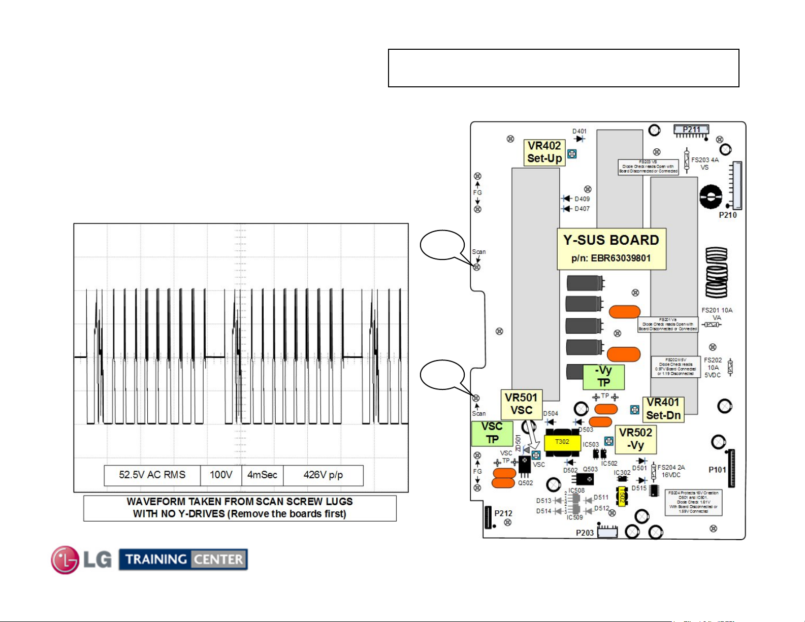
SUS Board Troubleshooting VScan
YY--SUS Board Troubleshooting VScan
TIP: Use the Scan Output Screw Lugs to test for
V-Scan signal if the Y-Drive boards are removed
Y-SUS Board develops the V-Scan drive signal to the
Y-Drive boards.
This Section of the Presentation will cover troubleshooting
the Y-SUS Board.
Warning: Never run the Y-SUS with P212 (Y-SUS) or
P204/P110 (Y-Drives) removed unless the Y-Drive boards
are removed completely. Board Failure will occur.
Scan
Scan
P/N EBR6303801
55
July 2010 50PJ350 Plasma
Page 56
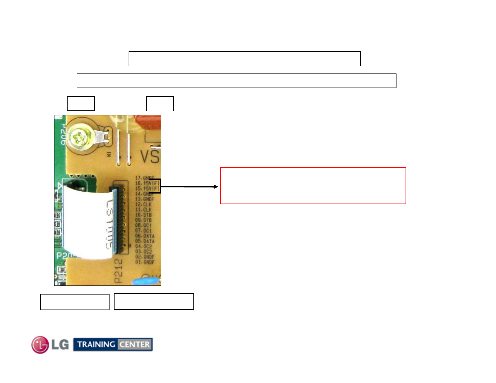
SUS Board P212 Connector to P205 Lower Y
YY--SUS Board P212 Connector to P205 Lower Y
TIP: Connectors do not come with a new Y-SUS or Y-Drives.
TIP: Use Scan Screw Lugs to test for Y-Scan signal if the Y-Drive boards are removed.
Drive (Logic and FG5V)
--Drive (Logic and FG5V)
P205
FGnd
c
P212
FG5V (4.9V) measured from Pins 15 or 16
To Floating Gnd
Use screw just above P212 on the Y-SUS
Y-Drive Lower
Y-SUS Board
56
July 2010 50PJ350 Plasma
Page 57
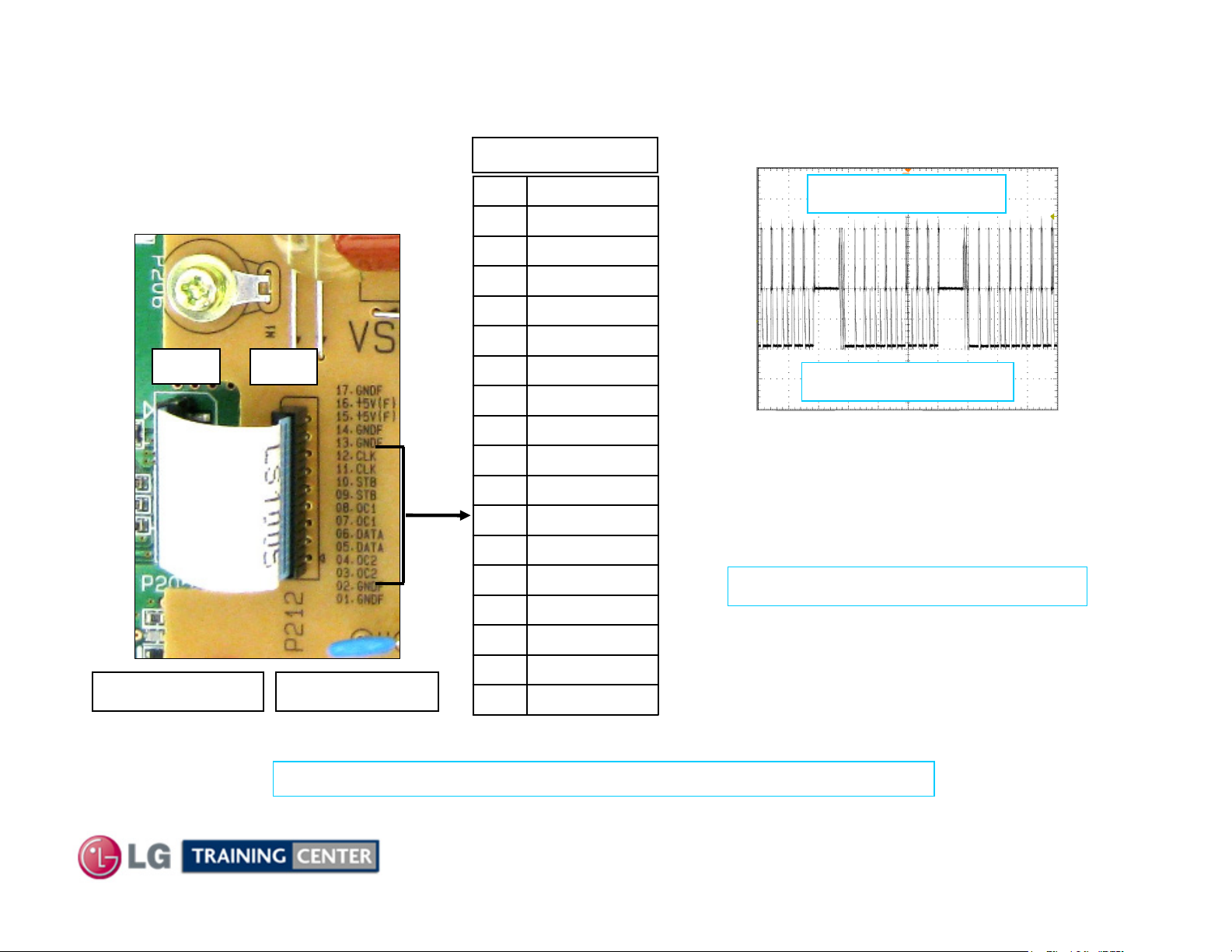
SUS Board P212 to Lower Y--
YY--SUS Board P212 to Lower Y
Drive P205 Logic Signals Explained
Drive P205 Logic Signals Explained
P212 Connector
FGnd
P205
c
c
P212
c
LabelPin
SUS_DN (FG)17
FG5V16
FG5V15
SUS_DN (FG)14
SUS_DN (FG)13
YB_CLK12
Pins 3~12
(4mSec per/div)
YB_CLK11
YB_STB10
YB_STB9
YTB_OC18
YTB_OC17
YT_DATA6
YT_DATA5
YB_OC24
YB_OC23
The signal for these pins look very similar
due to the fact they are read from Chassis Gnd,
but they are actually Floating Ground related.
DO NOT hook scope Gnd to Floating Gnd TP
without an Isolation Transformer.
All logic pins about (400V p/p)
Y-Drive Lower
Y-SUS Board
Pins 3~12 are Logic (Drive) Signals to the Y-Drive Upper.
SUS_DN (FG)2
SUS_DN (FG)1
57
July 2010 50PJ350 Plasma
Page 58
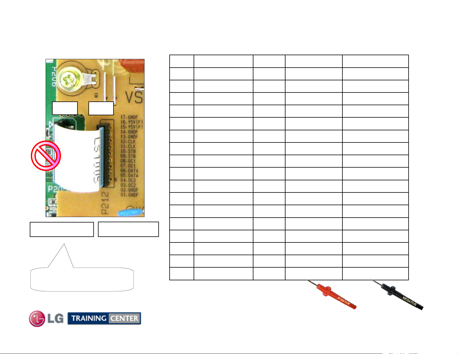
SUS P212 Connector Diode Mode Testing
YY--SUS P212 Connector Diode Mode Testing
FGnd
P205
P212
Meter in the Diode Mode
Red Lead on FGP212 "Y-SUS" to "Lower "Y-Drive" P205
Diode CheckDiode CheckRun LabelPin
FGFGFGSUS_DN (FG)17
0.56V1.82V4.9VFG5V16
0.56V1.82V4.9VFG5V15
FGFGFGSUS_DN (FG)14
FGFGFGSUS_DN (FG)13
0.54V1.38V0.86VYB_CLK12
0.56V1.38V0.86VYB_CLK11
c
c
Y-Drive Lower
Y-Drive Board should be
disconnected for this test.
Y-SUS Board
58
0.66V1.37V2.8VYB_STB10
0.66V1.37V2.8VYB_STB9
0.68V1.47V2.2VYTB_OC18
0.68V1.47V2.2VYTB_OC17
0.54V1.38V0VYT_DATA6
0.55V1.38V0VYT_DATA5
0.68V1.47V2.63VYB_OC24
0.68V1.47V2.63VYB_OC23
FGFGFGSUS_DN (FG)2
FGFGFGSUS_DN (FG)1
July 2010 50PJ350 Plasma
Page 59
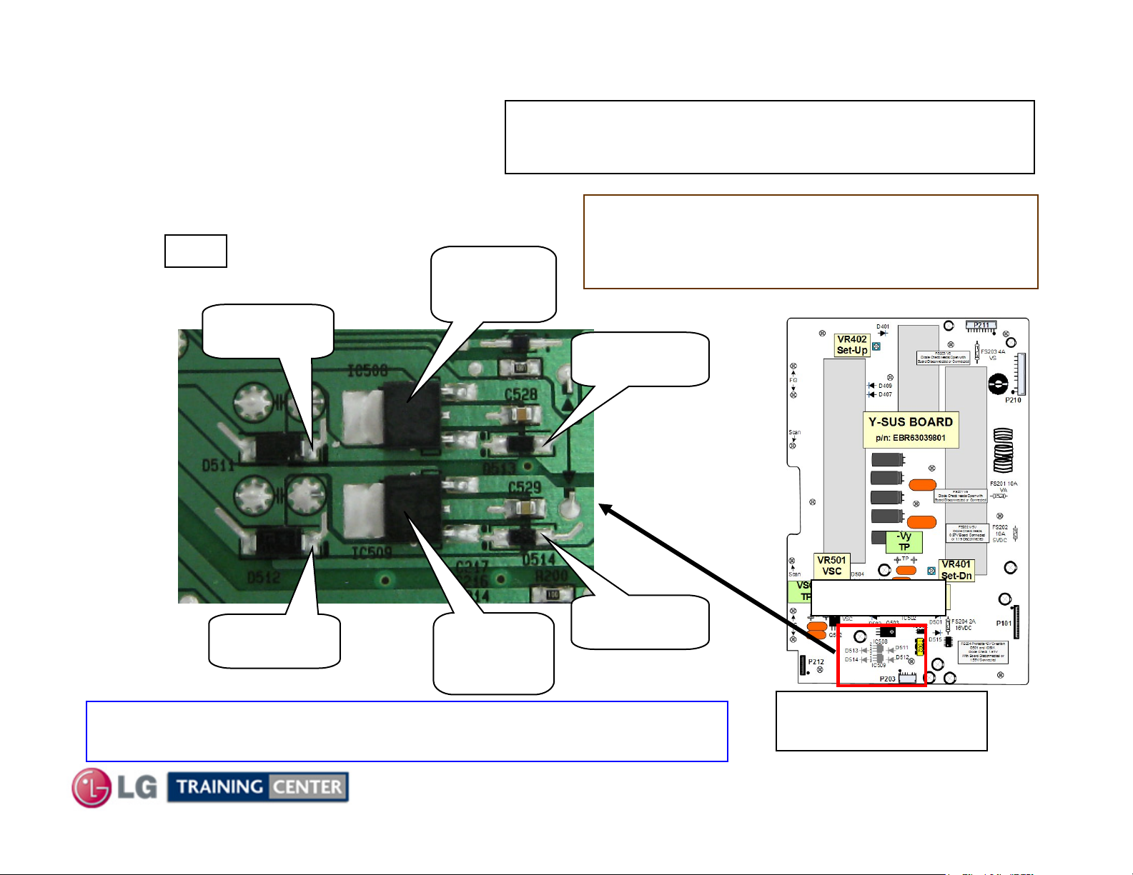
SUS Floating Ground (FG 15V) and (FG 5V) Checks
YY--SUS Floating Ground (FG 15V) and (FG 5V) Checks
Voltage Measurements for the Y-SUS Board
P118
D511
FG 19.86V
FG 15V
Regulator
IC508
TIP: These components are on the back of the board. To Test
these voltages, remove the board completely, supply Ground
and any 5V supply to M5V fuse FS202.
Floating Ground checks must be made from
Floating Ground.
Use bottom two or top two screws on the far left
hand side of the Y-SUS.
D513
FG 15.24V
D514
D512
FG 9.17V
FG5V (Floating Ground 5V). Checked at IC509 Bottom Leg.
FG15V (Floating Ground 15V). Checked at IC508 Bottom Leg.
FG 5V
Regulator
IC509
FG 4.97V
59
Location
Location
Back Side of Board
July 2010 50PJ350 Plasma
Page 60
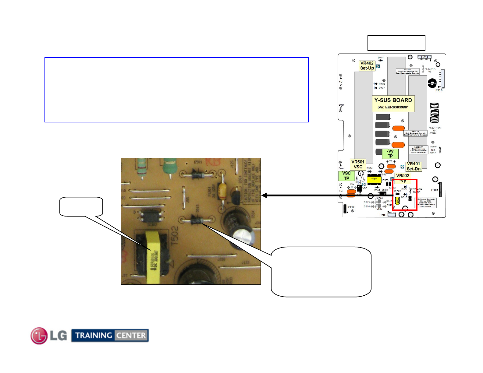
SUS 16V Generation Checks
YY--SUS 16V Generation Checks
Voltage Measurements for the Y-SUS Board
16V Test Point
Used in the Y-SUS for Waveform Creation and Leaves the
Y-SUS board on P101 pins
Checked at Cathode Side D515.
Run: 16VStandby: 0V Diode Check: 1.32V
T502
1~3 to the Control Board.
Location
60
D515
16V Source
Cathode Right Side
Just above T502
July 2010 50PJ350 Plasma
Page 61
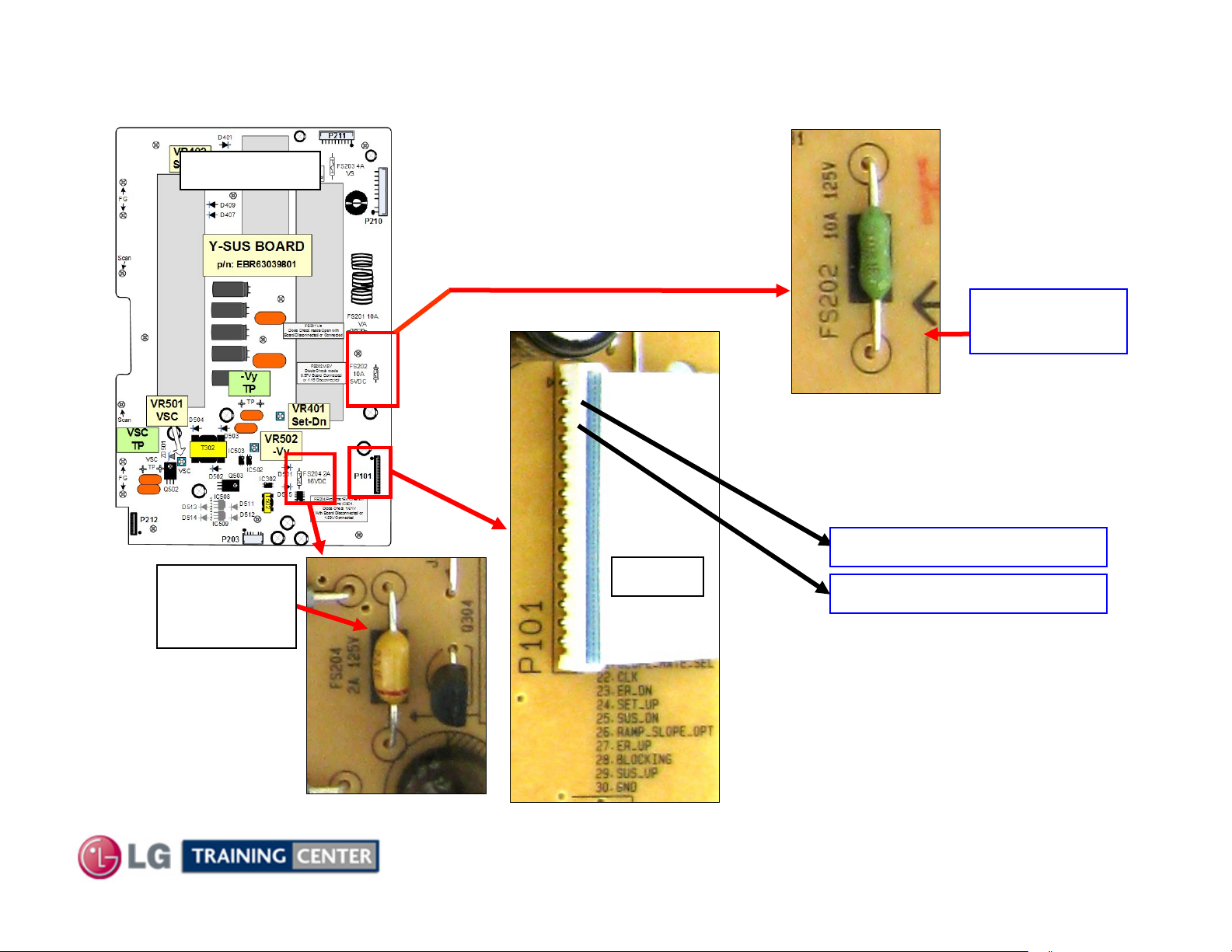
P101 Y--
P101 Y
SUS to Control Board Fuse Information
SUS to Control Board Fuse Information
Locations
FS204
(16V)
2A/125V
c
Diode Check
Open
With Board
Disconnected
or Connected
FS201 (M5V)
10V/125V
Diode Check
1.19V
With Board
Disconnected.
0.97V with board
connected.
16V Pins 1 through 3
P101
M5V Pins 4 through 7
FS204 Protects 16V
Creation
D501 and IC501.
Diode Check 1.61V
With Board
Disconnected or
1.59V Connected
61
July 2010 50PJ350 Plasma
Page 62
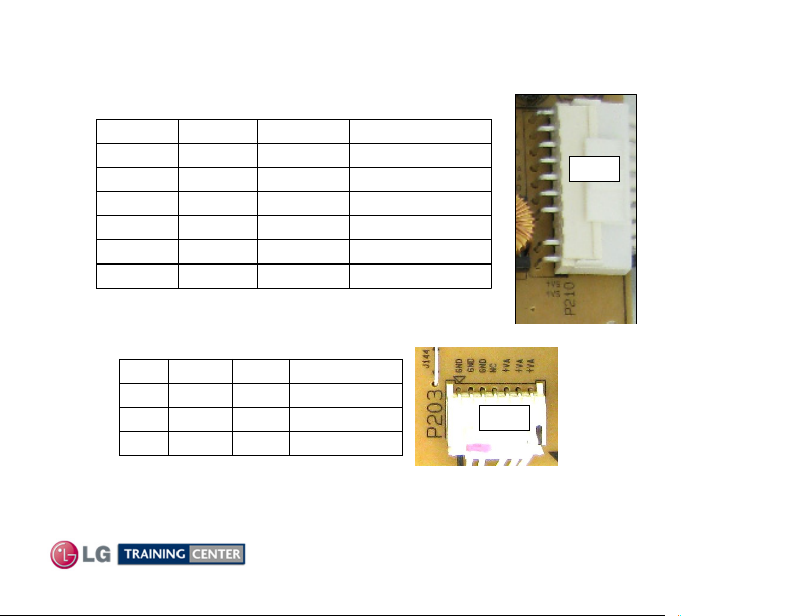
SUS P113 and P114 Plug Information
YY--SUS P113 and P114 Plug Information
P210 Connector "Y-SUS" to "Power Supply" P812
Diode CheckRun LabelPin
Voltage and Diode Mode Measurement
Open*195VVs1~2
P210
n/cn/cn/c3
GndGndGnd4~5
Open*60VVa6~7
GndGndGnd8
1.19V5.1VM5V9~10
P203 "Y-SUS" to "X-Drive Left" P122
Diode CheckRun LabelPin
GndGndGnd1~3
Openn/cn/c4
Open*60VVa5~7
* Note: These voltages will vary in accordance with Panel Label
Diode Mode Readings taken with all connectors Disconnected. DVM in Diode Mode.
c
c
P203
62
July 2010 50PJ350 Plasma
Page 63
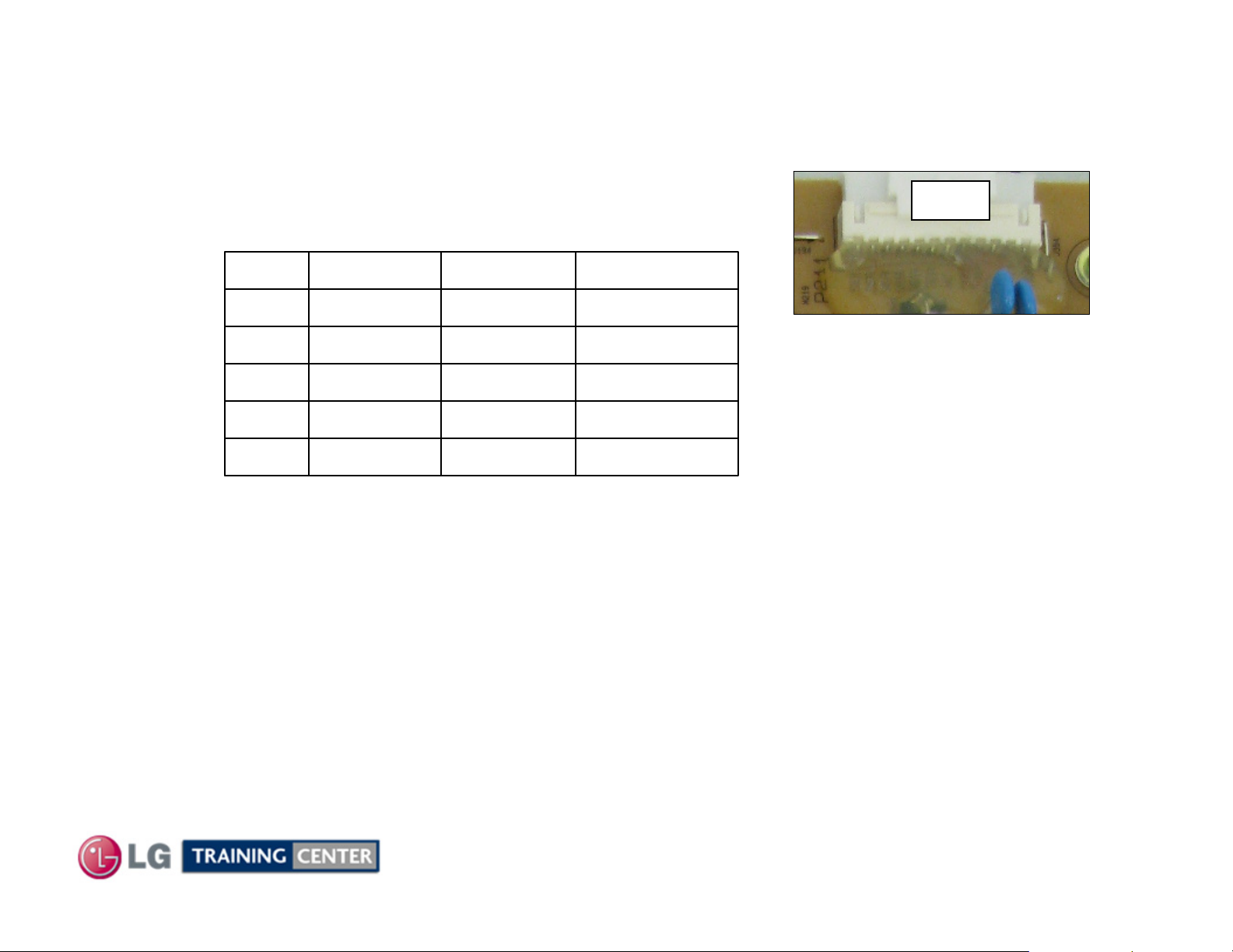
SUS P211 Plug Information
YY--SUS P211 Plug Information
Voltage and Diode Mode Measurement
P211
P211 Connector "Y-SUS" to "Z-SUS" P2
Diode CheckRun LabelPin
GndGndGnd1~2
n/cn/cn/c3
Open*206V*Vs4~5
n/cn/cn/c6
Open98V~102V*ER_PASS7~11
* Note: These voltages will vary in accordance with Panel Label
c
Diode Mode Readings taken with all connectors Disconnected. DVM in Diode Mode.
63
July 2010 50PJ350 Plasma
Page 64
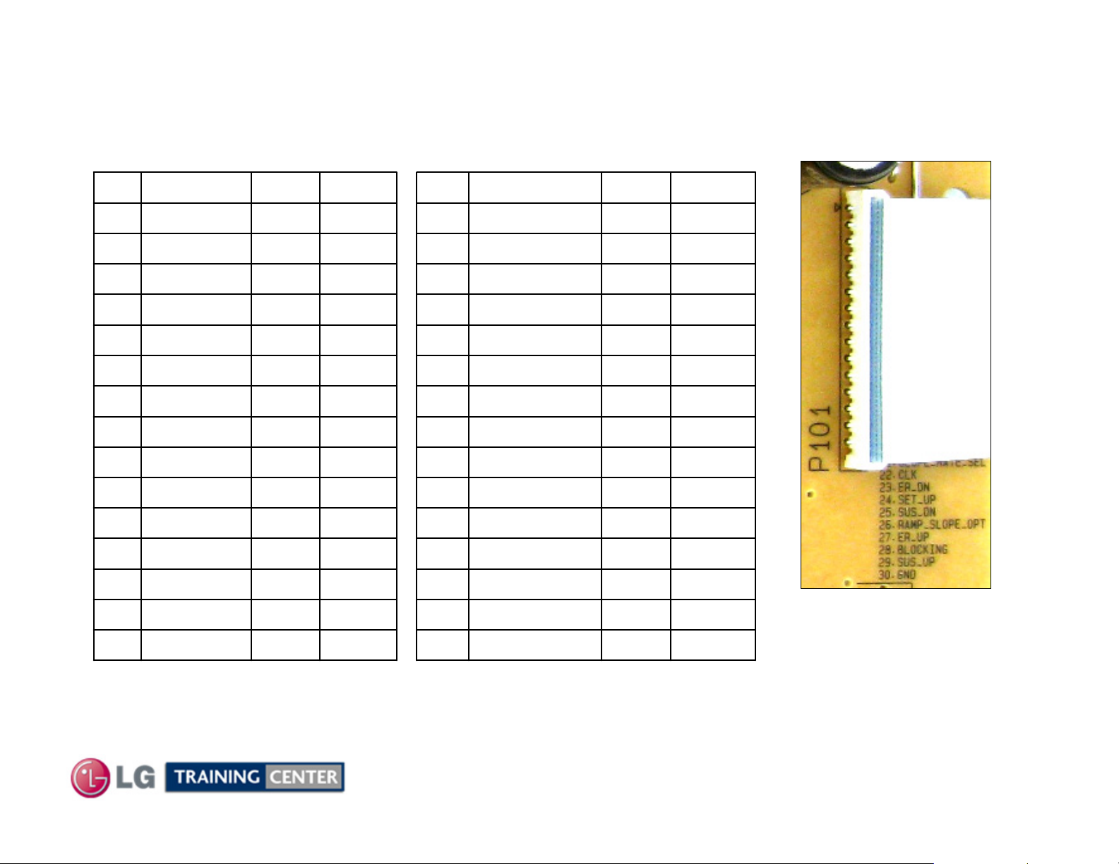
SUS P101 to Control P111 Plug Voltage Checks
YY--SUS P101 to Control P111 Plug Voltage Checks
P101 Connector "Y-SUS" to P111 "Control"
There are No Stand By
Voltages on this Connector
DiodeRunLabelPinDiodeRunLabelPin
15
Delta_VY_Det
1.02V0VDATA161.61V16V+15V1
1.14V2.09VSET_ON171.61V16V+15V2
1.14V1.43VOC1181.61V16V+15V3
191.19V4.9V+5V4
211.19V4.9V+5V6
Det_Level_Sel
Slope_Rate_Sel
1.14V0.03V
1.14V1.97VSTB201.19V4.9V+5V5
1.14V1.34V
1.14V0.59VCLK221.19V4.9V+5V7
1.14V0VYER_DN23GndGndGnd8
1.14V0.24VSET_UP241.54V0VCTRL_OE9
1.14V0.95VYSUS_DN_IN25GndGndGnd10
1.14V1.01VRamp_Slope261.75V0VOE11
1.14V0.62VYER_UP27GndGndGnd12
1.14V1.08VPass_Top28GndGndGnd13
1.14V0.06VYSUS_UP_IN291.19V1.78VOC214
GndGndGnd301.18V2.08V
Diode Mode Readings
taken with all connectors
Disconnected.
DVM in Diode Mode.
c
64
July 2010 50PJ350 Plasma
Page 65
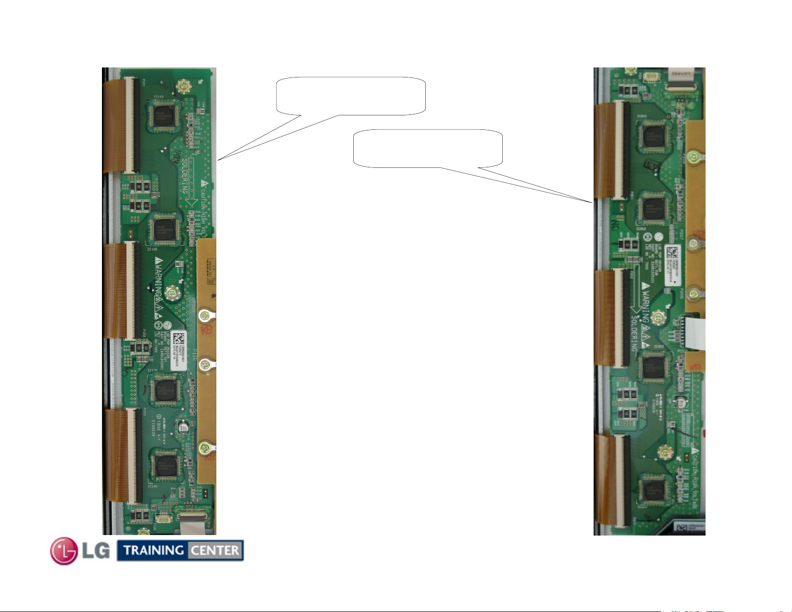
DRIVE BOARD SECTION
YY--DRIVE BOARD SECTION
Y-Drive Boards work as a path supplying the
Sustain and Reset waveforms which are
made in the Y-Sustain board and sent to
the Panel through Scan Driver IC’s.
The Y-Drive Boards receive a waveform
developed on the Y-SUS board then selects
the horizontal electrodes sequentially
starting at the top and scanning down the
panel.
Scanning is synchronized by receiving
Logic scan signals from the Control board.
Drive Explained)
(Y(Y--Drive Explained)
Y-DRIVE UPPER
(TOP)
Y-DRIVE LOWER
(BOTTOM)
The 50PJ350 uses 8 Driver ICs on
2 Y-Drive Boards commonly called
“Y-Drive Buffers” but are actually Gate
Arrays.
65
July 2010 50PJ350 Plasma
Page 66
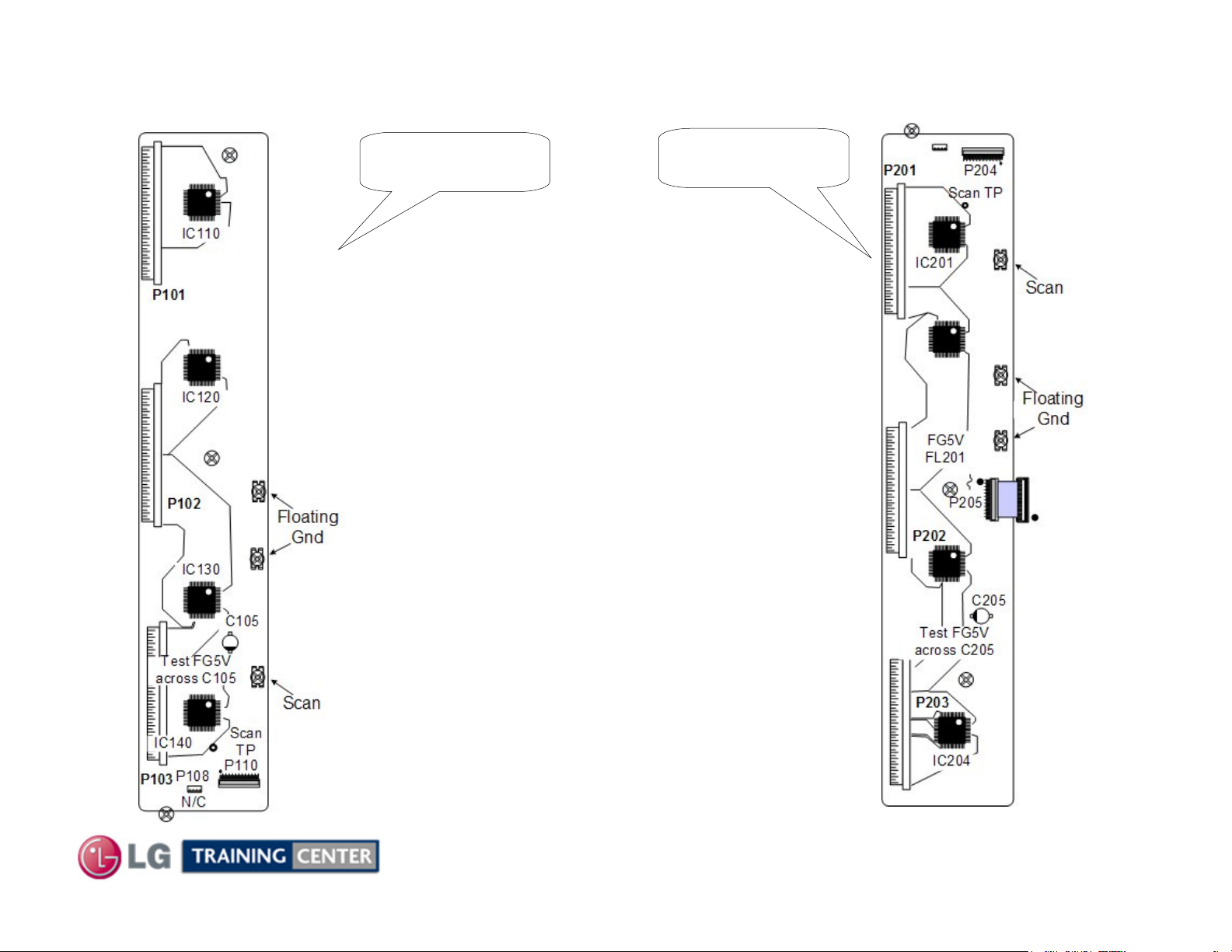
Drive Board Layout
YY--Drive Board Layout
Y-DRIVE UPPER
(TOP)
Key Points of interest are;
If the lugs for Floating Gnd and Scan are
making contact with the Y-SUS board and the
connector P205 or the one between Upper and
lower P204/P110 are removed, the Y-SUS board
will fail.
Floating Ground is delivered to each of the
Y-Drive boards by 2 screw lugs.
Scan is delivered to each of the Y-Drive boards
by 1 screw lugs.
Y-DRIVE LOWER
(BOTTOM)
Each of the Y-Drive boards operate from
Floating Ground, (no reference to Chassis Gnd).
Floating Gnd 5V can be measured across C105
(Upper) or C205 (Lower).
66
July 2010 50PJ350 Plasma
Page 67
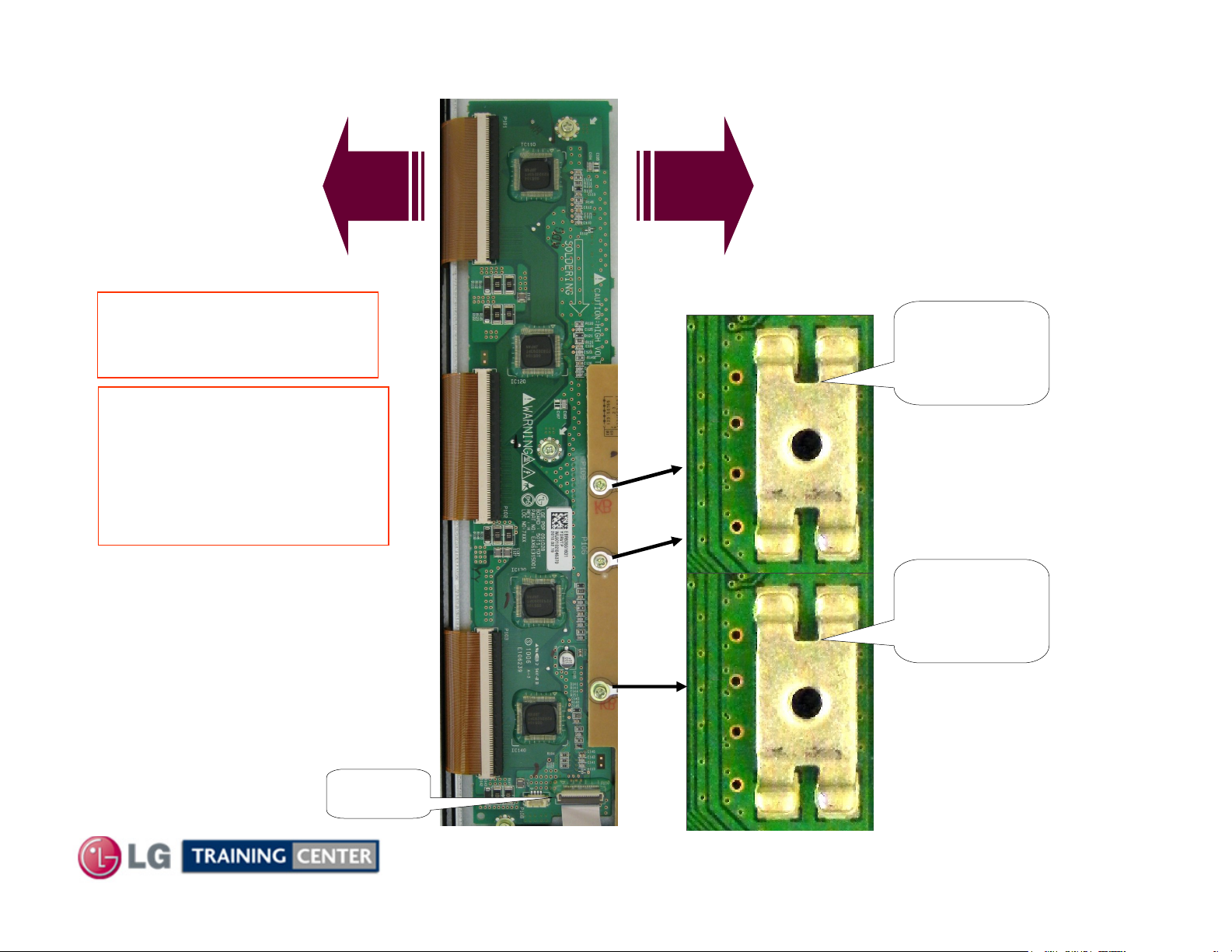
Drive Upper Layout
YY--Drive Upper Layout
PANEL
SIDE
Connector P110 does not
come with a new
Y-SUS or Y-Drive.
Warning: Never run the
Y-SUS with P110
disconnected. You must
remove the Y-Drive board
completely due to these FG
lugs.
Y-SUS
SIDE
p/n: EBR63551601
Y-Drive signal (VSC), FG5V Volts
from the Y-SUS board and Logic
Signals from the Control board
through the Y-SUS are supplied to
the Lower Y-Drive Board on
Connector P205.
Floating
Ground
Standoff
The Floating Ground
Standoff delivers FG
To the Y-Drive Boards.
There are 2 per/board.
P110
67
VScan
The VScan
Standoff delivers the
VScan signal to the
Y-Drive Boards.
There is per/board.
July 2010 50PJ350 Plasma
Page 68
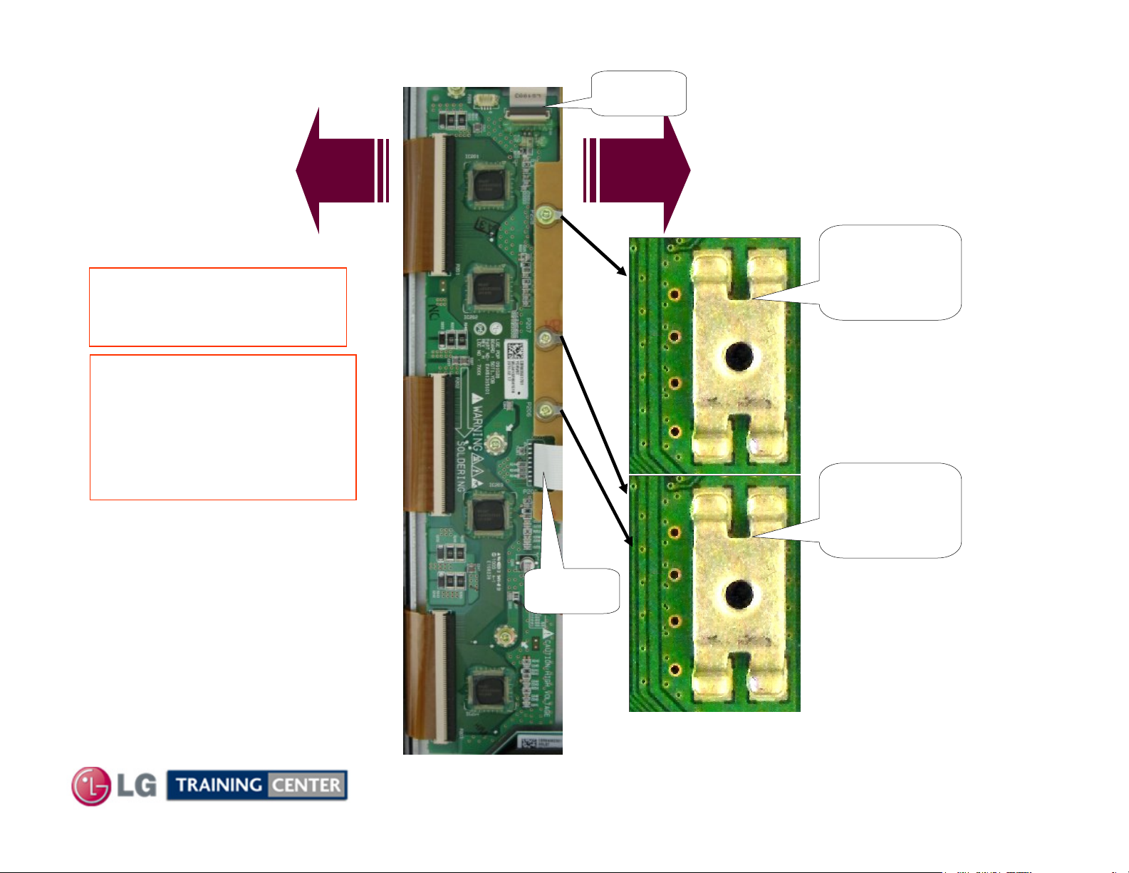
Drive Lower Layout
YY--Drive Lower Layout
P204
p/n: EBR63551701
PANEL
SIDE
Connector P205 or P204
does not come with a new
Y-SUS or Y-Drive.
Warning: Never run the
Y-SUS with P205 or P204
disconnected. You must
remove the Y-Drive boards
completely due to these FG
lugs.
FG5V Volts from the Y-SUS
board and Logic Signals from
the Control board through the
Y-SUS are supplied to the
Lower Y-Drive Board on
Connector P205.
P204 delivers these same
signals to the Upper Y-Drive
P205
Y-SUS
SIDE
VScan
The VScan
Standoff delivers the
VScan signal to the
Y-Drive Boards.
There is per/board.
Floating
Ground
Standoff
The Floating Ground
Standoff delivers FG
To the Y-Drive Boards.
There are 2 per/board.
68
July 2010 50PJ350 Plasma
Page 69
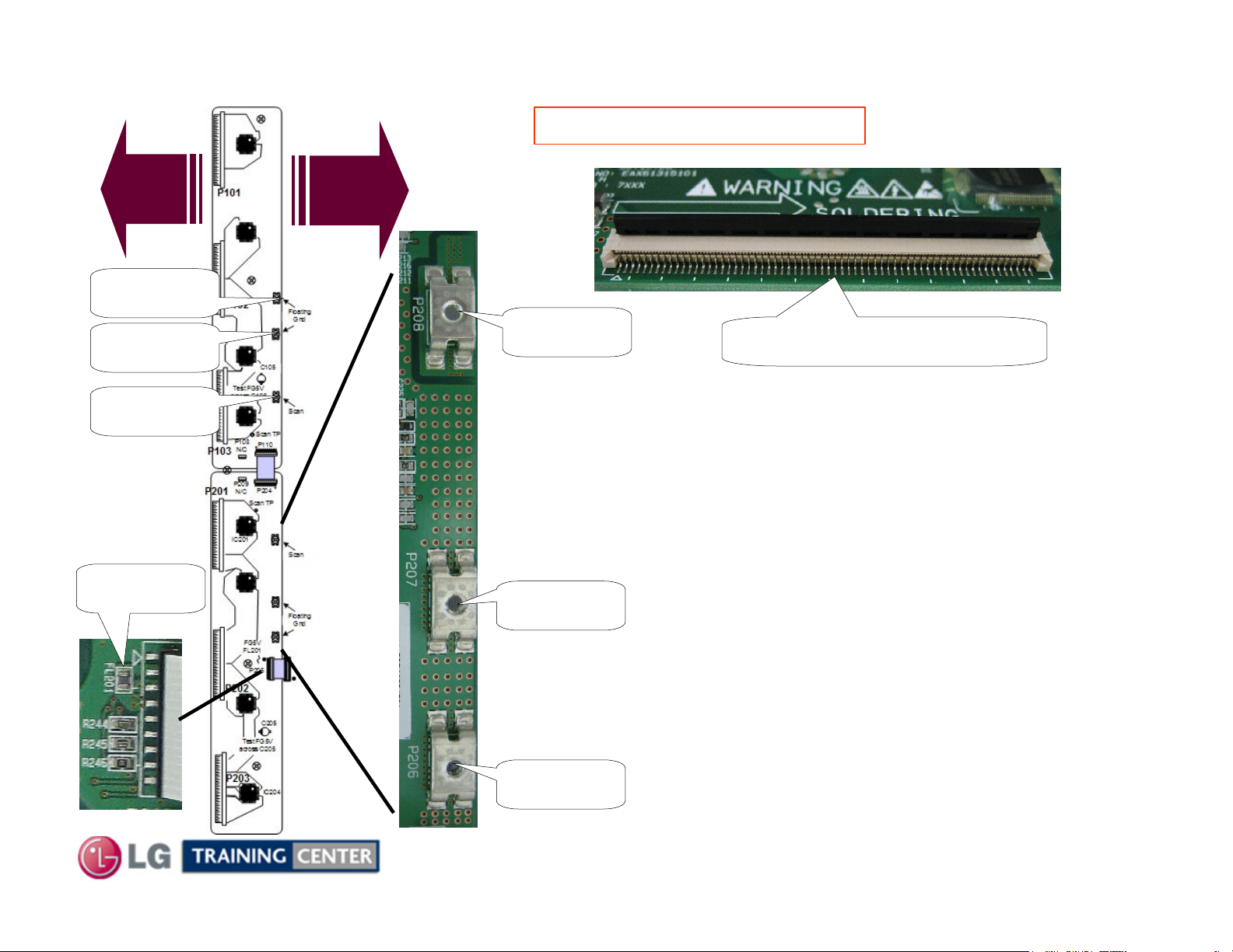
Drive Diode Check Scan and FG
YY--Drive Diode Check Scan and FG
This checks the output Buffers.
PANEL
SIDE
Floating Gnd
Floating Gnd
Scan Signal
FL201
FG5V Fuse
Y-SUS
SIDE
Scan Signal
Floating Gnd
Any Connector to the Panel
(Buffer Output TP)
Diode Mode Reading from Floating Ground
Scan Signal TP
Open with Red Lead on Scan
0.7844V with Black Lead on Scan
FG5V TP
Open with Red Lead on Scan
0.41V with Black Lead on Scan
Floating Gnd
69
Any Output Buffer TP
Open with Red Lead on Scan
0.79V with Black Lead on Scan
July 2010 50PJ350 Plasma
Page 70
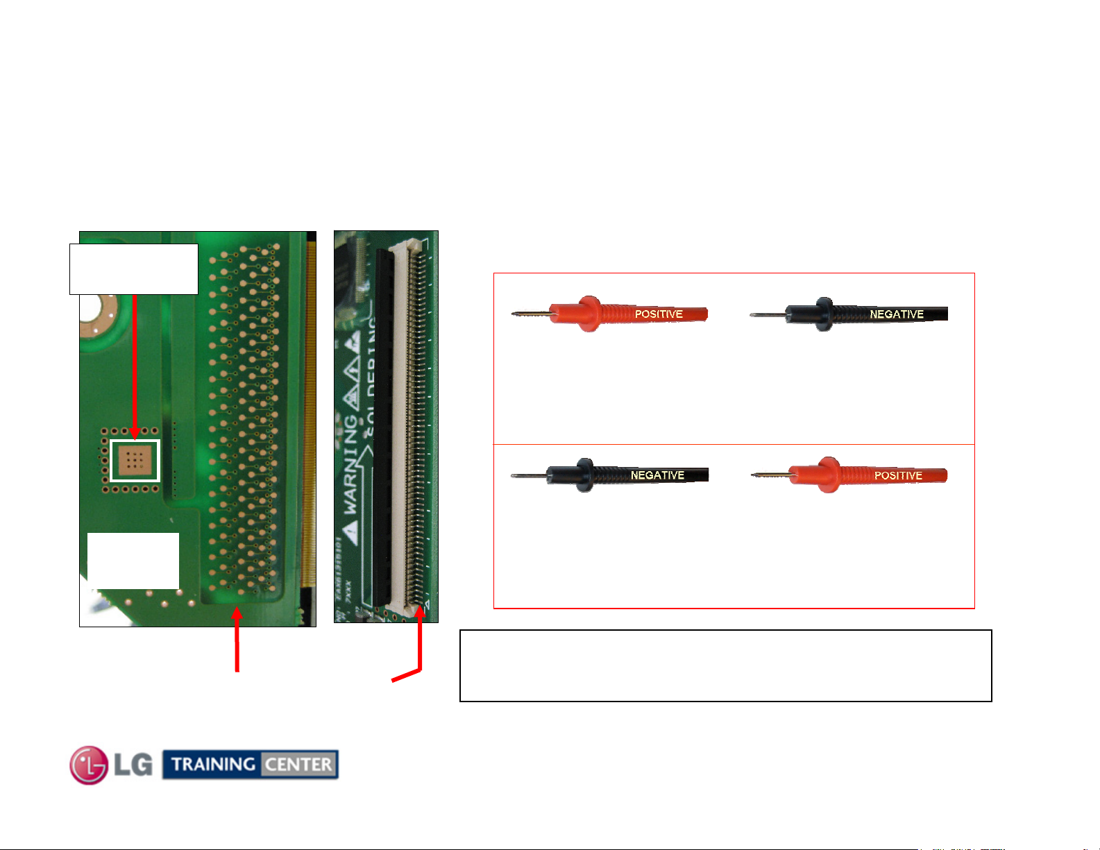
Drive Buffer Troubleshooting
YY--Drive Buffer Troubleshooting
YOU CAN CHECK FOR A SHORTED BUFFER ICs OUTPUT USING THIS PROCEDURERE
YOU CAN CHECK FOR A SHORTED BUFFER ICs OUTPUT USING THIS PROCEDU
BACK SIDE
BUFFER IC
(FGnd)
BACK
SIDE
FRONT SIDE
Using the “Diode Test” on the DVM, check
the pins for shorts or abnormal loads.
RED LEAD On
Floating Ground
Indicated by white outline
BLACK LEAD On
Floating Ground
Indicated by white outline
BLACK LEAD On “ANY”
Output Lug Reads 0.79V
RED LEAD On “ANY”
Output Lug Reads Open
Any of these output lugs can be tested.
Look for shorts indicating a defective Buffer IC
6 Ribbon cables communicating with the Panel’s (Horizontal
Electrodes) totaling 768 lines determining the Panel’s Vertical
resolution pixel count.
70
July 2010 50PJ350 Plasma
Page 71
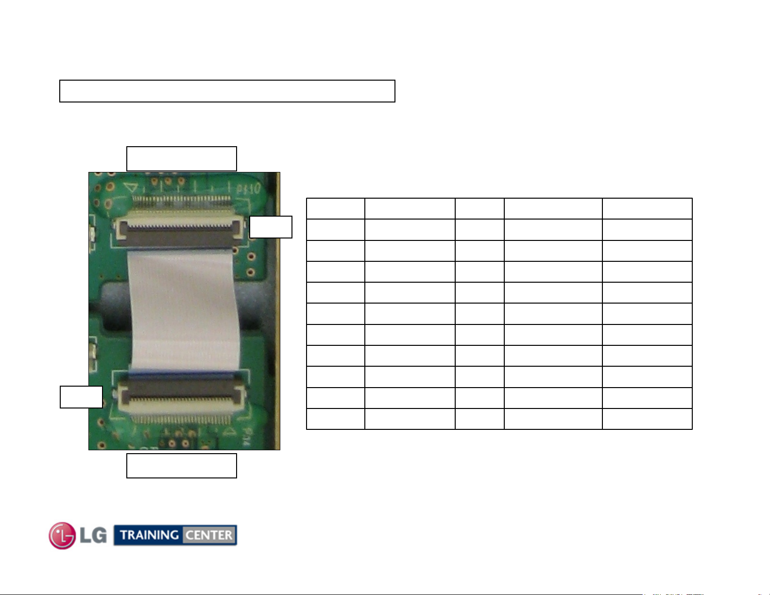
Drive Upper P110 Connector Voltage and Diode Check
YY--Drive Upper P110 Connector Voltage and Diode Check
TIP: This connector does not come with a new Y-Drive.
Y-Drive Upper
P110 "Upper Y-Drive"
Black Lead
on FG
Red Lead
on FG
P204
c
Y-Drive Lower
c
P110
Diode CheckDiode CheckRun LabelPin
FGFGFGSUS_DN (FG)1~10
OpenOpen0VYSUS_DATA11
0.53VOpen2.4VYT_OCR12
0.55VOpen2.2VYT_OC113
0.52VOpen2.6VYT_LE(STB)14
0.52VOpen0.8VYT_CLK15
0.52VOpen0VYT_DATA16
FGFGFGSUS_DN (FG)17~20
0.41V2.8V4.97VFG5V21~23
FGFGFGSUS_DN (FG)24~30
Voltages taken from Floating Ground
Diode Mode Readings taken with all connectors Disconnected. DVM in Diode Mode.
71
July 2010 50PJ350 Plasma
Page 72
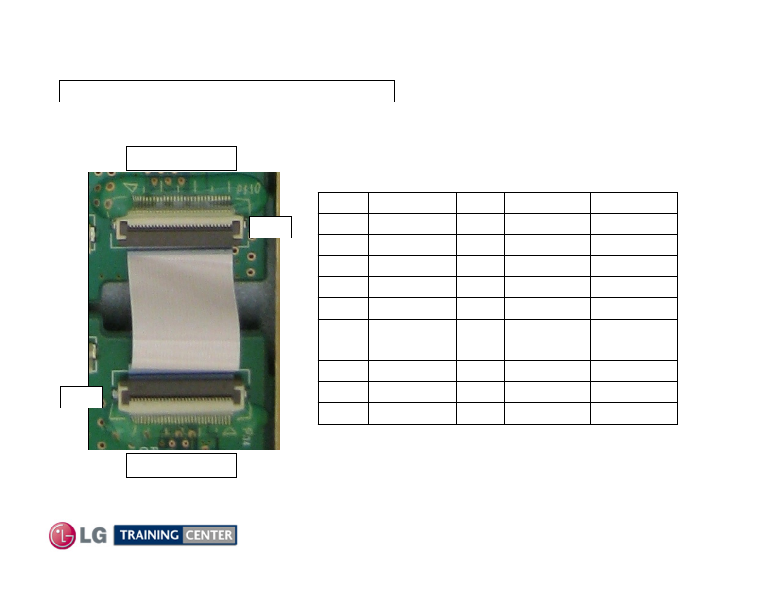
Drive Lower P204 Connector Voltage and Diode Check
YY--Drive Lower P204 Connector Voltage and Diode Check
TIP: This connector does not come with a new Y-Drive.
P204
c
Y-Drive Upper
c
P110
P204 "Lower Y-Drive"
Voltages taken from Floating Ground
Black Lead
on FG
Red Lead
on FG
Diode CheckDiode CheckRun LabelPin
FGFGFGSUS_DN (FG)1~7
0.41VOpen4.97VFG5V8~10
FGFGFGSUS_DN (FG)11~14
0.52VOpen0VYT_DATA15
0.52VOpen0.8VYT_CLK16
0.52VOpen2.6VYT_LE(STB)17
0.55VOpen2.2VYT_OC118
0.53VOpen2.4VYT_OCR19
OpenOpen0VYSUS_DATA20
FGFGFGSUS_DN (FG)21~30
Y-Drive Lower
Diode Mode Readings taken with all connectors Disconnected. DVM in Diode Mode.
72
July 2010 50PJ350 Plasma
Page 73
Removing (Panel) Flexible Ribbon Cables from Y--
Removing (Panel) Flexible Ribbon Cables from Y
Drive Upper or Lower
Drive Upper or Lower
Flexible Ribbon Cables shown are from a different model, but pro
Flexible Ribbon Cables shown are from a different model, but pro
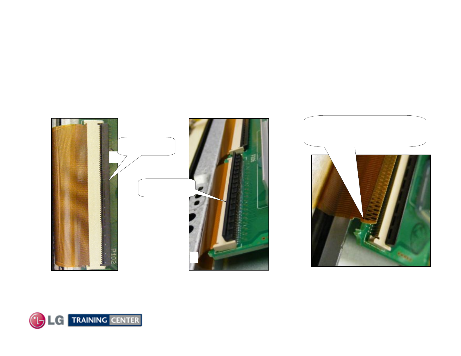
To remove the Ribbon Cable from the connector first carefully lift the Locking Tab from
the back and tilt it forward ( lift from under the tab as shown in Fig 1).
The locking tab must be standing straight up as shown in Fig 2.
Lift up the entire Ribbon Cable gently to release the Tabs on each end. (See Fig 3)
Gently slide the Ribbon Cable free from the connector.
Be sure ribbon tab is released
By lifting the ribbon up slightly,
Gently Pry
Up Here
Locking tab in
upright position
cess is the same.
cess is the same.
before removing ribbon.
Fig 1
To reinstall the Ribbon Cable, carefully slide it back into the slot see ( Fig 3 ), be sure the Tab is seated
securely and press the Locking Tab back to the locked position see ( Fig 2 then Fig 1).
Fig 2
73
July 2010 50PJ350 Plasma
Fig 3
Page 74
Incorrectly Seated Y--
Incorrectly Seated Y
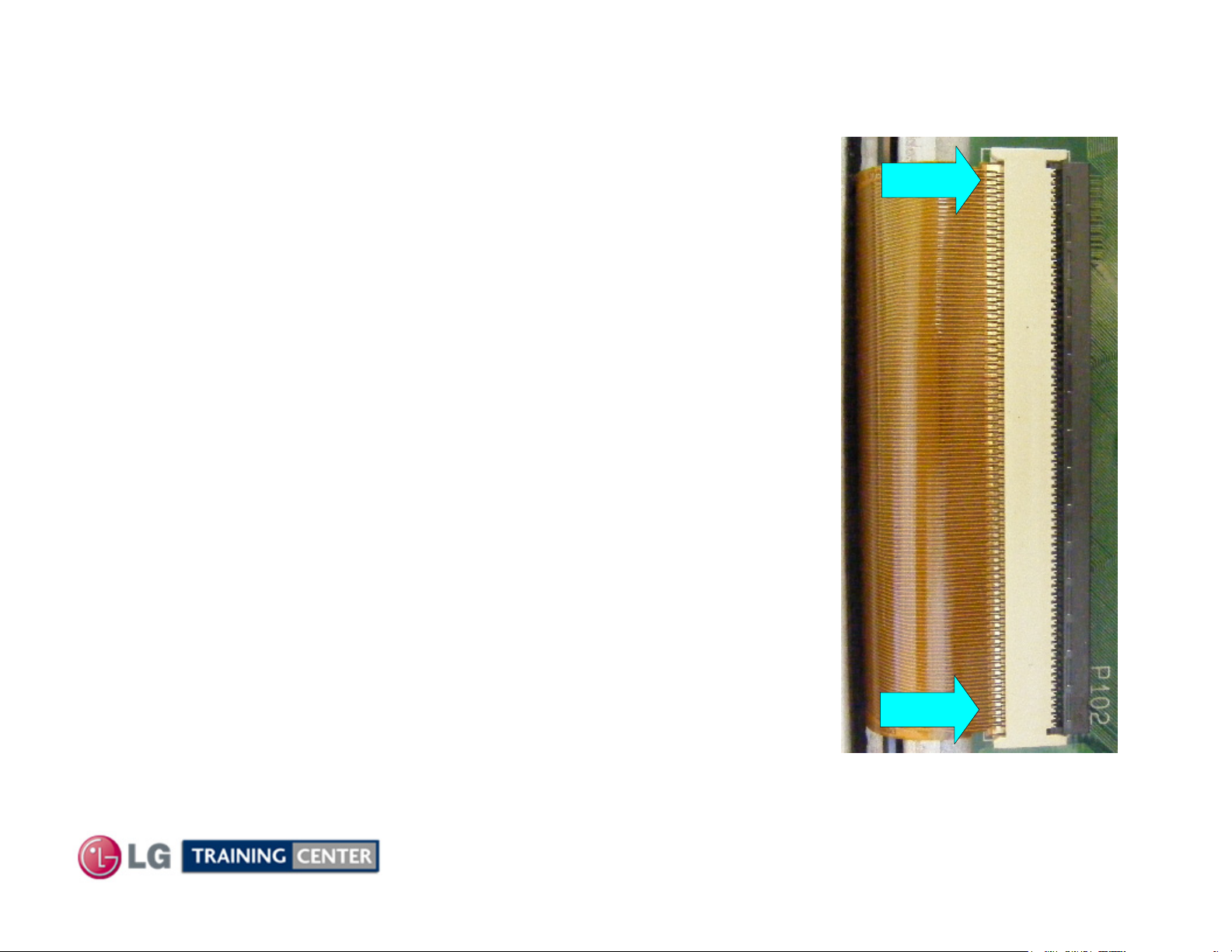
The Ribbon Cable is clearly improperly seated
into the connector. You can tell by observing the
line of the connector compared to the FPC, they
should be parallel.
The Locking Tab will offer a greater resistance to
closing in the case.
Note the cable is crooked. In this case the Tab on
the Ribbon cable was improperly seated at the
Drive Flexible Ribbon Cables
Drive Flexible Ribbon Cables
top. This can cause bars, lines, intermittent lines
abnormalities in the picture.
Remove the ribbon cable and re-seat it correctly.
74
July 2010 50PJ350 Plasma
Page 75
SUS SECTION
ZZ--SUS SECTION
This Section of the Presentation will cover troubleshooting the Z-SUS Board Assembly.
Upon completion of this section the Technician will have a better understanding of the circuit and be
able to locate voltage and diode mode test points needed for troubleshooting and all alignments.
Note: The Z-SUS can not be run “Stand-Alone” in the 50T1 Panel Models.
Locations
Locations
• DC Voltage and Waveform Test Points
• Z BIAS Alignment
• Diode Mode Test Points
Operating Voltages
Power Supply Supplied VS
Y-SUS Supplied 16V Routed through Control Board
Developed on Z-SUS Z Bias
M5V Routed through Control Board
75
July 2010 50PJ350 Plasma
Page 76
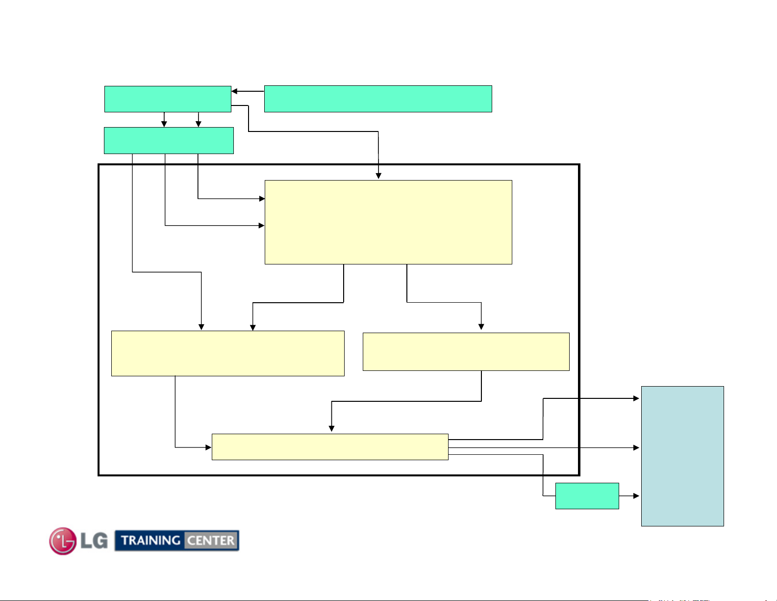
SUS Block Diagram
ZZ--SUS Block Diagram
M5V and VS
Y-SUS Board
16V
M5V
Control Board
M5V
16V
Receives
Logic
Signals
Circuits generate erase,
sustain waveforms
Power Supply Board
VS
Z-SUS board receives VS and
M5V SMPS and 17V from the
Control board
Generates Z Bias 100V
Via 3 FPC
Flexible
Printed
Circuits
NO IPMs
FET Makes Drive waveform
Simplified Block Diagram of Z-SUS (Sustain) Board
76
July 2010 50PJ350 Plasma
Z-SUB
PDP
Display
Panel
Page 77
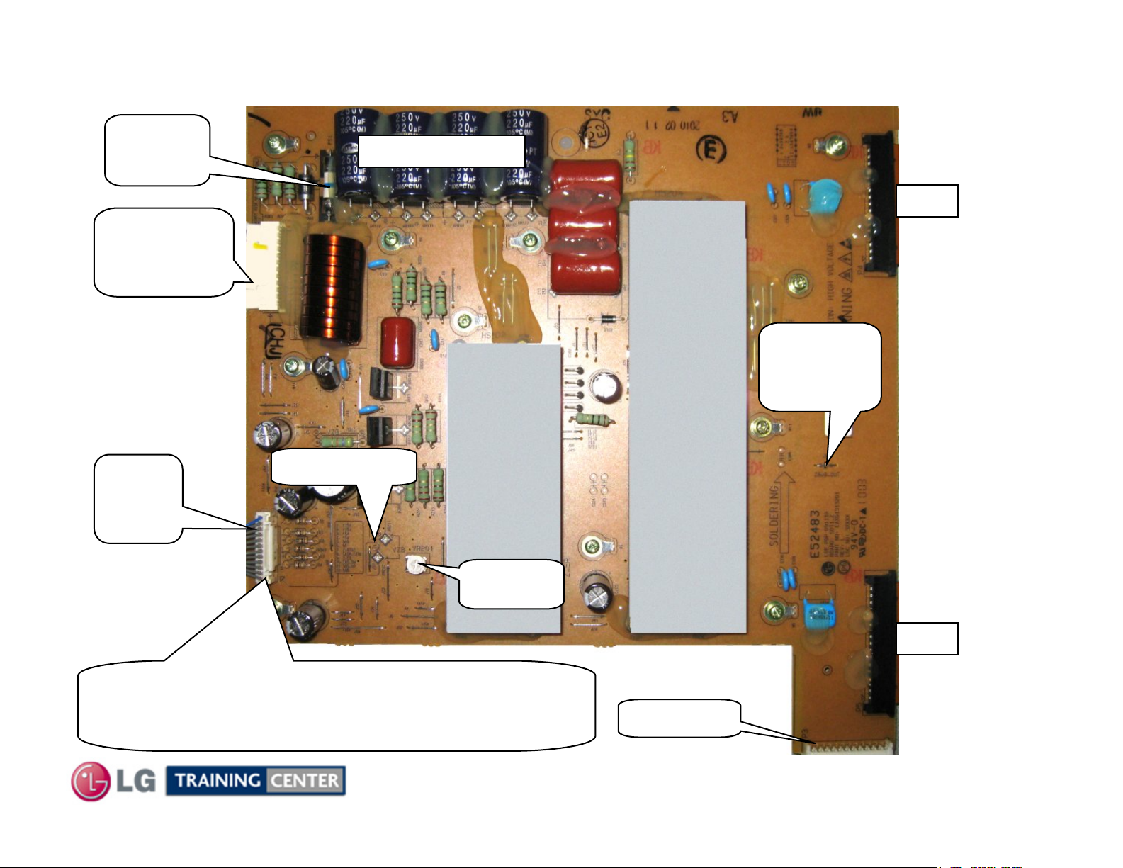
SUS Board Component Identification
ZZ--SUS Board Component Identification
FS1
VS
6.3A/250V
P2
VS from Y-SUS.
Error Com to
the Y-SUS
P/N EBR63040301
P101
No IPMs
No IPMs
P12
Z-Bias TPs
from
Control
M5V from SMPS to the Y-SUS generates +16V.
M5V and 16V are routed through the Control board.
Logic Signals generated on the Control board.
Z-SUS
Waveform
Development
FETs
Z-Bias
VR201
Z-SUS
Output
FETs
No IPMs
P3 To Z-SUB
Z-SUS
Waveform
Test Point
J36
P102
77
July 2010 50PJ350 Plasma
Page 78
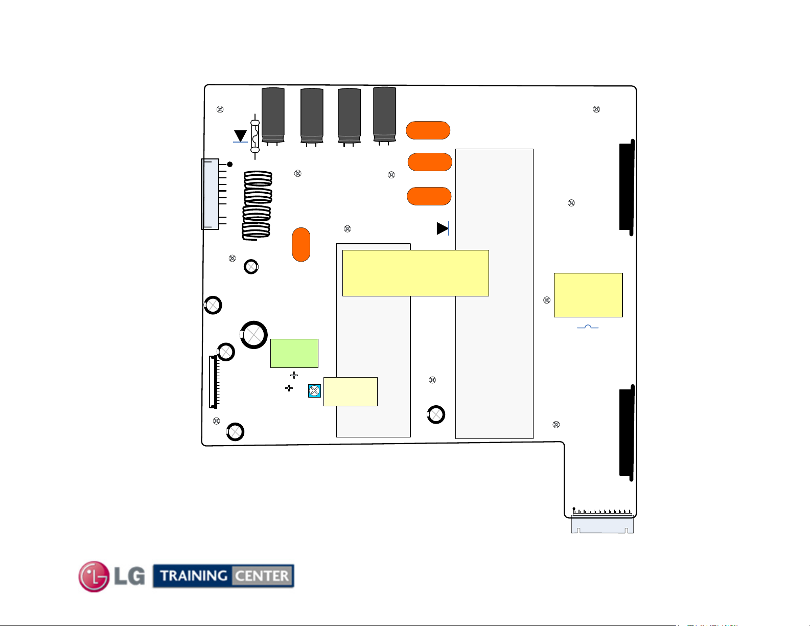
50PJ350 Z-SUS Layout Drawing
50PJ350 Z-SUS Layout Drawing
FS1
VS
D309
4A /
250V
P2
VZB
TP
D312
Z-SUS BOARD
p/n: EBR63040301
P4
Z-Bias
Waveform
J36
P1
VR201
VZB
78
P5
P3
July 2010 50PJ350 Plasma
Page 79
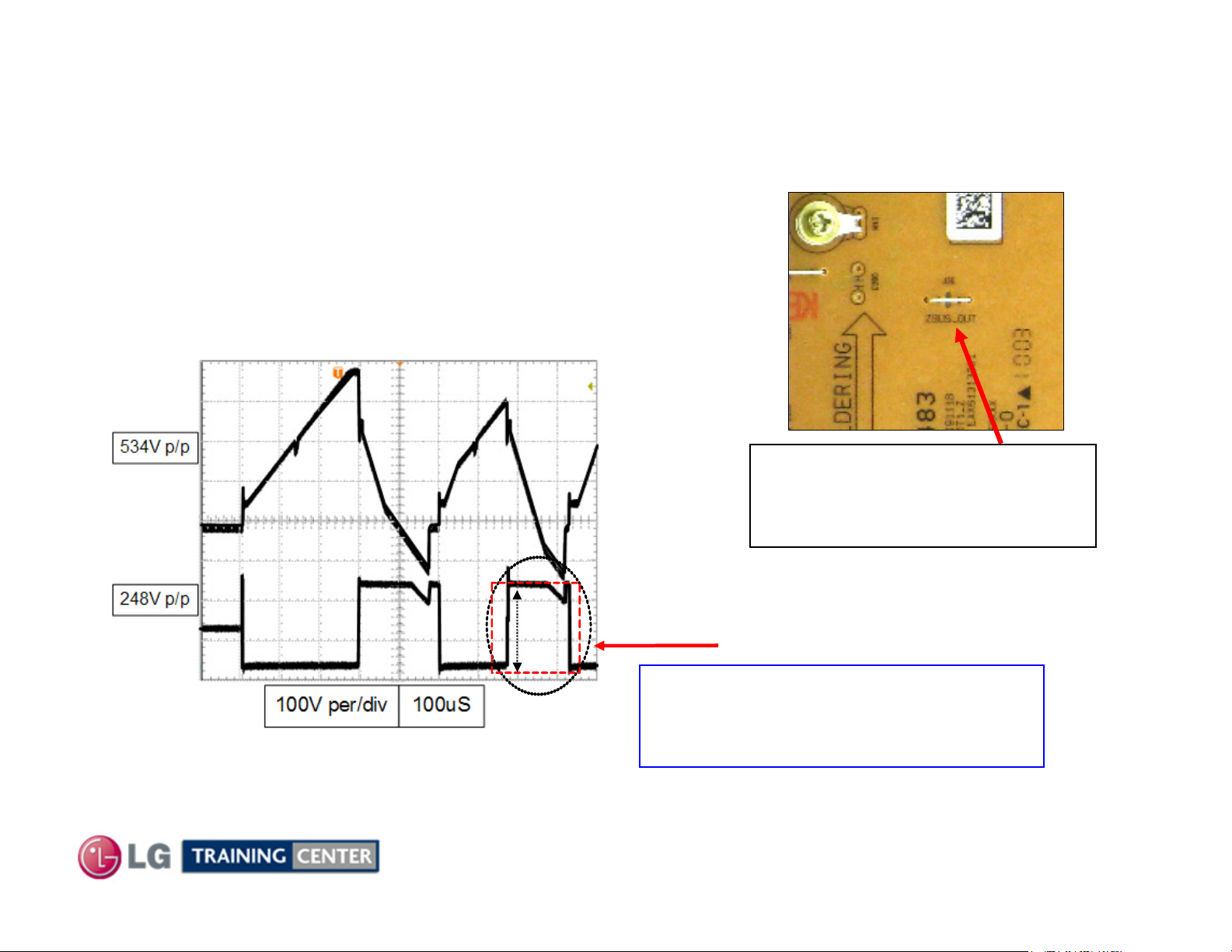
SUS Waveform
ZZ--SUS Waveform
The Z-SUS (in combination with the Y-SUS) generates a
SUSTAIN Signal and an ERASE PULSE for generating
SUSTAIN and DISCHARGE in the Panel.
This waveform is supplied to the panel through two FPC
(Flexible Printed Circuit) connections P101 and P102 and
to the Z-SUB P3 to P7 and then to one FPC (Flexible
Printed Circuit) connections P202.
Reset
Y Drive
Waveform
Z Drive
Waveform
TIP: The Z-Bias (VZB) Adjustment is a
This Waveform is just for reference to observe the effects of Zbz adjustment
(Vzb) Z Bias VR201 manipulates the
offset of this waveform segment.
Vzb voltage 95V ± 1V
This is only to show the effects
of Z-Bias on the waveform.
79
Oscilloscope Connection Point.
J36 to check Z Output waveform.
DC level adjustment.
July 2010 50PJ350 Plasma
Right Hand Side Center.
Page 80
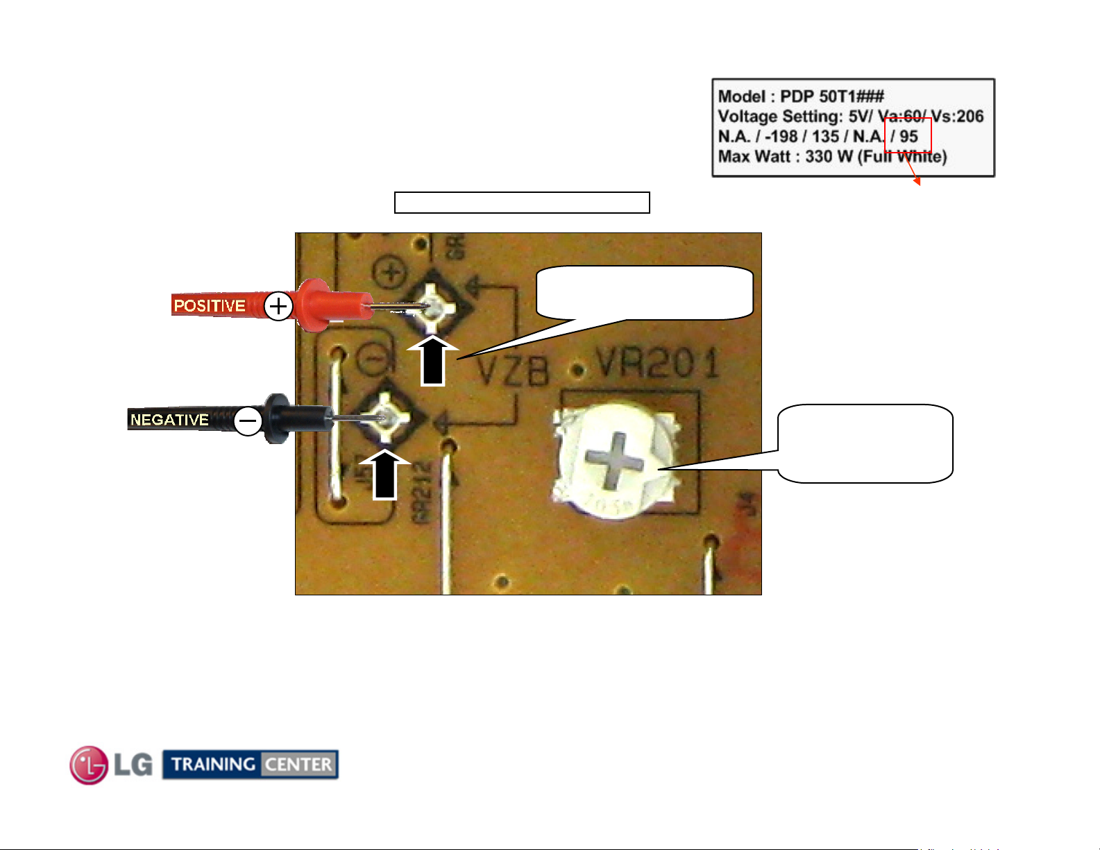
VZB (Z--
VZB (Z
Bias) VR201 Adjustment
Bias) VR201 Adjustment
Read the Voltage Label on the back top center
of the panel when adjusting VR201.
Bottom Left of Z-SUS Board
VZB (Z-Bias) TP
+
-
VZB (Z Bias)
VZB (Z Bias)
VR201
Set should run for 15 minutes, this is the “Heat Run” mode.
Set screen to “White Wash” mode or 100 IRE White input.
All SMPS adjustments should have been completed.
1. Place DC Volt meter between VZB TPs.
2. Adjust VZB (Z Bias) VR201 in accordance with your Panel’s voltage label.
80
July 2010 50PJ350 Plasma
Page 81
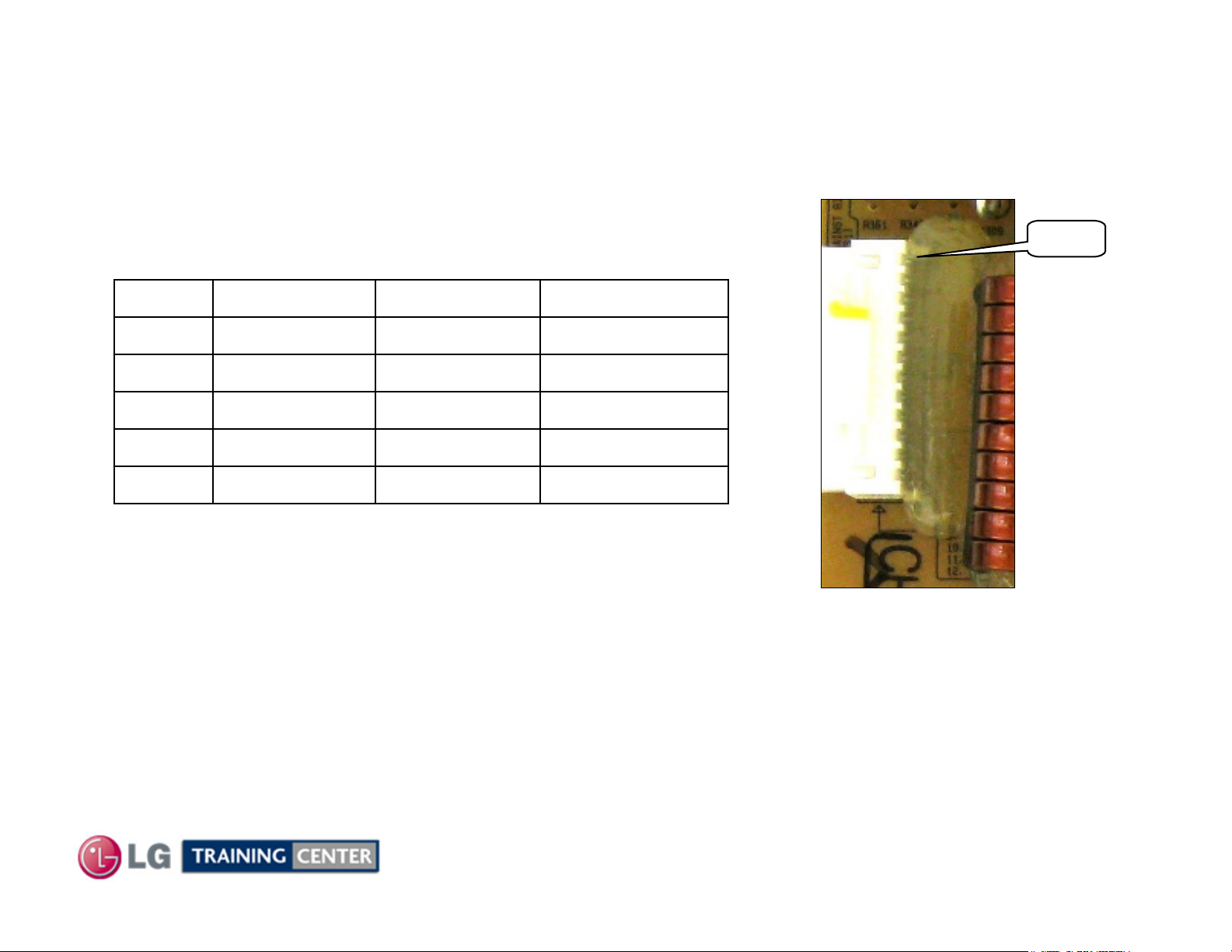
Connector P2 to Y--
Connector P2 to Y
Voltage and Diode Mode Measurements
There are no Stand-By voltages on this connector
P2 "Z-SUS" to "Y-SUS" P211
SUS P211 Voltages and Diode Checks
SUS P211 Voltages and Diode Checks
P2 Location: Top Left
Pin 1
Diode CheckRun LabelPin
GndGndGnd1~2
n/cn/cn/c3
Open*206V+Vs4~5
n/cn/cn/c6
Open98V~102VER_COM7~11
* Note: This voltage will vary in accordance with Panel Label
Diode Mode Readings taken with all connectors Disconnected. DVM in Diode Mode.
81
July 2010 50PJ350 Plasma
Page 82
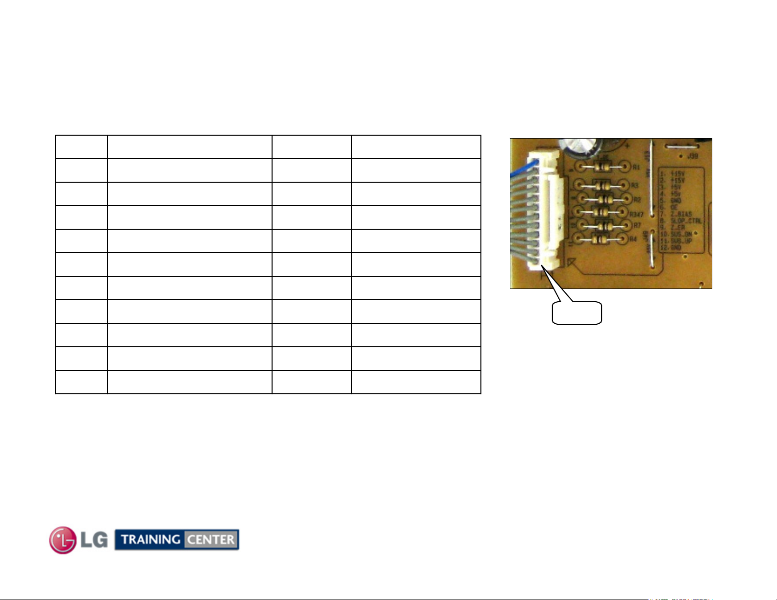
Connector P1 to Control P102 Voltages and Diode Checks
Connector P1 to Control P102 Voltages and Diode Checks
Voltage and Diode Mode Measurements
P1 "Z-SUS Board" to "Control" P101
Diode CheckRun LabelPin
Open16V(+15V)1~2
1.52V4.9V(+5V)3~4
GndGndGnd5
3.09V0.058VY_OE6
Open1.83VZBIAS7
OpenGndSLOP_CONTROL8
P1 Location:
Bottom Left hand side
Open0.14VZ_ER9
Open0.77VZSUS_DN10
Open0.17VZSUS_UP11
GndGndGnd12
There are no Stand-By voltages on this connector
Diode Mode Readings taken with all connectors Disconnected. DVM in Diode Mode.
82
July 2010 50PJ350 Plasma
Pin 1
Page 83
CONTROL BOARD SECTION
CONTROL BOARD SECTION
This Section of the Presentation will cover troubleshooting the Control Board Assembly. Upon
completion of this section the Technician will have a better understanding of the circuit and be
able to locate voltage and diode mode test points needed for troubleshooting.
• DC Voltage and Waveform Test Points
• Diode Mode Test Points
Signals
Main Board Supplied Panel Control and LVDS (Video) Signals
Control Board Generated Y-SUS and Z-SUS Drive Signals (Sustain)
Operating Voltages
X Board Drive Signals (RGB Address)
Y-SUS Supplied
Developed on the Control Board
+5V (M5V) Developed on the SMPS
+16V (Routed to the Z-SUS)
(Not used by the Control Board)
+1.8V for internal use
+3.3V for internal use
+3.3V for the X-Boards (TCPs)
83
July 2010 50PJ350 Plasma
Page 84
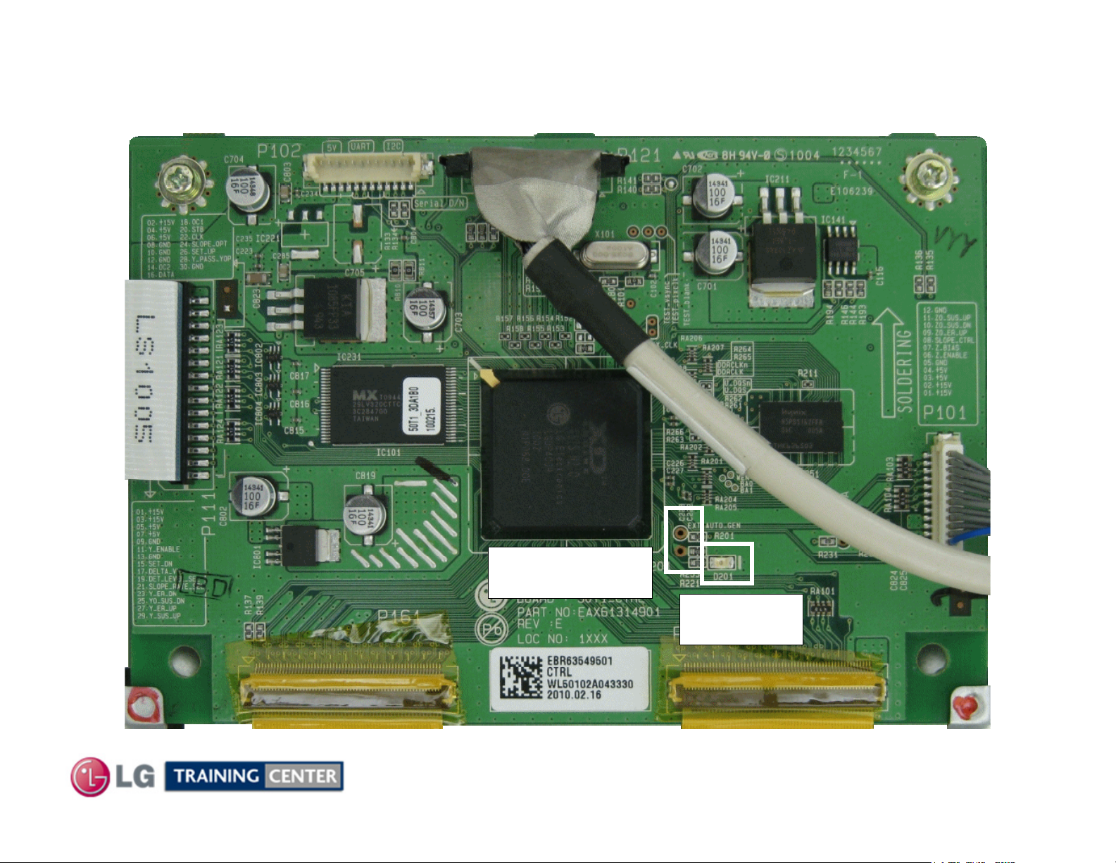
Control Board Pictorial
Control Board Pictorial
n/c (For ROM Updates)
p/n: EBR63549501
P102
P121
P111
IC231
IC801
IC211
P101
Pattern Generator
For Panel Test
D201 Should
be blinking
P161 P162
84
July 2010 50PJ350 Plasma
Page 85
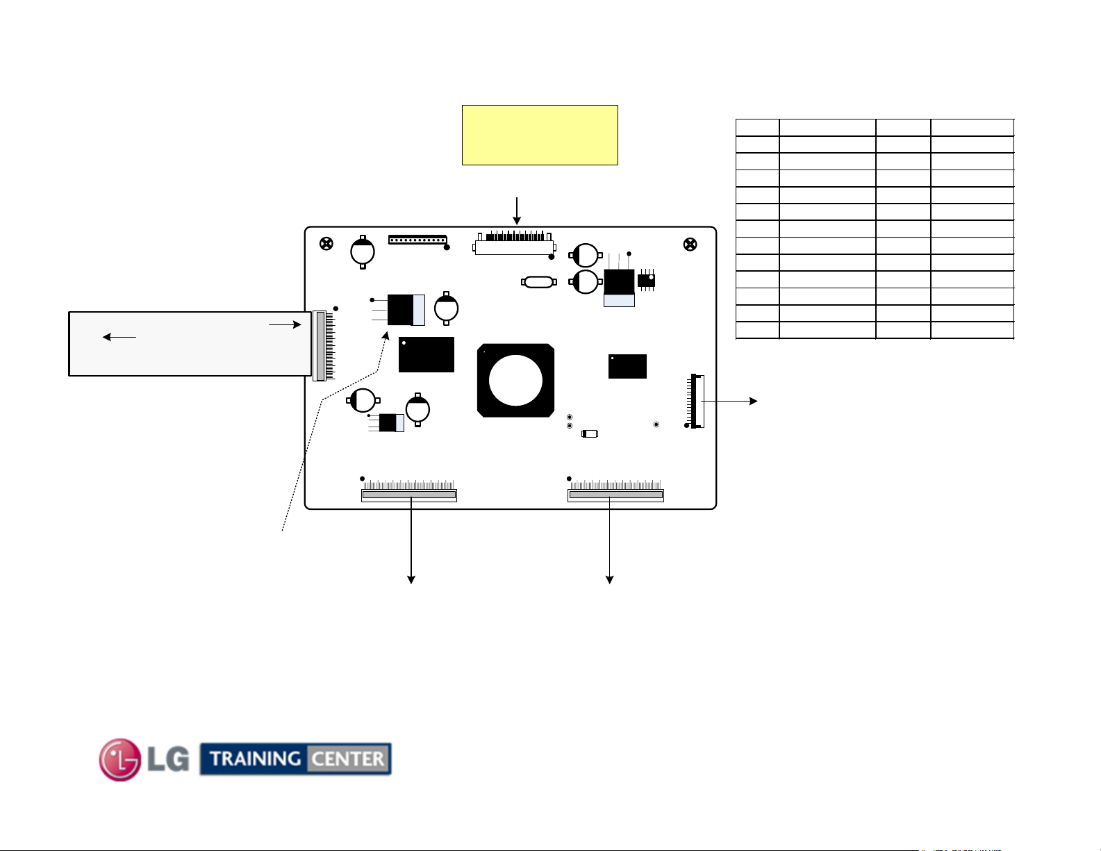
Control Board Component Identification and Checks
Control Board Component Identification and Checks
With the unit on, if D201 is not on, check 5V supply
from FS202 on the Y-SUS.
CONTROL BOARD
p/n: EBR63549501
Pins 4~7 of P111. If present replace the Control
Board. If missing, see (To Test Control Board)
Note: IC231 (3.3V Regulator)
routed to all X Boards
1~3 (16V)
4-7 (M5V)
P102
IC231
LVDS Video
X101
P121
IC141
IC211
Ribbon Cable
Y-SUS and Y Drive Signals
P111
IC101
IC101
IC1
Auto Gen
P101
P101 "Control" to "Z-SUS Board" P1
Pin Label Run Diode
1 (+15V) 16V Open
2 (+15V) 16V Open
3 (+5V) 4.9V 1.52V
4 (+5V) 4.9V 1.52V
5 Gnd Gnd Gnd
6 Y_OE 0.058V 3.09V
7 ZBIAS 1.83V Open
8 Slop_Ctl Gnd Open
9 Z_ER 0.14V Open
10 ZSUS_DN 0.77V Open
11 ZSUS_UP 0.17V Open
12 Gnd Gnd Gnd
Z-Drive Creation Signals
M5V and 16V to Z-SUS
16V protected by
FS204 on Y-SUS
P161
To Test Control Board:
Disconnect all connectors.
Jump STBY 5V from SMPS P813 Pin 13
to pin 3 (bottom leg) of IC231.
Apply AC and turn on the Set. Observe
Control board LED D201, if it’s on, most
likely Control board is OK.
* If the complaint is no video and shorting the points (AutoGen)
causes video to appear suspect the Main board or LVDS cable.
Note: LVDS Cable must be removed for Auto Gen to work.
IC801
X-Drive Center
and Left
RGB Signals
D201 LED
3.3V from IC231
Pins 56~60
85
VS_DA
Remove LVDS Cable. Short across
P162
pattern. When A/C power is applied.
3.3V and X-Drive
Center and Right
RGB Signals
July 2010 50PJ350 Plasma
PANEL TEST: Disconnect P301,
Auto Gen TPs to generate a test
IC231
(1) Gnd
(2) 3.29V
(3) 4.94V
IC801
(1) 1.79V
(2) 3.29V
(3) n/c
(4) 0V
(5) 0V
IC211
(1) Gnd
(2) 1.8V
(3) 3.27V
Page 86
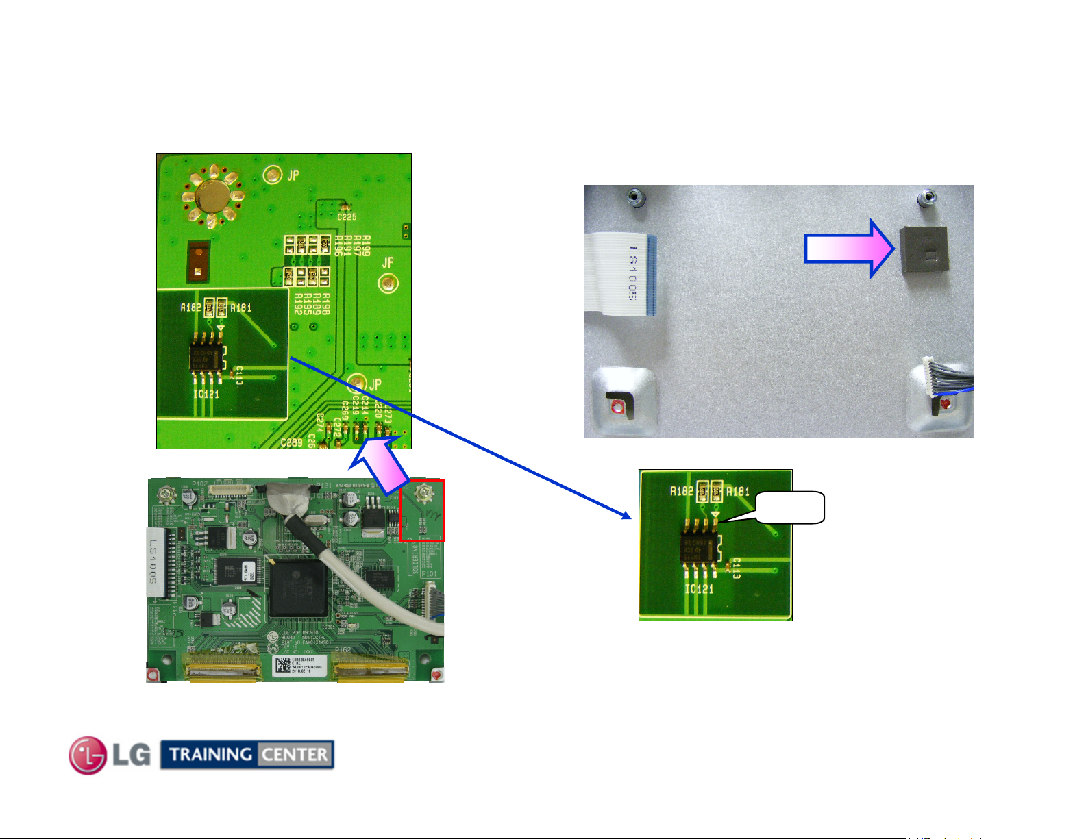
Control Board Temperature Sensor Location (Chocolate)
Control Board Temperature Sensor Location (Chocolate)
BACK SIDE OF
THE BOARD
Be sure the Chocolate
(Heat Transfer Material) remains
in place if the board is removed.
Chocolate
(Heat Transfer Material)
Pin 1
IC121
CONTROL BOARD TEMPERATURE
SENSOR LOCATION
04) 3.3V
05) Gnd
06) 3.3V
Note: The temperature circuit not only protects the panel
from overheating, but it also is responsible for
manipulating the Y-Drive waveform as the panel changes
temperature.
86
July 2010 50PJ350 Plasma
03) Gnd
02) Gnd
01) 3.3V
Page 87
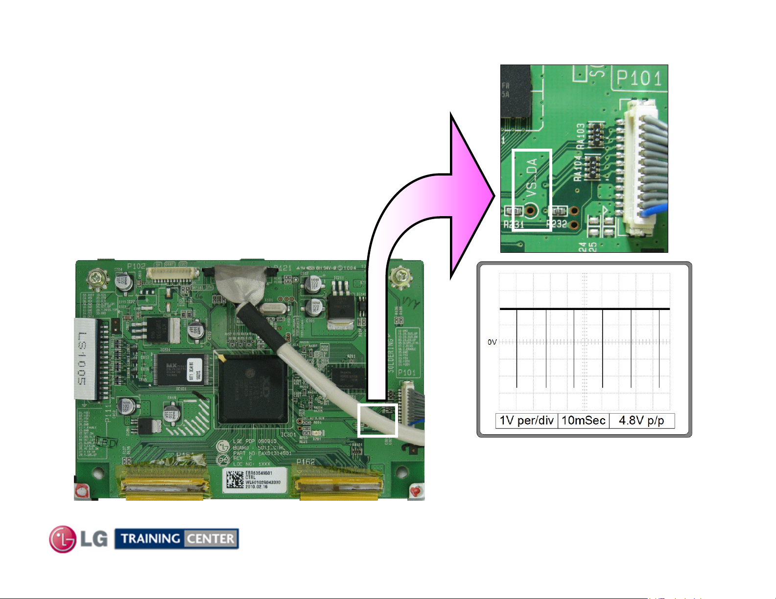
Locking on to the Y--
Locking on to the Y
Note, this TP (VS_DA) can be used as an
External Trigger for scope when locking onto
the Y-Drive (Scan) or the Z-Drive signal.
This signal can also be used
to help lock the scope when observing
the LVDS video signals.
Drive or Z--
Drive or Z
Drive Waveform Tip
Drive Waveform Tip
87
July 2010 50PJ350 Plasma
Page 88
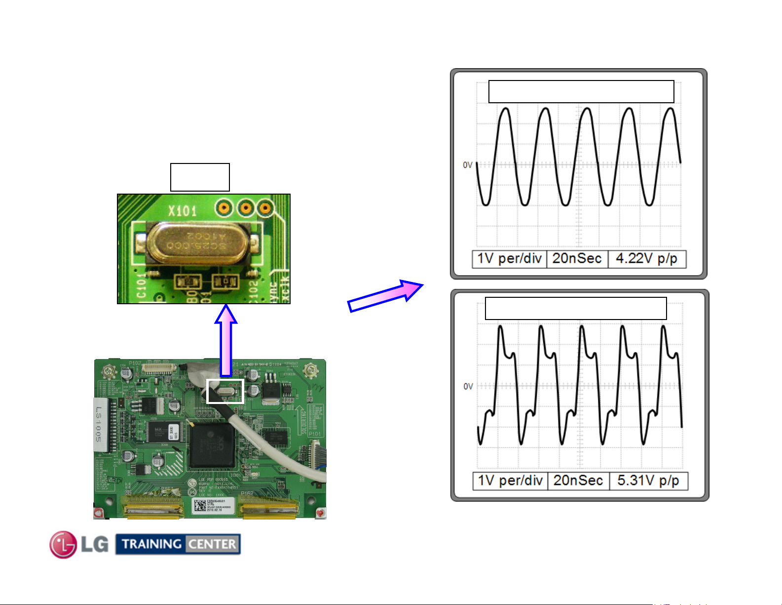
Checking the Crystal X101 ““
Checking the Crystal X101
Clock””
Clock
on the Control Board
on the Control Board
Check the output of the Oscillator (Crystal) X101.
The frequency of the sine wave is 25 MHZ.
Missing this clock signal will halt operation of the panel
drive signals.
X101
Osc. Check: 25Mhz Left Leg
Osc. Check: 25Mhz Right Leg
CONTROL
BOARD
CRYSTAL
LOCATION
88
July 2010 50PJ350 Plasma
Page 89
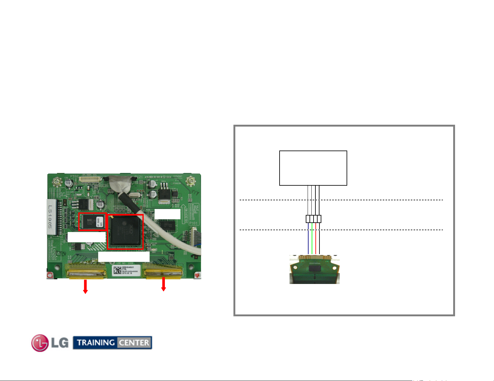
Control Board Signal (Simplified Block Diagram)
Control Board Signal (Simplified Block Diagram)
The Control Board supplies Video Signals to the TCP (Tape Carrier Package) ICs.
If there is a bar defect on the screen, it could be a Control Board problem.
Control Board to X Board
Address Signal Flow
This Picture shows Signal Flow Distribution to help determine the
failure depending on where the it shows on the screen.
DRAM
EEPROM
MCM IC201
To Center
X-Board
To Center
X-Board
Basic Diagram of Control Board
IC201
CONTROL BOARD
MCM
Resistor Array
16 bit words
2 Buffer
Outputs
per TCP
128 Lines per Buffer
256 Lines output Total
X-DRIVE BOARD
PANEL
There are 16 total TCPs.
4096 Vertical Electrodes
4986 (RGB) / 3 =
1365 Total Pixels (H)
89
July 2010 50PJ350 Plasma
Page 90
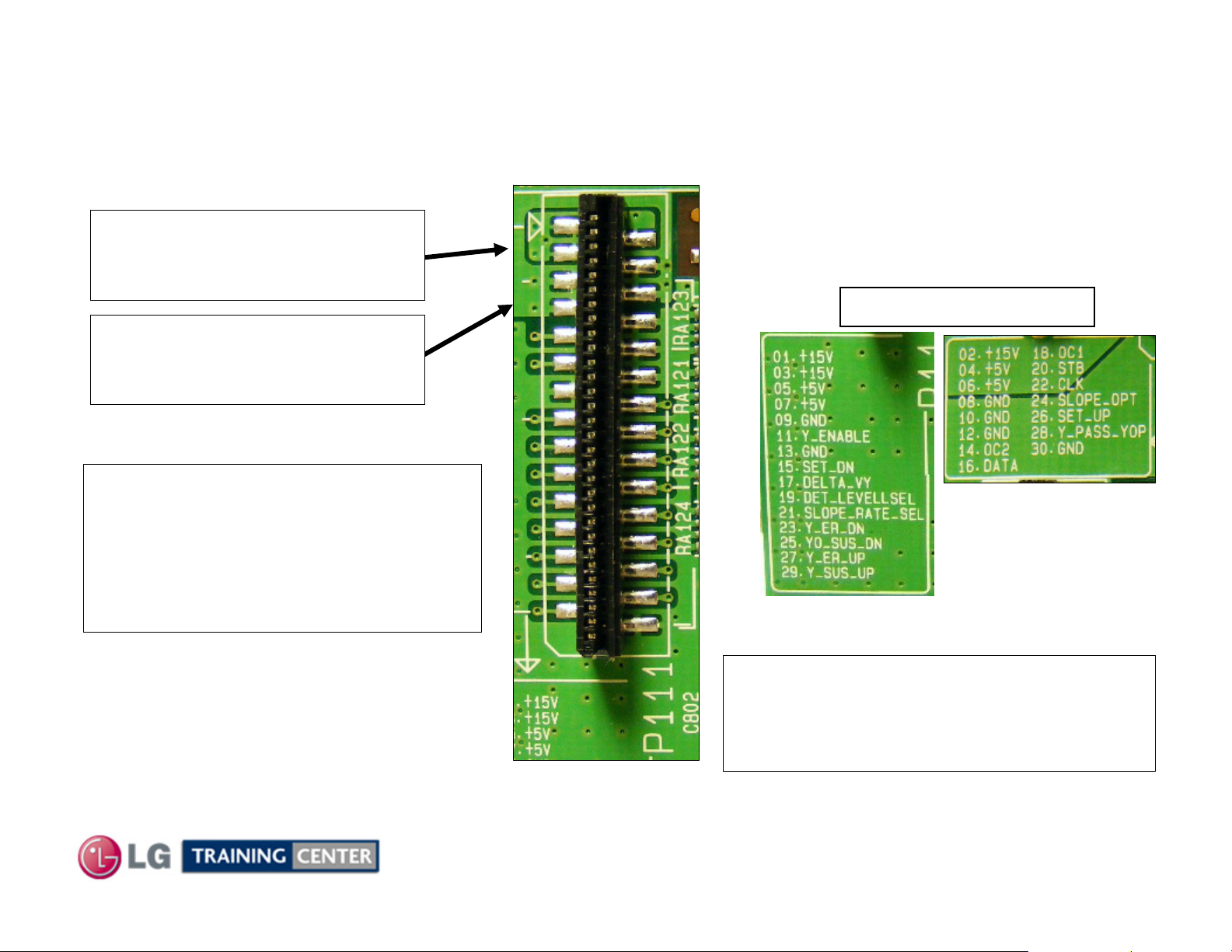
Control Board Connector P111 to Y--
Control Board Connector P111 to Y
These pins are very close together. Use Caution when taking Voltage measurements.
SUS P101 Voltages and Diode Mode Checks
SUS P101 Voltages and Diode Mode Checks
Pins 1 through 3
Receive 16V from the Y-SUS.
Protected on Y-SUS by FS204
Pins 4 through 7
Receive M5V from the Y-SUS.
Protected on Y-SUS by FS202
All the rest are delivering
Y-SUS Waveform development and
Y-Drive logic signals to the Y-SUS
Board (Y-Drive logic signals are simply
routed right through the Y-SUS to the
Y-Drive boards).
Pin c
P111 Label Silk Screen
Note: The +16V is not used by the Control
board, it is routed to the Z-SUS leaving on
P101 Pins 1~2.
The M5V also leaves on P101 Pins 3~4.
90
July 2010 50PJ350 Plasma
Page 91
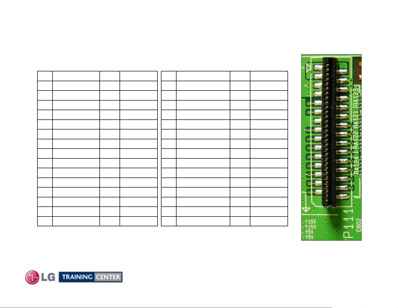
Control P111 to Y--
Control P111 to Y
SUS P101 Plug Information
SUS P101 Plug Information
Note: There are no voltages in Stand-By mode
P111 "Control" Odd Pins to P101 "Y-SUS"
Diode CheckRunLabelPin
Open16V+15V1
Open16V+15V3
1.52V4.9V+5V5
1.52V4.9V+5V7
2.98V0VCTRL_OE9
1.64V0VOE11
GndGndGnd13
2.81V2.08VI_Delta_VY_Det15
2.81V2.09VI_SET_ON17
2.81V0.03VI_Det_Level_Sel19
2.81V1.34VI_Slope_Rate_Sel21
2.81V0VI_YER_DN23
2.82V0.95VI_YSUS_DN_IN25
2.83V0.62VI_YER_UP27
P111 "Control" Even Pins to P101 "Y-SUS"
Diode CheckRunLabelPin
Open16V+15V2
1.4V4.9V+5V4
1.4V4.9V+5V6
GndGndGnd8
GndGndGnd10
GndGndGnd12
2.84V1.78VI_OC214
2.84V0VI_DATA16
2.84V1.43VI_OC118
2.84V1.97VI_STB20
2.82V0.59VI_CLK22
2.82V0.24VI_SET_UP24
2.82V1.01VI_Ramp_Slope_Opt126
2.82V1.08VI_Pass_Top28
2.84V0.06VI_YSUS_UP_IN29
GndGndGnd30
Diode Mode Readings taken with all connectors Disconnected. Black lead on Gnd. DVM in Diode Mode.
91
July 2010 50PJ350 Plasma
Page 92
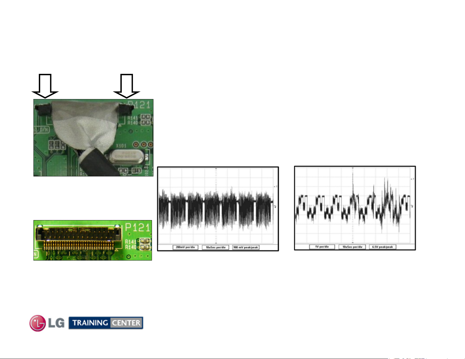
Control Board LVDS P121 Signals
Control Board LVDS P121 Signals
LVDS Cable P121 on Control board shown.
Press two outside tabs inward to release.
Video Signals from the Main Board to the Control Board are referred
to as Low Voltage Differential Signals or LVDS. The video is
delivered in 12 bit LVDS format. Their presence can be confirmed
with the Oscilloscope by monitoring the LVDS signals with SMPTE
P121
LVDS
Color Bar input. Loss of these Signals would confirm the failure is on
the Main Board or the LVDS Cable itself.
LVDS
Example of LVDS Video Signal
LVDS Removed
Pins are close together.
Example of Normal Signals measured at 1V p/p at 10µSec
Pins 2~5, 7~8, 11~12, 15~16, 24~25 are LVDS Video Signals.
Pins 9~10 and 22~23 are clock signals for the data.
92
July 2010 50PJ350 Plasma
Page 93
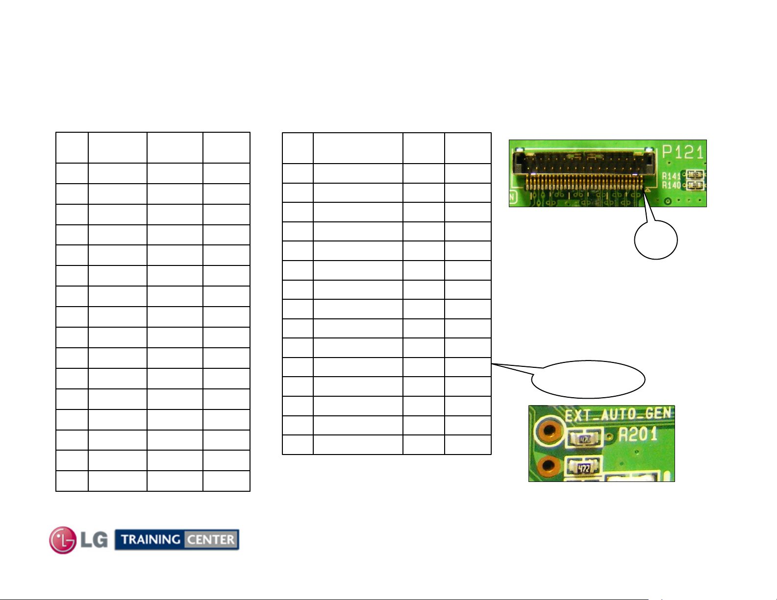
Control Board LVDS P121 Connector Voltages and Diode Check
Control Board LVDS P121 Connector Voltages and Diode Check
P121 Connector "Control Board” to “Main “P703”
P121 LVDS "Control" to P703 "Main"
RunLabelPin
Diode
Check
GndGndGnd1
1.32V1.13VRA2-2
1.36V1.35VRA2+3
1.36V1.21VRB2-4
1.36V1.27VRB2+5
GndGndGnd6
1.32V1.26VRC2-7
1.36V1.22VRC2+8
1.36V1.23VRCLK2-9
1.36V1.23VRCLK2+10
1.36V1.21VRD2-11
1.36V1.26VRD2+12
GndGndGnd13
GndGndGnd14
1.32V1.23VRF2-15
1.36V1.25VRF2+16
P121 LVDS "Control" to P703 "Main"
RunLabelPin
Blue Pins indicate 12 bit
differential video signal
Diode
Check
3.09V3.3VROM_TX17
3.09V3.29VROM_RX18
GndGndGnd19
Openn/cn/c20
Openn/cn/c21
3.08V0.59VPC_SER_CLK22
3.09V3.3VPC_SER_DATA23
1.36V1.23VRE2-24
1.36V1.25VRE2+25
GndGndGnd26
Open2.87VDISP_EN27
Open3.3VModule_SDA128
Open3.3VModule_SCL129
Openn/cn/c30
GndGndGnd31
1
1
Pin 27 is the reason the LVDS
cable must be removed to use the
EX_AUTO_GEN shorting pins to
create multiple internal generated
test patterns (Panel Test).
Enables the
Control Board
Note: There are no voltages in Stand-By mode.
93
July 2010 50PJ350 Plasma
Page 94
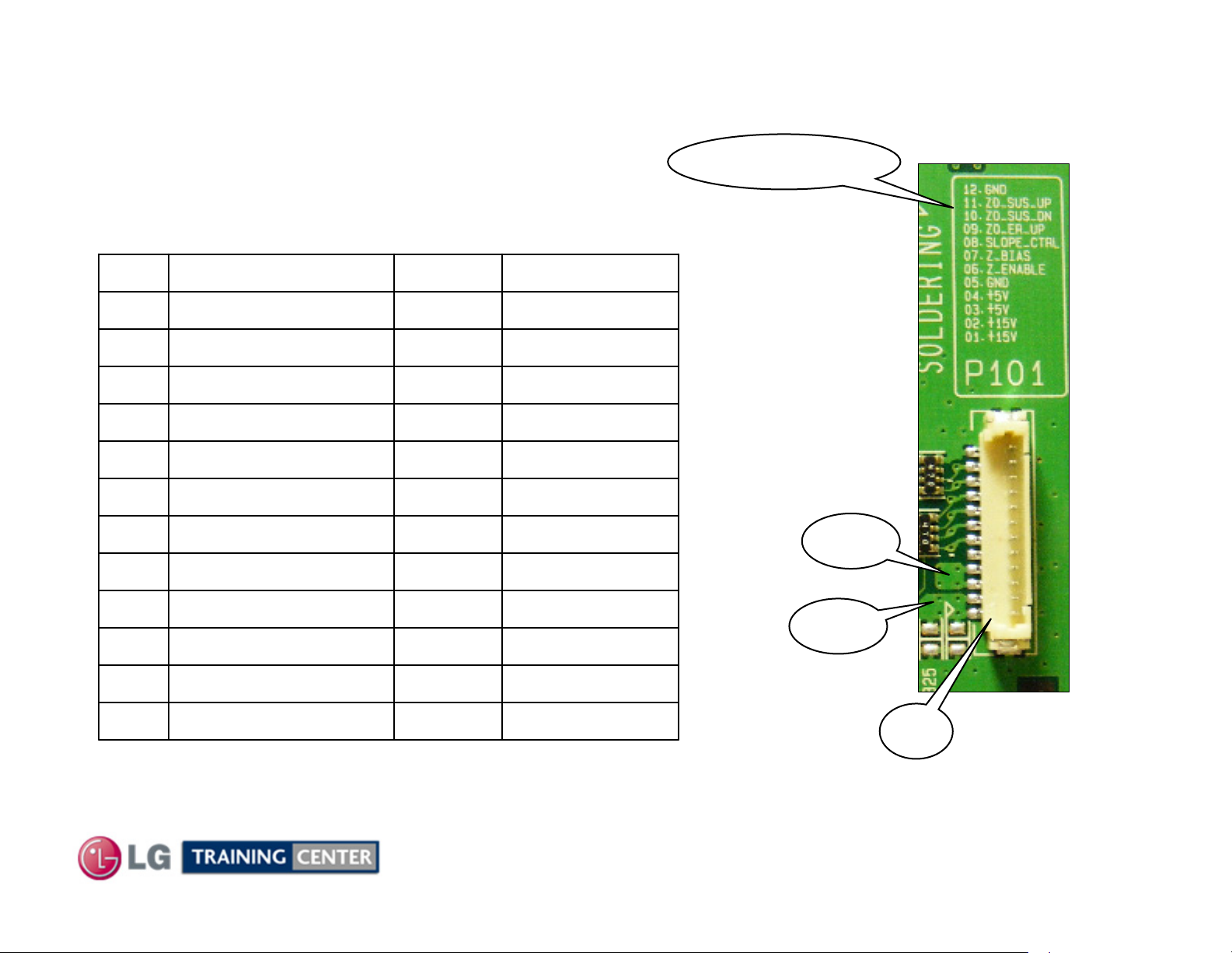
Control Board P101 Connector Pin ID and Voltages
Control Board P101 Connector Pin ID and Voltages
Voltage and Diode Mode Measurements for the Control Board.
Note: There are no voltages in Stand-By mode.
P101 Connector "Control" to "Z-SUS Board" P1
Diode CheckRun LabelPin
Open16V(+15V)1
Open16V(+15V)2
1.52V4.9V(+5V)3
1.52V4.9V(+5V)4
GndGndGnd5
3.09V0.058VY_OE6
P101 Label
P101 Label
Open1.83VZBIAS7
OpenGndSLOP_CONTROL8
Open0.14VZ_ER9
Open0.77VZSUS_DN10
Open0.17VZSUS_UP11
GndGndGnd12
Diode Mode Readings taken with all connectors Disconnected. Black lead on Gnd. DVM in Diode Mode.
94
July 2010 50PJ350 Plasma
5V
5V
16V
16V
1
1
Page 95
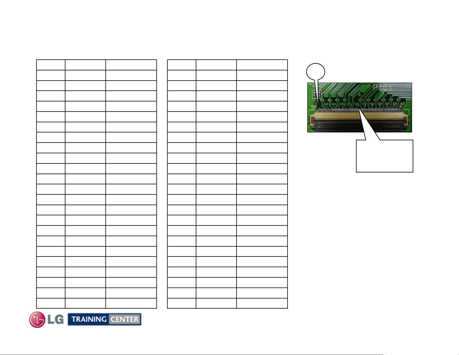
P161 Connector "Control Board””
P161 Connector "Control Board
to ““
to
Center X Board””
Center X Board
P231
P231
P161 Connector to the Center X-Board P231
Diode ModeRun Pin
0.97V1.27V2
0.97V1.0V3
0.97V1.27V6
0.97V1.0V7
0.97V1.27V8
0.97V1.0V9
0.97V1.27V11
0.97V1.0V12
0.97V1.27V14
0.97V1.0V15
0.97V1.27V16
0.97V1.0V17
0.97V1.27V19
0.97V1.0V20
0.97V1.27V21
(Pins not shown are Gnd)
Diode ModeRun Pin
0.97V1.0V33
0.97V1.27V34
0.97V1.0V35
0.97V1.27V37
0.97V1.0V38
0.97V1.27V39
0.97V1.0V40
0.97V1.27V42
0.97V1.0V43
0.97V1.27V44
0.97V1.0V45
0.97V1.27V46
0.97V1.0V47
0.97V1.27V49
0.97V1.0V50
1
1
White hash
White hash
marks count
marks count
as 5
as 5
0.97V1.0V22
0.97V1.27V24
0.97V1.0V25
0.97V1.27V26
0.97V1.0V27
0.97V1.27V29
0.97V1.0V30
0.97V1.27V32
95
0.97V1.27V51
0.97V1.0V52
0.97V1.27V53
1.2V1.87V54
1.2V1.87V56
1.2V3.22V57
1.1V0.49V58
1.1V0.49V59
July 2010 50PJ350 Plasma
Page 96
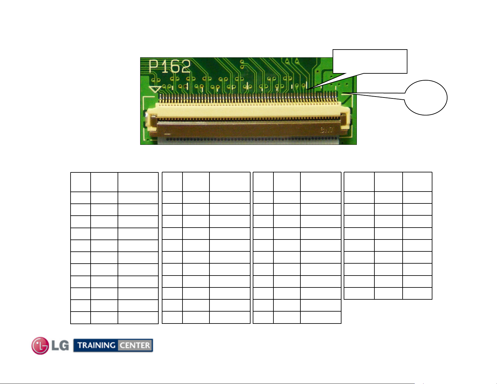
P162 Connector "Control Board””
P162 Connector "Control Board
to ““
to
Center X Board””
Center X Board
P232
P232
White hash marks
White hash marks
count as 5
count as 5
56~60
56~60
3.3V
3.3V
P162 Connector to the Center X-Board P232
Run Pin
Diode
Mode
0.97V1.27V2
0.97V1.0V3
0.97V1.27V4
0.97V1.0V5
0.97V1.27V6
0.97V1.0V7
0.97V1.27V9
0.97V1.0V10
0.97V1.27V11
0.97V1.0V12
0.97V1.27V14
Run Pin
Diode
Mode
0.97V1.27V15
0.97V1.0V17
0.97V1.0V18
0.97V1.27V19
0.97V1.0V20
0.97V1.27V22
0.97V1.0V23
0.97V1.27V24
0.97V1.0V25
0.97V1.27V27
0.97V1.0V28
(Pins not shown are n/c or Gnd)
Run Pin
Diode
Mode
0.97V1.27V29
0.97V1.0V30
0.97V1.27V32
0.97V1.0V33
0.97V1.27V35
0.97V1.0V36
0.97V1.27V37
0.97V1.0V38
0.97V1.27V40
0.97V1.0V41
Run Pin
Note:
0.97V1.27V42
There are no voltages in
Stand-By mode.
Diode
Mode
0.97V1.0V43
0.97V1.27V46
1.2V1.0V47
1.2V1.27V48
1.2V1.0V49
1.1V1.27V50
0.97V1.0V51
0.97V1.27V52
0.67V3.3V56~60
96
July 2010 50PJ350 Plasma
Page 97

X BOARD (LEFT, RIGHT and CENTER) SECTION
X BOARD (LEFT, RIGHT and CENTER) SECTION
The following section gives detailed information about the X boards. These boards
deliver the Color information signal developed on the Control board to the TCPs,
(Taped Carrier Packages). The TCPs are attached to the vertical FPCs, (Flexible
Printed Circuits) which are attached directly to the panel. The X boards are the
attachment points for these FPCs.
These boards have no adjustment.
X-BOARD OPERATIONAL VOLTAGE:
• VA: Originally developed on the Switched Mode Power Supply.
VA (Voltage for Address) is routed through the Y-SUS board, out on P203 pins 5~7
and then to the Left X board via P122 pins 5~7. Va leaves P121 pins 1~5 and is sent
to the Center X-Board via P212 pins 48~50.
It then leaves on P211 pins 1~5 and goes to the Right X P331 pins 48~50.
• 3.3V: Control board develops 3.3V (IC231) and routes to the Center X board via
ribbon connector P232 pins 1~5. It is then distributed to the other X Boards.
To the Left X board via P212 pins 41~42 to P121 pins 11~12.
To the Right X board via P211 pins 11~12 to P331 pins 41~42.
97
July 2010 50PJ350 Plasma
Page 98

X Board Additional Information
X Board Additional Information
There are three X boards, the Left, Center and the Right
(As viewed from the rear of the set).
The three X boards have very little circuitry. They are basically signal
and voltage routing boards.
• They route Va voltage to all of the Taped Carrier Packages (TCPs).
Va is introduced to the Left X board first, then the Left X sends
Va to the Center X and then the Center X sends Va to the Right X.
• They route the Logic (Color) signals from the Control board
to all of the Taped Carrier Packages (TCPs).
• The X boards have connectors to 16 TCPs, 5 on the left and right.
The Center X board has connections to 6 TCPs.
There are a total of 16 TCPs and each TCP has 2 gate arrays, so
there are a total of 32 buffers feeding the panel’s 4986 vertical
electrodes.
98
July 2010 50PJ350 Plasma
Page 99
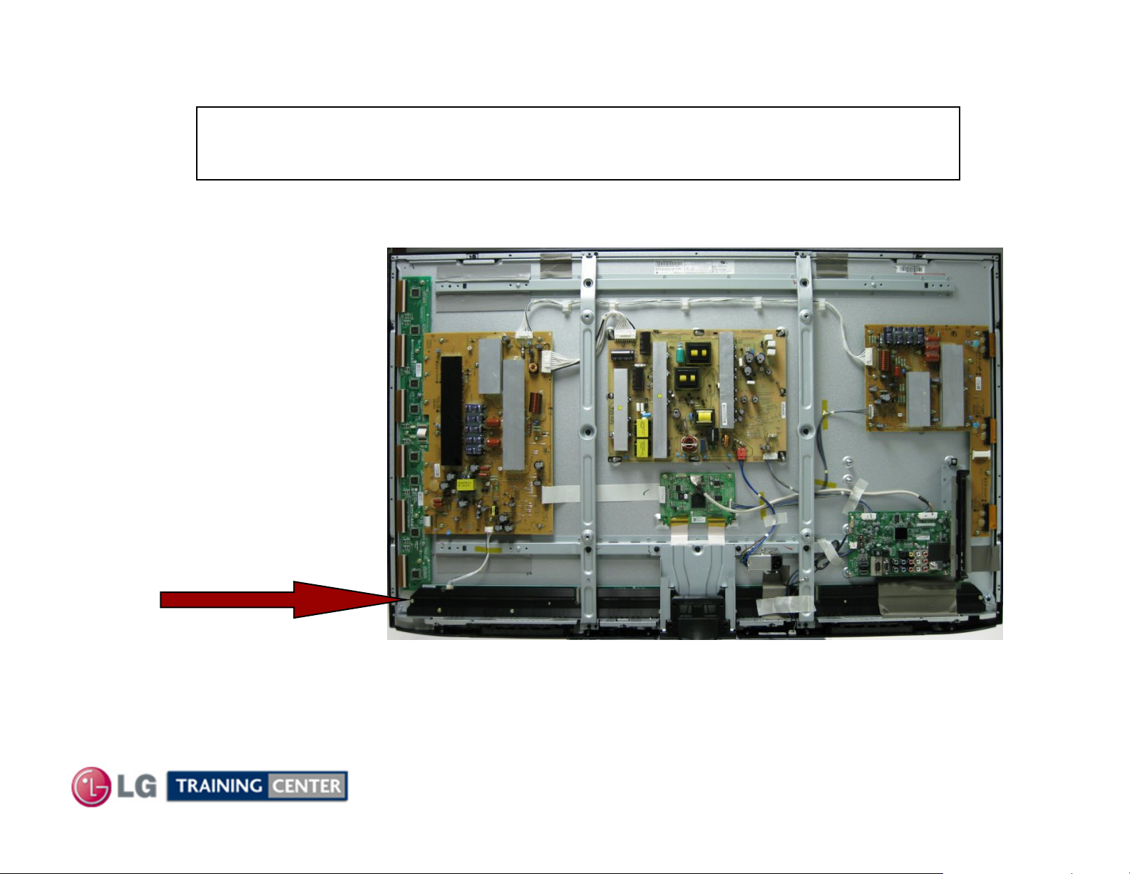
X Board TCP Heat Sink Warning
X Board TCP Heat Sink Warning
NEVER run the television with this heat sink removed.
NEVER run the television with this heat sink removed.
Damage to the TCPs will occur and cause a defective panel.
Damage to the TCPs will occur and cause a defective panel.
The Vertical Address
The Vertical Address
buffers (TCPs) have
buffers (TCPs) have
one heat sink
one heat sink
indicated by the arrow.
indicated by the arrow.
It protects all 16 TCPs.
It protects all 16 TCPs.
99
July 2010 50PJ350 Plasma
Page 100
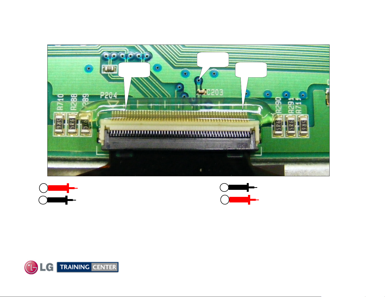
X Board Layout Primary Circuit Diode Check
X Board Layout Primary Circuit Diode Check
The three X-Boards have similar circuit layouts for the connections going to the TCPs, as shown below.
3.3V
VA
Pins 4~7
Pins 32~33
VA
Pins 44~47
Gnd
+
-
On any Va (0.55V) TCPs connected.
On any Va (0.6V) TCPs disconnected.
On 3.3V (0.6V) TCPs connected.
On 3.3V (1.09V) TCPs disconnected.
On Gnd
On the below:
VA source
disconnected
from Left X board
100
-
+
On any Va (Open) TCPs connected.
On any Va (Open) TCPs disconnected.
On 3.3V (1.9V) TCPs connected.
On 3.3V (2.5V) TCPs connected.
On Gnd
On the below:
July 2010 50PJ350 Plasma
 Loading...