


SERVICE MANUAL
Sec. 1: Main Section |
|
Sec. 2: Deck Mechanism Section |
I Specifications |
|
I Standard Maintenance |
I Preparation for Servicing |
|
I Alignment for Mechanism |
I Adjustment Procedures |
|
I Disassembly/Assembly of Mechanism |
I Schematic Diagrams |
|
I Alignment Procedures of Mechanism |
I CBA’s |
|
I Deck Exploded Views |
I Exploded views |
|
I Deck Parts List |
I Parts List |
|
|
|
|
|
DVD PLAYER &
VIDEO CASSETTE RECORDER
DPVR-5505
DPVR-5505V
DPVR-5805
PAL
Downloaded from www.Manualslib.com manuals search engine

MAIN SECTION
DVD PLAYER &
VIDEO CASSETTE RECORDER
DPVR-5505/DPVR-5505V /DPVR-5805
Sec. 1: Main Section
ISpecifications
IPreparation for Servicing
IAdjustment Procedures
ISchematic Diagrams
ICBA’s
IExploded Views
IParts List
TABLE OF CONTENTS
Specifications . . . . . . . . . . . . . . . . . . . . . . . . . . . . . . . . . . . . . . . . . . . . . . . . . . . . . . . . . . . . . . . . . . . . . . . . . 1-1-1 Laser Beam Safety Precautions . . . . . . . . . . . . . . . . . . . . . . . . . . . . . . . . . . . . . . . . . . . . . . . . . . . . . . . . . . . 1-2-1 Important Safety Precautions . . . . . . . . . . . . . . . . . . . . . . . . . . . . . . . . . . . . . . . . . . . . . . . . . . . . . . . . . . . . . 1-3-1 Standard Notes for Servicing . . . . . . . . . . . . . . . . . . . . . . . . . . . . . . . . . . . . . . . . . . . . . . . . . . . . . . . . . . . . . 1-4-1 Preparation for Servicing . . . . . . . . . . . . . . . . . . . . . . . . . . . . . . . . . . . . . . . . . . . . . . . . . . . . . . . . . . . . . . . . 1-5-1 Cabinet Disassembly Instructions. . . . . . . . . . . . . . . . . . . . . . . . . . . . . . . . . . . . . . . . . . . . . . . . . . . . . . . . . . 1-6-1 Electrical Adjustment Instructions. . . . . . . . . . . . . . . . . . . . . . . . . . . . . . . . . . . . . . . . . . . . . . . . . . . . . . . . . . 1-7-1 Firmware Renewal Mode . . . . . . . . . . . . . . . . . . . . . . . . . . . . . . . . . . . . . . . . . . . . . . . . . . . . . . . . . . . . . . . . 1-8-1 Block Diagrams . . . . . . . . . . . . . . . . . . . . . . . . . . . . . . . . . . . . . . . . . . . . . . . . . . . . . . . . . . . . . . . . . . . . . . . . 1-9-1 Function Indicator Symbols. . . . . . . . . . . . . . . . . . . . . . . . . . . . . . . . . . . . . . . . . . . . . . . . . . . . . . . . . . . . . . 1-9-10 Schematic Diagrams / CBA’s and Test Points. . . . . . . . . . . . . . . . . . . . . . . . . . . . . . . . . . . . . . . . . . . . . . . . 1-10-1 Waveforms . . . . . . . . . . . . . . . . . . . . . . . . . . . . . . . . . . . . . . . . . . . . . . . . . . . . . . . . . . . . . . . . . . . . . . . . . . 1-11-1 Wiring Diagram < VCR Section > . . . . . . . . . . . . . . . . . . . . . . . . . . . . . . . . . . . . . . . . . . . . . . . . . . . . . . . . . 1-12-1 Wiring Diagram < DVD Section > . . . . . . . . . . . . . . . . . . . . . . . . . . . . . . . . . . . . . . . . . . . . . . . . . . . . . . . . . 1-12-2 IC Pin Function Descriptions. . . . . . . . . . . . . . . . . . . . . . . . . . . . . . . . . . . . . . . . . . . . . . . . . . . . . . . . . . . . . 1-13-1 Lead Identifications . . . . . . . . . . . . . . . . . . . . . . . . . . . . . . . . . . . . . . . . . . . . . . . . . . . . . . . . . . . . . . . . . . . . 1-14-1 Exploded Views. . . . . . . . . . . . . . . . . . . . . . . . . . . . . . . . . . . . . . . . . . . . . . . . . . . . . . . . . . . . . . . . . . . . . . . 1-15-1 Mechanical Parts List . . . . . . . . . . . . . . . . . . . . . . . . . . . . . . . . . . . . . . . . . . . . . . . . . . . . . . . . . . . . . . . . . . 1-16-1 Electrical Parts List . . . . . . . . . . . . . . . . . . . . . . . . . . . . . . . . . . . . . . . . . . . . . . . . . . . . . . . . . . . . . . . . . . . . 1-17-1
Manufactured under license from Dolby Laboratories. "Dolby" and the double-D symbol are trademarks of Dolby Laboratories.
Downloaded from www.Manualslib.com manuals search engine
SPECIFICATIONS
< VCR Section >
Description |
Unit |
Minimum |
Nominal |
Maximum |
Remark |
|
|
|
|
|
|
|
|
|
|
|
|
1. Video |
|
|
|
|
|
|
|
|
|
|
|
1-1. Video Output (PB) |
Vp-p |
0.8 |
1.0 |
1.2 |
SP Mode |
|
|
|
|
|
|
1-2. Video Output (R/P) |
Vp-p |
0.8 |
1.0 |
1.2 |
|
|
|
|
|
|
|
1-3. Video S/N Y (R/P) |
dB |
40 |
45 |
|
SP Mode, |
|
W/O Burst |
||||
|
|
|
|
|
|
|
|
|
|
|
|
1-4. Video Color S/N AM (R/P) |
dB |
37 |
41 |
|
SP Mode |
|
|
|
|
|
|
1-5. Video Color S/N PM (R/P) |
dB |
30 |
36 |
|
SP Mode |
|
|
|
|
|
|
1-6. Resolution (PB) |
Line |
230 |
245 |
|
SP Mode |
|
|
|
|
|
|
2. Servo |
|
|
|
|
|
|
|
|
|
|
|
2-1. Jitter Low |
sec |
|
0.07 |
0.12 |
SP Mode |
|
|
|
|
|
|
2-2. Wow & Flutter |
% |
|
0.3 |
0.5 |
SP Mode |
|
|
|
|
|
|
3. Normal Audio |
|
|
|
|
|
|
|
|
|
|
|
3-1. Output (PB) |
dBV |
-9 |
-4 |
-3 |
SP Mode |
|
|
|
|
|
|
3-2. Output (R/P) |
dBV |
-9 |
-4 |
-1.5 |
SP Mode |
|
|
|
|
|
|
3-3. S/N (R/P) |
dB |
36 |
41 |
|
SP Mode |
|
|
|
|
|
|
3-4. Distortion (R/P) |
% |
|
1.0 |
4.0 |
SP Mode |
|
|
|
|
|
|
3-5. Freq. resp (R/P) at 200Hz |
dB |
-6 |
-2 |
|
SP Mode |
|
|
|
|
|
|
(-20dB ref. 1kHz) at 8kHz |
dB |
-8 |
-2 |
|
SP Mode |
|
|
|
|
|
|
4. Tuner |
|
|
|
|
|
|
|
|
|
|
|
4-1. Video output |
Vp-p |
0.8 |
1.0 |
1.2 |
E-E Mode |
|
|
|
|
|
|
4-2. Video S/N |
dB |
39 |
44 |
|
E-E Mode |
|
|
|
|
|
|
4-3. Audio output |
dB |
-10 |
-6 |
-2 |
E-E Mode |
|
|
|
|
|
|
4-4. Audio S/N |
dB |
40 |
46 |
|
E-E Mode |
|
|
|
|
|
|
5. Hi-Fi Audio [ DPVR-5805 ] |
|
|
|
|
|
|
|
|
|
|
|
5-1. Output |
dBV |
-12 |
-9 |
-4 |
SP Mode |
|
|
|
|
|
|
5-2. Dynamic Range |
dB |
70 |
85 |
|
SP Mode |
|
|
|
|
|
|
5-3. Freq. resp (6dB B.W) |
Hz |
|
20 ~ 20K |
|
SP Mode |
|
|
|
|
|
|
Note: Nominal specs represent the design specs. All units should be able to approximate these – some will exceed and some may drop slightly below these specs. Limit specs represent the absolute worst condition that still might be considered acceptable; In no case should a unit fail to meet limit specs.
1-1-1 |
H9776SP |
Downloaded from www.Manualslib.com manuals search engine
< DVD Section >
|
|
ITEM |
CONDITIONS |
UNIT |
NOMINAL |
LIMIT |
|
|
|
|
|
|
|
|
|
|
|
|
|
|
1. |
Video Output |
75 ohm load |
Vpp |
1.0 |
± 0.1 |
|
|
|
|
|
|
|
|
2. |
Optical Digital Out |
|
dBm |
-18 |
|
|
|
|
|
|
|
|
|
3. |
Audio (PCM) |
|
|
|
|
|
|
|
|
|
|
|
|
|
3-1. |
Output Level |
1 kHz 0 dB |
Vrms |
2.0 |
|
|
|
|
|
|
|
|
|
3-2. |
S/N |
|
dB |
90 |
|
|
|
|
|
|
|
|
|
3-3. |
Freq. Response |
|
|
|
|
|
|
|
|
|
|
|
|
|
DVD |
fs = 48 kHz ± 0.5dB |
Hz |
20~22 k |
|
|
|
|
|
|
|
|
|
|
CD |
fs = 44.1 kHz ± 0.5dB |
Hz |
20~20 k |
|
|
|
|
|
|
|
|
|
3-4. |
THD+N |
|
|
|
|
|
|
|
|
|
|
|
|
|
DVD |
1 kHz 0dB |
% |
0.01 |
|
|
|
|
|
|
|
|
|
|
CD |
1 kHz 0dB |
% |
0.01 |
|
|
|
|
|
|
|
|
NOTES:
1.All Items are measured without pre-emphasis unless otherwise specified.
2.Power supply : 220 - 240 V ~ 50 Hz
3.Load imp. : 100 k ohm
4.Ambient temperature : 5 °C ~ 40 °C
1-1-2 |
H9776SP |
Downloaded from www.Manualslib.com manuals search engine
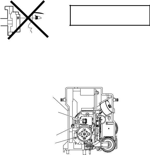
LASER BEAM SAFETY PRECAUTIONS
This DVD player uses a pickup that emits a laser beam.
Do not look directly at the laser beam coming from the pickup or allow it to strike against your skin.
The laser beam is emitted from the location shown in the figure. When checking the laser diode, be sure to keep your eyes at least 30cm away from the pickup lens when the diode is turned on. Do not look directly at the laser beam.
Caution: Use of controls and adjustments, or doing procedures other than those specified herein, may result in hazardous radiation exposure.
Drive Mecha Assembly
Laser Beam Radiation
Laser Pickup
Turntable 
1-2-1 |
E5P_LASER |
Downloaded from www.Manualslib.com manuals search engine
IMPORTANT SAFETY PRECAUTIONS
Product Safety Notice
Some electrical and mechanical parts have special safety-related characteristics which are often not evident from visual inspection, nor can the protection they give necessarily be obtained by replacing them with components rated for higher voltage, wattage, etc. Parts that have special safety characteristics are identified by a ! on schematics and in parts lists. Use of a substitute replacement that does not have the same safety characteristics as the recommended replacement part might create shock, fire, and/or other hazards. The Product’s Safety is under review continuously and new instructions are issued whenever appropriate. Prior to shipment from the factory, our products are carefully inspected to confirm with the recognized product safety and electrical codes of the countries in which they are to be sold. However, in order to maintain such compliance, it is equally important to implement the following precautions when a set is being serviced.
Precautions during Servicing
A.Parts identified by the ! symbol are critical for safety. Replace only with part number specified.
B.In addition to safety, other parts and assemblies are specified for conformance with regulations applying to spurious radiation. These must also be replaced only with specified replacements.
Examples: RF converters, RF cables, noise blocking capacitors, and noise blocking filters, etc.
C.Use specified internal wiring. Note especially:
1)Wires covered with PVC tubing 2)Double insulated wires
3)High voltage leads
D.Use specified insulating materials for hazardous live parts. Note especially:
1)Insulation tape 2)PVC tubing 3)Spacers
4)Insulators for transistors
E.When replacing AC primary side components (transformers, power cord, etc.), wrap ends of wires securely about the terminals before soldering.
F.Observe that the wires do not contact heat producing parts (heatsinks, oxide metal film resistors, fusible resistors, etc.).
G.Check that replaced wires do not contact sharp edges or pointed parts.
H.When a power cord has been replaced, check that 5 - 6 kg of force in any direction will not loosen it.
I.Also check areas surrounding repaired locations.
J.Be careful that foreign objects (screws, solder droplets, etc.) do not remain inside the set.
K.Crimp type wire connector
The power transformer uses crimp type connectors which connect the power cord and the primary side of the transformer. When replacing the transformer, follow these steps carefully and precisely to prevent shock hazards.
Replacement procedure
1)Remove the old connector by cutting the wires at a point close to the connector.
Important: Do not re-use a connector. (Discard it.) 2)Strip about 15 mm of the insulation from the ends of the wires. If the wires are stranded, twist the
strands to avoid frayed conductors.
3)Align the lengths of the wires to be connected. Insert the wires fully into the connector.
4)Use a crimping tool to crimp the metal sleeve at its center. Be sure to crimp fully to the complete closure of the tool.
L.When connecting or disconnecting the internal connectors, first, disconnect the AC plug from the AC outlet.
1-3-1 |
DVD_SFNP |
Downloaded from www.Manualslib.com manuals search engine
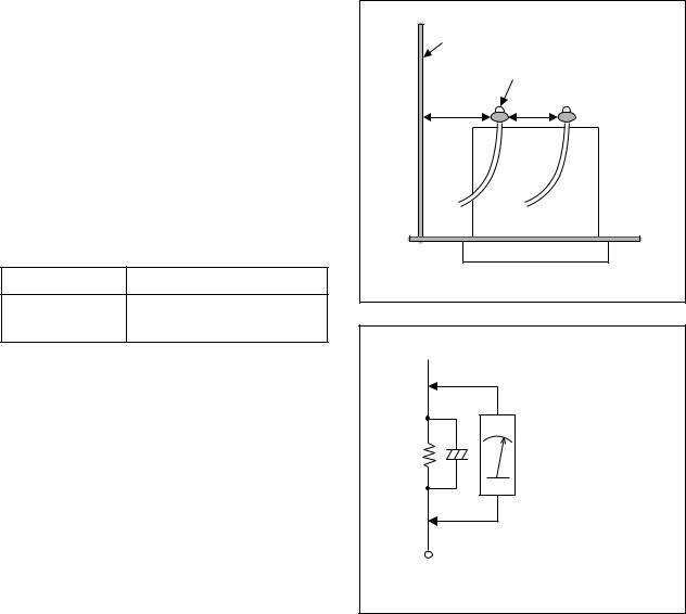
Safety Check after Servicing
Examine the area surrounding the repaired location for damage or deterioration. Observe that screws, parts, and wires have been returned to their original positions. Afterwards, do the following tests and confirm the specified values to verify compliance with safety standards.
1. Clearance Distance
When replacing primary circuit components, confirm specified clearance distance (d) and (d’) between soldered terminals, and between terminals and surrounding metallic parts. (See Fig. 1)
Table 1 : Ratings for selected area
AC Line Voltage |
Clearance Distance (d), (d’) |
≥ 3 mm(d) 220 to 240 V ≥
6 mm(d’)
Note: This table is unofficial and for reference only. Be sure to confirm the precise values.
2. Leakage Current Test
Confirm the specified (or lower) leakage current between B (earth ground, power cord plug prongs) and externally exposed accessible parts (RF terminals, antenna terminals, video and audio input and output terminals, microphone jacks, earphone jacks, etc.) is lower than or equal to the specified value in the table below.
Measuring Method (Power ON) :
Insert load Z between B (earth ground, power cord plug prongs) and exposed accessible parts. Use an AC voltmeter to measure across the terminals of load Z. See Fig. 2 and the following table.
Table 2: Leakage current ratings for selected areas
Chassis or Secondary Conductor |
|
Primary Circuit Terminals |
|
d' |
d |
Fig. 1
 Exposed Accessible Part
Z |
AC Voltmeter |
|
(High Impedance) |
||
|
BOne side of
Power Cord Plug Prongs
Fig. 2
AC Line Voltage |
Load Z |
Leakage Current (i) |
One side of power cord plug |
||
prongs (B) to: |
|||||
|
|
|
|
||
|
|
|
|
|
|
|
|
2kΩ RES. |
i≤0.7mA AC Peak |
RF or |
|
|
|
Connected in |
|||
|
|
i≤2mA DC |
Antenna terminals |
||
|
|
parallel |
|||
220 to 240 V |
|
|
|
||
|
|
|
|
||
|
50kΩ RES. |
i≤0.7mA AC Peak |
|
||
|
|
|
|||
|
|
Connected in |
A/V Input, Output |
||
|
|
i≤2mA DC |
|||
|
|
parallel |
|
||
|
|
|
|
||
|
|
|
|
|
|
Note: This table is unofficial and for reference only. Be sure to confirm the precise values.
1-3-2 |
DVD_SFNP |
Downloaded from www.Manualslib.com manuals search engine
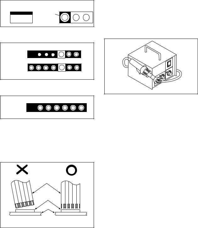
STANDARD NOTES FOR SERVICING
Circuit Board Indications
1.The output pin of the 3 pin Regulator ICs is indicated as shown.
Top View |
Bottom View |
Out |
Input |
In |
2.For other ICs, pin 1 and every fifth pin are indicated as shown.
5
Pin 1 


10
3.The 1st pin of every male connector is indicated as shown.
Pin 1

Instructions for Connectors
1.When you connect or disconnect the FFC (Flexible Foil Connector) cable, be sure to first disconnect the AC cord.
2.FFC (Flexible Foil Connector) cable should be inserted parallel into the connector, not at an angle.
FFC Cable
Connector
CBA
Pb (Lead) Free Solder
When soldering, be sure to use the Pb free solder.
How to Remove / Install Flat Pack-IC
1. Removal
With Hot-Air Flat Pack-IC Desoldering Machine:.
(1)Prepare the hot-air flat pack-IC desoldering machine, then apply hot air to the Flat Pack-IC (about 5 to 6 seconds). (Fig. S-1-1)
Fig. S-1-1
(2)Remove the flat pack-IC with tweezers while applying the hot air.
(3)Bottom of the flat pack-IC is fixed with glue to the CBA; when removing entire flat pack-IC, first apply soldering iron to center of the flat pack-IC and heat up. Then remove (glue will be melted). (Fig. S-1-6)
(4)Release the flat pack-IC from the CBA using tweezers. (Fig. S-1-6)
Caution:
1.The Flat Pack-IC shape may differ by models. Use an appropriate hot-air flat pack-IC desoldering machine, whose shape matches that of the Flat Pack-IC.
2.Do not supply hot air to the chip parts around the flat pack-IC for over 6 seconds because damage to the chip parts may occur. Put masking tape around the flat pack-IC to protect other parts from damage. (Fig. S-1-2)
* Be careful to avoid a short circuit.
1-4-1 |
DVD_NOTE |
Downloaded from www.Manualslib.com manuals search engine
3.The flat pack-IC on the CBA is affixed with glue, so be careful not to break or damage the foil of each pin or the solder lands under the IC when removing it.
|
Hot-air |
|
|
Flat Pack-IC |
|
|
Desoldering |
|
CBA |
Machine |
|
|
||
Masking |
Flat Pack-IC |
|
Tape |
||
|
||
Tweezers |
Fig. S-1-2 |
|
|
With Soldering Iron:
(1)Using desoldering braid, remove the solder from all pins of the flat pack-IC. When you use solder flux which is applied to all pins of the flat pack-IC, you can remove it easily. (Fig. S-1-3)
Flat Pack-IC |
Desoldering Braid |
|
Soldering Iron |
|
Fig. S-1-3 |
(2)Lift each lead of the flat pack-IC upward one by one, using a sharp pin or wire to which solder will not adhere (iron wire). When heating the pins, use a fine tip soldering iron or a hot air desoldering machine. (Fig. S-1-4)
Sharp
 Pin
Pin
Fine Tip
Soldering Iron
Fig. S-1-4
(3)Bottom of the flat pack-IC is fixed with glue to the CBA; when removing entire flat pack-IC, first apply soldering iron to center of the flat pack-IC and heat up. Then remove (glue will be melted). (Fig. S-1-6)
(4)Release the flat pack-IC from the CBA using tweezers. (Fig. S-1-6)
With Iron Wire:
(1)Using desoldering braid, remove the solder from all pins of the flat pack-IC. When you use solder flux which is applied to all pins of the flat pack-IC, you can remove it easily. (Fig. S-1-3)
(2)Affix the wire to a workbench or solid mounting point, as shown in Fig. S-1-5.
(3)While heating the pins using a fine tip soldering iron or hot air blower, pull up the wire as the solder melts so as to lift the IC leads from the CBA contact pads as shown in Fig. S-1-5
1-4-2 |
DVD_NOTE |
Downloaded from www.Manualslib.com manuals search engine
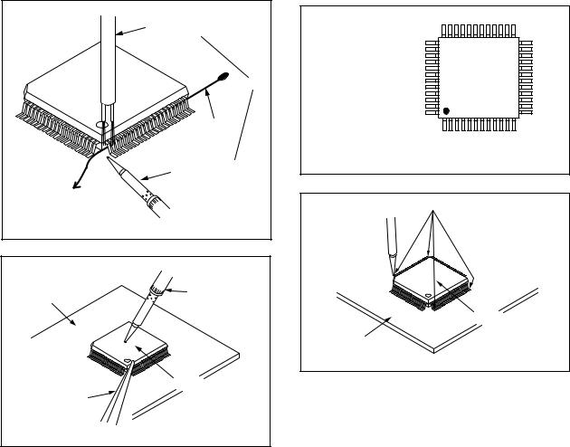
(4)Bottom of the flat pack-IC is fixed with glue to the CBA; when removing entire flat pack-IC, first apply soldering iron to center of the flat pack-IC and heat up. Then remove (glue will be melted). (Fig. S-1-6)
(5)Release the flat pack-IC from the CBA using tweezers. (Fig. S-1-6)
Note:
When using a soldering iron, care must be taken to ensure that the flat pack-IC is not being held by glue. When the flat pack-IC is removed from the CBA, handle it gently because it may be damaged if force is applied.
Hot Air Blower |
or |
Iron Wire |
Soldering Iron |
To Solid |
Mounting Point |
Fig. S-1-5 |
CBA |
Fine Tip |
Soldering Iron |
|
|
Flat Pack-IC |
Tweezers |
|
|
Fig. S-1-6 |
2. Installation
(1)Using desoldering braid, remove the solder from the foil of each pin of the flat pack-IC on the CBA so you can install a replacement flat pack-IC more easily.
(2)The “I” mark on the flat pack-IC indicates pin 1. (See Fig. S-1-7.) Be sure this mark matches the 1 on the PCB when positioning for installation. Then presolder the four corners of the flat pack-IC. (See Fig. S-1-8.)
(3)Solder all pins of the flat pack-IC. Be sure that none of the pins have solder bridges.
Example :
Pin 1 of the Flat Pack-IC
s indicated by a "  " mark.
Fig. S-1-7
Presolder
Flat Pack-IC
CBA
Fig. S-1-8
1-4-3 |
DVD_NOTE |
Downloaded from www.Manualslib.com manuals search engine
Instructions for Handling
Semi-conductors
Electrostatic breakdown of the semi-conductors may occur due to a potential difference caused by electrostatic charge during unpacking or repair work.
1. Ground for Human Body
Be sure to wear a grounding band (1MΩ) that is properly grounded to remove any static electricity that may be charged on the body.
2. Ground for Workbench
(1)Be sure to place a conductive sheet or copper plate with proper grounding (1MΩ) on the workbench or other surface, where the semi-conductors are to be placed. Because the static electricity charge on clothing will not escape through the body grounding band, be careful to avoid contacting semi-con- ductors with your clothing.
< Incorrect > |
CBA |
< Correct > |
Grounding Band
1MΩ
CBA
1MΩ
Conductive Sheet or
Copper Plate
1-4-4 |
DVD_NOTE |
Downloaded from www.Manualslib.com manuals search engine
PREPARATION FOR SERVICING
How to Enter the Service Mode
About Optical Sensors
Caution:
An optical sensor system is used for the Tape Start and End Sensors on this equipment. Carefully read and follow the instructions below. Otherwise the unit may operate erratically.
What to do for preparation
Insert a tape into the Deck Mechanism Assembly and press the PLAY button. The tape will be loaded into the Deck Mechanism Assembly. Make sure the power is on, connect TP501 (S-INH) to GND. This will stop the function of Tape Start Sensor, Tape End Sensor and Reel Sensors. (If these TPs are connected before plugging in the unit, the function of the sensors will stay valid.) See Fig. 1.
Note: Because the Tape End Sensors are inactive, do not run a tape all the way to the start or the end of the tape to avoid tape damage.
Q503 |
Q504 |
TP501 S-INH |
Fig. 1 |
1-5-1 |
H9700PFS |
Downloaded from www.Manualslib.com manuals search engine

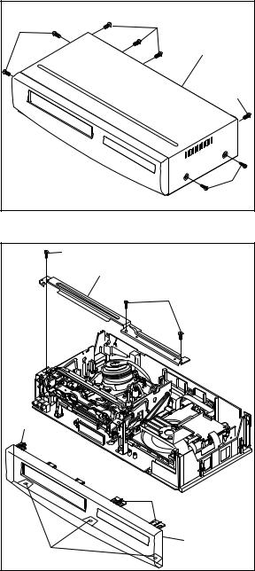
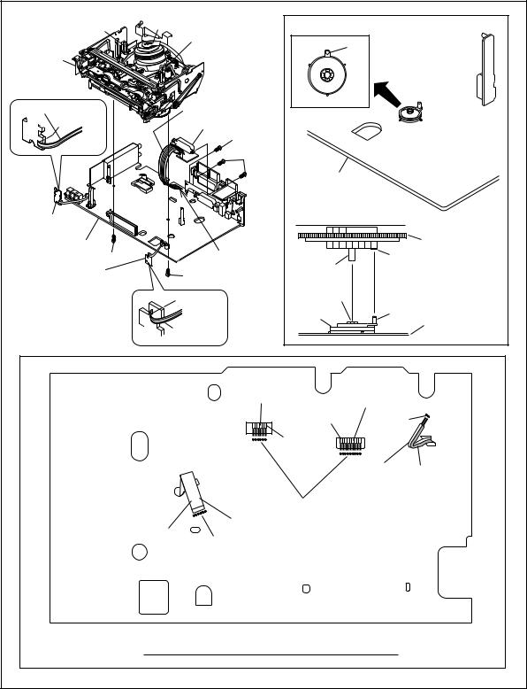
CABINET DISASSEMBLY INSTRUCTIONS
1. Disassembly Flowchart
This flowchart indicates the disassembly steps to gain access to item(s) to be serviced. When reassembling, follow the steps in reverse order. Bend, route, and dress the cables as they were originally.
[1] Top Case
[2]Front Assembly
[3]Top Bracket
[4] DVD Mecha Assembly |
|
|
[8] DVD Main CBA |
|
|
||||
|
|
|
|
|
|
|
|
|
|
[5]Partition Plate
[6]Power Supply CBA
[7]Loader Holder
[9]VCR Chassis Unit
[10]Deck Assembly
[11]DVD Open/Close CBA
[12]Power SW CBA
[13]Main CBA
[14]Jack-A CBA
2.Disassembly Method
ID/ |
|
|
REMOVAL |
|
|
|
|
|
|
||
|
|
REMOVE/*UNHOOK/ |
|
||
LOC. |
PART |
Fig. |
|
||
No. |
|
UNLOCK/RELEASE/ |
Note |
||
|
No. |
||||
|
|
|
UNPLUG/DESOLDER |
|
|
|
|
|
|
|
|
|
|
|
|
|
|
[1] |
Top Case |
D1 |
8(S-1) |
- |
|
|
|
|
|
|
|
|
Front |
|
|
1 |
|
[2] |
D2 |
*3(L-1), *3(L-2) |
1-1 |
||
Assembly |
|||||
|
|
|
1-2 |
||
|
|
|
|
||
|
|
|
|
|
|
[3] |
Top |
D2 |
3(S-2) |
- |
|
Bracket |
|||||
|
|
|
|
||
|
|
|
|
|
|
|
DVD |
|
4(S-3), *CN401, |
|
|
[4] |
Mecha |
D3 |
- |
||
*CN601 |
|||||
|
Assembly |
|
|
||
|
|
|
|
||
|
|
|
|
|
|
[5] |
Partition |
D3 |
(S-4) |
- |
|
Plate |
|||||
|
|
|
|
||
|
|
|
|
|
|
|
Power |
|
|
|
|
[6] |
Suppy |
D3 |
2(S-5), CN501 |
- |
|
|
CBA |
|
|
|
|
|
|
|
|
|
ID/ |
|
|
REMOVAL |
|
|
|
|
|
|
||
|
|
REMOVE/*UNHOOK/ |
|
||
LOC. |
PART |
Fig. |
|
||
No. |
|
UNLOCK/RELEASE/ |
Note |
||
|
|
No. |
UNPLUG/DESOLDER |
|
|
|
|
|
|
|
|
[7] |
Loader |
D3 |
2(S-6) |
- |
|
Holder |
|||||
|
|
|
|
||
|
|
|
|
|
|
|
DVD Main |
|
2(S-7), *CN201, |
2 |
|
[8] |
D4 |
2-1 |
|||
CBA |
*CN301 |
2-2 |
|||
|
|
||||
|
|
|
|
3 |
|
|
|
|
|
|
|
|
VCR |
|
5(S-8), 2(S-9), |
|
|
[9] |
Chassis |
D5 |
- |
||
2(S-10), (L-3) |
|||||
|
Unit |
|
|
||
|
|
|
|
||
|
|
|
|
|
|
[10] |
Deck |
D6 |
Desolder, |
4,5 |
|
Assembly |
2(S-11), (S-12) |
||||
|
|
|
|||
|
|
|
|
|
|
|
DVD |
|
|
|
|
[11] |
Open/ |
D6 |
Desolder |
- |
|
Close |
|||||
|
|
|
|
||
|
CBA |
|
|
|
|
|
|
|
|
|
|
[12] |
Power SW |
D6 |
Desolder |
- |
|
CBA |
|||||
|
|
|
|
||
|
|
|
|
|
|
[13] |
Main CBA |
D6 |
---------- |
- |
|
|
|
|
|
|
|
[14] |
Jack-A |
D6 |
Desolder, 2(S-13) |
- |
|
CBA |
|||||
|
|
|
|
||
|
|
|
|
|
|
↓ |
↓ |
↓ |
↓ |
↓ |
|
(1) |
(2) |
(3) |
(4) |
(5) |
Note:
(1): Identification (location) No. of parts in the figures (2): Name of the part
(3): Figure Number for reference
(4): Identification of parts to be removed, unhooked, unlocked, released, unplugged, unclamped, or desoldered.
P=Spring, L=Locking Tab, S=Screw, CN=Connector
*=Unhook, Unlock, Release, Unplug, or Desolder e.g. 2(S-2) = two Screws (S-2),
2(L-2) = two Locking Tabs (L-2) (5): Refer to “Reference Notes.”
1-6-1 |
H9773DC |
Downloaded from www.Manualslib.com manuals search engine
Reference Notes
CAUTION 1: Locking Tabs (L-1) and (L-2) are fragile. Be careful not to break them.
1-1. Release three Locking Tabs (L-1).
1-2. Release three Locking Tabs (L-2), then remove the Front Assembly.
CAUTION 2: Electrostatic breakdown of the laser diode in the optical system block may occur as a potential difference caused by electrostatic charge accumulated on cloth, human body etc, during unpacking or repair work.
To avoid damage of pickup follow next procedures.
2-1. Disconnect Connector (CN301). Remove two Screws (S-7) and lift the DVD Main CBA Unit. (Fig. D4)
2-2. Short the three short lands of FPC cable with solder before removing the FFC cable (CN201) from it. If you disconnect the FFC cable (CN201), the laser diode of pickup will be destroyed. (Fig. D4)
CAUTION 3: When reassembling, confirm the FFC cable (CN201) is connected completely. Then remove the solder from the three short lands of FPC cable. (Fig. D4)
4.When reassembling, solder wire jumpers as shown in Fig. D6.
5.Before installing the Deck Assembly, be sure to place the pin of LD-SW on Main CBA as shown in Fig. D6. Then, install the Deck Assembly while aligning the hole of Cam Gear with the pin of LDSW, the shaft of Cam Gear with the hole of LD-SW as shown in Fig. D6.
(S-1) |
(S-1) |
|
[1] Top Case |
|
(S-1) |
|
(S-1) |
|
Fig. D1 |
|
(S-2) |
[3] Top Blacket
(S-2)
(L-1)
(L-1)
[2] Front
Assembly
(L-2)
Fig. D2
1-6-2 |
H9773DC |
Downloaded from www.Manualslib.com manuals search engine
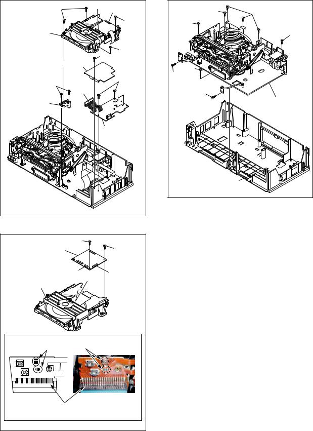
(S-3) |
CN401 |
|
CN601 |
||
|
||
|
(S-3) |
|
[4] DVD Mecha |
|
|
Assembly |
|
|
|
(S-3) |
|
[5] Partition Plate |
(S-4) |
|
|
||
|
(S-5) |
|
(S-6) |
|
|
CN501 |
||
[7] Loader |
|
|
Holder |
|
|
|
[6] Power |
|
|
Supply CBA |
|
|
Fig. D3 |
|
(S-7) |
|
|
[8] DVD Main CBA |
(S-7) |
|
CN301 |
CN201 |
|
A |
||
|
||
DVD Mecha
(S-9) |
(S-8) |
(S-8) |
|
|
(S-9) |
(S-8) |
|
(S-10) |
|
(S-10) |
|
|
[9] VCR Chassis Unit |
|
(L-3) |
|
Fig. D5 |
Short the three short lands by soldering. (Either of two places.)
Connector
View for A
Fig. D4
1-6-3 |
H9773DC |
Downloaded from www.Manualslib.com manuals search engine
|
Cylinder |
|
|
|
|
FE Head |
Assembly |
|
|
|
|
|
ACE Head |
|
|
|
|
|
|
|
Pin |
|
|
[10] Deck |
|
Assembly |
|
|
|
|
|
|
|
|
|
Assembly |
|
|
|
|
|
Lead with blue stripe |
Lead with blue stripe |
|
|
SW507 |
|
|
|
LD-SW |
|||
Desolder |
|
[14] Jack-A CBA |
|
|
|
|
|
|
|
||
|
|
(S-11) |
|
|
|
|
|
(S-13) |
|
|
|
|
|
|
[13] Main CBA |
|
|
[12] Power |
|
|
[10] Deck Assembly |
|
|
SW CBA |
|
|
|
|
Cam Gear |
[13] Main CBA |
|
|
|
|
|
|
Desolder |
|
|
|
|
(S-11) |
|
Shaft |
Hole |
||
[11] DVD |
|
from bottom |
|
|
|
(S-12) |
|
|
|
||
Open/Close CBA |
|
|
|
||
|
|
|
|
|
|
|
Desolder |
Hole |
|
|
|
|
|
|
|
||
|
|
|
LD-SW |
Pin |
[13] Main CBA |
|
Lead with |
|
|
||
|
|
|
|
||
|
blue stripe |
|
|
|
|
|
|
From |
|
From |
|
|
|
ACE Head |
|
||
|
|
Cylinder |
|
||
|
|
Assembly |
|
||
|
|
Assembly |
|
||
|
|
|
Lead with |
|
|
|
|
|
|
|
|
|
|
|
blue stripe |
Desolder |
|
|
|
|
Lead with |
|
|
|
|
|
blue stripe |
|
|
|
|
|
|
From |
Lead with |
|
|
|
|
FE Head |
|
|
|
|
|
|
red stripe |
|
|
|
Desolder |
|
|
|
|
Printing side |
|
|
|
|
From |
|
|
|
|
|
Capstan |
Desolder |
|
|
|
|
Motor |
|
|
|
|
|
Assembly |
|
|
|
|
|
|
BOTTOM VIEW |
|
|
|
|
Lead connections of Deck Assembly and Main CBA |
|
|||
|
|
|
|
|
Fig. D6 |
|
|
1-6-4 |
|
|
H9773DC |
Downloaded from www.Manualslib.com manuals search engine
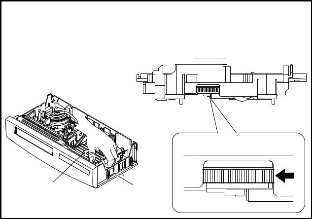
HOW TO EJECT MANUALLY
1.Remove the Top Case.
2.Rotate the roulette in the direction of the arrow as shown below.
3.Pull the tray slowly with a hand.
View for A
Rotate this roulette in the direction of the arrow
DVD Mecha |
A |
1-6-5 |
H9773DC |
Downloaded from www.Manualslib.com manuals search engine
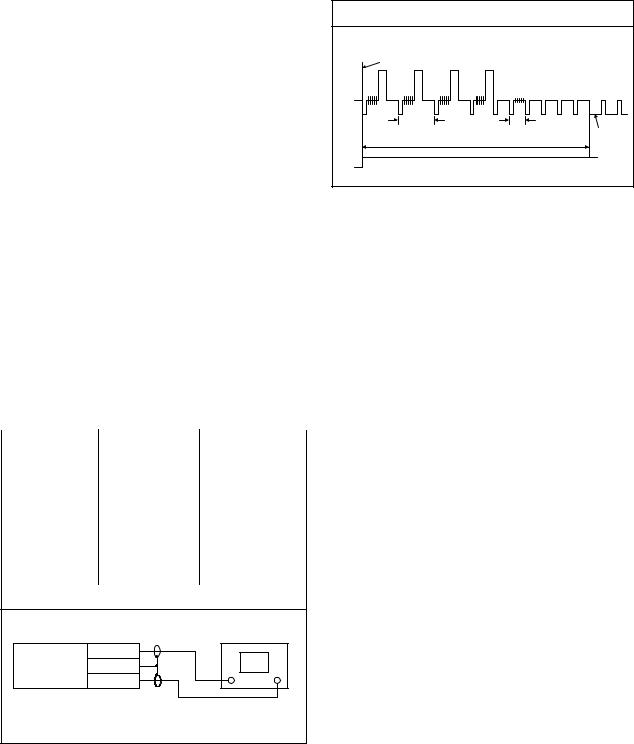
ELECTRICAL ADJUSTMENT INSTRUCTIONS
General Note: "CBA" is an abbreviation for "Circuit Board Assembly."
NOTE:
1.Electrical adjustments are required after replacing circuit components and certain mechanical parts. It is important to do these adjustments only after all repairs and replacements have been completed. Also, do not attempt these adjustments unless the proper equipment is available.
2.To perform these alignment / confirmation procedures, make sure that the tracking control is set in the center position: Press either "CHANNEL L5??" or "CHANNEL K" button on the front panel first, then the "PLAY" button on the front panel.
Test Equipment Required
1.Oscilloscope: Dual-trace with 10:1 probe, V-Range: 0.001~50V/Div.,
F-Range: DC~AC-20MHz 2.Alignment Tape (FL6A)
Head Switching Position Adjustment
Purpose:
To determine the Head Switching position during playback.
Symptom of Misadjustment:
May cause Head Switching noise or vertical jitter in the picture.
Test point |
Adj.Point |
Mode |
Input |
|
|
|
|
|
|
TP751(V-OUT) |
VR501 |
PLAY |
|
|
TP504(RF-SW) |
(Switching Point) |
----- |
||
(SP) |
||||
GND |
(MAIN CBA) |
|
||
|
|
|||
|
|
|
|
Tape |
Measurement |
Spec. |
|
Equipment |
|||
|
|
||
|
|
|
|
FL6A |
Oscilloscope |
6.5H±1H |
|
(416 s±64 s) |
|||
|
|
||
|
|||
Connections of Measurement Equipment |
|||
Oscilloscope
TP751
Main CBA GND
TP504
CH1 CH2
Trig. (+)
|
Figure 1 |
|
|
EXT. Syncronize Trigger Point |
|
CH1 |
1.0H |
0.5H |
|
||
CH2 |
6.5H±1H (416 s±64 s) |
V-Sync |
|
||
|
|
|
|
Switching Pulse |
|
Reference Notes:
Playback the Alignment tape and adjust VR501 so that the V-sync front edge of the CH1 video output waveform is at the 6.5H±1H (416 s±64 s) delayed position from the rising edge of the CH2 head switching pulse waveform.
1-7-1 |
H9700EA |
Downloaded from www.Manualslib.com manuals search engine
FIRMWARE RENEWAL MODE
1.Turn the power on and remove the disc on the tray.
2.To put the DVD player into version up mode, press [9], [8], [7], [6], and [SEARCH MODE] buttons on the remote control unit in that order. The tray will open automatically.
Fig. a appears on the screen and Fig. b appears on the VFD.
"*******" differ depending on the models.
F/W Version Up Mode |
Model No : ******* |
|
VERSION : *.** |
Please insert a DISC
for F/W Version Up.
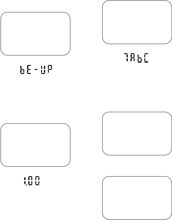
5.After programming is finished, the tray opens automatically. Fig. e appears on the screen and the checksum in (*2) of Fig. e appears on the VFD. (Fig. f)
"*******" differ depending on the models.
Model No : *******
VERSION : *.**
VERSION : D5****_****.ab5
Completed
SUM : 7ABC (*2)
EXIT: POWER
Fig. a Version Up Mode Screen
Fig. b VFD in Version Up Mode
The DVD player can also enter the version up mode with the tray open. In this case, Fig. a will be shown on the screen while the tray is open.
3.Load the disc for version up.
4.The DVD player enters the F/W version up mode automatically. Fig. c appears on the screen and Fig. d appears on the VFD. If you enter the F/W for different models, “Disc Error” will appear on the screen, then the tray will open automatically.
"*******" differ depending on the models.
F/W Version Up Mode |
Model No : ******* |
|
VERSION : *.** |
VERSION : D5****_****.ab5
Reading...(*1)
Fig. c Programming Mode Screen
Fig. d VFD in Programming Mode (Example)
The appearance shown in (*1) of Fig. c is described as follows:
No. |
Appearance |
State |
1 |
Reading... |
Sending files into the memory |
2 |
Erasing... |
Erasing previous version data |
3 |
Programming... |
Writing new version data |
Fig. e Completed Program Mode Screen
Fig. f VFD upon Finishing the Programming Mode (Example)
At this time, no buttons are available.
6.Remove the disc on the tray.
7.Unplug the AC cord from the AC outlet. Then plug it again.
8.Turn the power on by pressing the [FUNCTION] button and the tray will close.
9.Press [1], [2], [3], [4], and [DISPLAY] buttons on the remote control unit in that order.
Fig. g appears on the screen.
"*******" differ depending on the models.
MODEL : *******
Version : *.**
Region : *
EEPROM CLEAR : CLEAR EXIT: POWER
Fig. g
10.Press [CLEAR] button on the remote control unit. Fig. h appears on the screen.
"*******" differ depending on the models.
MODEL : *******
Version : *.**
Region : *
EEPROM CLEAR : OK
EEPROM CLEAR : CLEAR EXIT: POWER
Fig. h
When “OK” appears on the screen, the factory default will be set. Then the firmware renewal mode is complete.
11.To exit this mode, press [FUNCTION] button.
1-8-1 |
H9700TEST |
Downloaded from www.Manualslib.com manuals search engine
engine search manuals com.Manualslib.www from Downloaded
1-9-1
H9776BLS
|
|
|
|
|
|
|
|
|
|
|
|
|
|
|
|
|
|
|
|
|
|
Comparison Chart of |
ControlServo/System |
BLOCK |
||||
|
|
|
|
|
|
|
|
|
|
|
|
|
|
|
|
|
|
|
|
|
|
Models & Marks |
|
|
||||
|
|
|
|
|
|
|
|
|
|
|
|
|
|
|
|
|
|
|
|
|
|
|
|
Model |
Mark |
|
|
|
|
|
|
|
|
|
|
|
|
|
|
|
|
|
|
|
|
|
|
|
|
|
|
DPVR-5505 |
A |
|
|
||
|
|
|
|
|
|
|
|
|
|
|
|
|
|
|
|
|
|
|
|
|
|
|
DPVR-5505V |
B |
|
|
||
(DECK ASSEMBLY) |
|
|
|
|
|
|
|
|
|
|
|
|
|
|
|
|
|
|
|
|
|
DPVR-5805 |
C |
|
|
|||
|
|
|
|
|
SW507 |
|
|
|
|
|
|
|
IC501 |
|
|
|
|
|
TP501 |
|
|
|
|
|
|
|
|
|
|
|
|
|
|
|
|
|
|
MAIN CBA |
|
(SERVO/SYSTEM CONTROL) |
|
|
SENS-INH |
|
|
|
POWER SW CBA |
|
|
||||||||
|
|
|
|
|
LD-SW |
|
|
|
|
|
|
|
|
|
|
|
|
|
||||||||||
AC HEAD |
|
|
|
|
|
|
|
|
|
|
|
|
|
|
|
|
|
|
|
|
|
|
SW651 |
|
|
|
||
|
|
|
|
|
|
|
|
|
|
|
|
|
|
|
|
|
|
|
|
|
|
|
|
|
|
|||
ASSEMBLY |
|
|
|
|
|
|
|
|
|
|
|
|
|
|
KEY- 2 |
8 |
KEY SWITCH |
CN509 |
|
CN508 |
POWER |
|
|
|
||||
|
|
|
CN504 |
|
|
AL+5V |
|
|
|
|
|
|
9 |
LD-SW |
|
|
|
|
|
|
||||||||
|
|
|
|
|
|
|
|
|
|
|
|
KEY- 1 |
7 |
|
|
KEY SWITCH |
1 |
KEY-1 |
1 |
|
|
|
|
|
||||
CONTROL |
5 |
CL504 |
|
|
|
|
|
|
|
|
|
95 |
CTL(+) |
|
|
|
|
|
|
|
|
|
|
|
|
|
|
|
CTL(+) |
|
|
|
|
|
|
|
|
|
|
A,B |
|
|
|
|
3 |
POWER-LED 3 |
|
D651 |
AL+5V |
|
|
||||||
HEAD |
|
6 |
CTL(-) |
|
|
|
|
|
|
|
|
|
94 CTL(-) |
|
|
|
|
|
|
|
|
|||||||
|
|
|
|
|
|
|
|
|
|
|
|
|
|
D501 |
TIMER |
|
|
|
|
|
|
|||||||
|
|
|
|
|
|
|
|
|
|
|
|
|
Q502 |
|
|
|
|
POWER |
|
|
||||||||
|
|
|
|
|
|
|
|
|
|
|
|
|
10 ST-S |
|
TIMER-LED 25 |
|
|
|
|
|
|
|
||||||
|
|
|
|
|
|
|
|
|
|
|
|
|
|
|
|
|
|
|
|
|
|
|
||||||
|
|
|
|
|
|
|
|
|
|
|
|
|
|
|
|
|
|
|
|
|
|
|
|
|
||||
|
|
|
|
|
|
|
|
|
|
|
|
|
4 |
END-S |
|
|
|
|
D504 |
REC |
|
|
|
|
|
|
|
|
|
|
|
TP502 |
|
AL+5V |
|
|
|
|
|
|
|
80 |
T-REEL |
|
|
26 |
Q511 |
|
|
|
|
|
|
|
|
||
|
|
|
|
|
|
|
|
|
|
|
|
REC-LED |
|
|
|
|
|
|
|
|
|
|
||||||
|
|
|
|
|
|
|
|
|
|
|
|
|
|
|
|
|
|
|
|
|
|
|
||||||
|
|
|
END-S |
|
|
|
|
|
|
|
79 S-REEL |
|
|
|
|
|
|
|
|
|
|
|
|
|||||
|
|
|
|
Q506 |
PS502 |
|
|
Q515 |
|
|
|
|
|
|
|
|
|
|
|
|
|
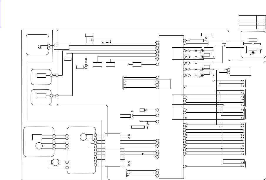
DiagramBlock |
|
|||||
|
|
|
|
|
|
|
|
|
|
|
POWER-LED 23 |
Q507 |
|
|
|
|
|
|
|
|
DIAGRAMS |
|||||||
|
|
|
|
|
|
|
|
|
|
|
|
|
|
|
|
|
|
|
|
|
|
|
||||||
|
|
|
|
D555 |
|
T-REEL |
|
S-REEL |
TIMER+5V |
RESET |
|
34 |
RESET |
|
|
|
|
|
|
|
|
|
||||||
|
|
|
|
|
|
|
|
|
|
|
|
|
|
IC502 (MEMORY) |
|
|
||||||||||||
|
|
|
|
S-LED |
|
|
|
|
|
|
|
|
|
|
|
|
Q508 |
D502 |
DVD |
|
|
|
|
|
||||
|
|
|
|
|
|
|
|
|
|
|
|
|
|
DVD-LED |
29 |
|
|
|
|
|
|
|
|
|||||
|
|
|
|
|
|
|
|
|
|
|
|
|
|
|
|
|
|
5 |
SDA |
|
|
|
|
|
|
|||
|
|
|
|
|
|
|
|
|
|
|
|
|
|
|
|
|
|
|
|
|
|
|
|
|
||||
|
Q504 |
|
|
|
|
|
|
|
|
|
|
|
|
|
|
|
|
|
|
|
|
|
|
|
|
|
||
|
|
|
|
|
|
|
|
|
|
|
|
|
|
|
|
|
Q509 |
D503 |
VCR |
6 |
SCL |
|
|
|
|
|
|
|
|
|
|
|
|
|
|
|
|
|
|
|
|
|
|
|
|
|
|
|
|
|
|
|
|||||
|
ST-S |
|
|
|
|
|
|
|
|
|
|
|
|
|
|
VCR-LED 30 |
|
|
|
|
|
|
|
|
||||
|
|
|
|
|
|
|
|
|
REMOTE-VIDEO |
|
|
|
|
|
|
|
|
|
|
|
|
|
||||||
|
|
|
|
|
|
|
|
|
|
|
|
|
|
|
|
|
|
|
|
|
|
|
||||||
|
|
|
|
|
|
|
|
|
|
14 |
REMOTE-VIDEO |
|
|
|
|
|
|
|
|
|
|
|
|
|||||
|
|
|
|
|
|
|
|
|
|
|
|
|
|
|
|
|
IIC-BUS SDA |
|
|
|
|
|
|
|||||
|
|
|
|
|
|
|
TO DVD SYSTEM |
DISPLAY-CLK |
|
|
|
C |
|
|
|
AL+5V |
|
|
|
|
|
|
||||||
SENSOR CBA |
|
|
|
|
|
|
|
|
|
|
|
IIC-BUS SCL |
|
|
|
|
|
|
||||||||||
|
|
|
|
|
CONTROL BLOCK |
|
70 |
DRV-CLK |
|
|
|
|
|
|
TO AUDIO |
|
|
|
||||||||||
|
|
|
|
|
DISPLAY-DATA |
|
|
|
|
|
|
|
|
|
|
|
||||||||||||
|
|
|
|
|
|
|
DIAGRAM |
|
|
68 |
DRV-DATA |
|
|
|
|
|
|
|
A-MUTE-H |
|
BLOCK DIAGRAM |
|
|
|||||
|
|
|
|
|
|
|
|
|
|
|
|
A-MUTE-H |
83 |
|
|
|
|
|
|
|
||||||||
|
|
|
|
|
|
|
<DVD SECTION> |
DISPLAY-STB |
|
|
|
|
|
|
|
|
|
|
|
|
||||||||
|
|
|
|
|
|
|
|
69 |
DRV-STB |
|
|
|
|
|
|
|
|
|
|
|
|
|||||||
|
|
|
|
|
|
|
|
|
|
|
|
|
|
|
|
|
|
|
IIC-BUS SDA |
|
|
|
|
|
|
|||
|
|
|
|
|
|
|
|
|
|
|
|
|
|
|
|
|
|
|
|
|
|
|
|
|
|
|
||
|
Q503 |
|
|
|
|
|
|
|
|
|
|
|
|
|
|
|
|
|
|
|
IIC-BUS SCL |
|
|
|
|
|
|
|
|
|
|
|
|
|
|
|
|
|
|
|
|
|
|
|
|
|
|
|
|
|
|
|
|
|
|
|
|
|
END-S |
|
|
|
|
|
|
|
|
|
|
|
|
|
C |
Hi-Fi-H-SW |
19 |
|
|
|
|
Hi-Fi-H-SW |
|
TO Hi-Fi AUDIO |
|
|
||
|
|
|
|
|
|
|
|
|
|
|
|
|
|
|
|
|
|
|
|
|
|
|||||||
|
|
|
|
|
|
|
|
|
|
|
|
|
|
|
|
|
|
|
|
|
|
|
|
|||||
|
|
|
|
|
|
|
|
|
|
|
|
|
|
|
|
|
|
|
|
A-MODE |
|
BLOCK DIAGRAM |
|
|
||||
|
|
|
|
|
|
|
|
|
|
|
|
|
|
|
|
A-MODE |
32 |
|
|
|
|
|
|
<VCR |
||||
|
|
|
|
|
|
|
|
|
|
|
|
|
|
|
|
|
|
|
|
LINE-MUTE |
|
|
|
|
|
|||
SENSOR CBA |
|
|
|
|
|
|
|
|
|
|
|
|
|
|
LINE-MUTE |
28 |
|
|
|
|
|
|
|
|
|
|||
|
|
|
|
|
|
|
|
|
|
|
|
|
|
|
|
|
OUTPUT SELECT |
|
|
|
|
|
||||||
|
|
|
|
|
|
|
|
|
|
|
|
|
|
|
|
|
|
|
|
|
|
|
||||||
|
|
|
|
|
|
|
|
|
|
|
|
|
|
|
|
|
|
|
|
|
|
|
|
|
|
|
||
|
|
|
|
|
|
|
|
|
|
|
TP503 |
|
A,B |
|
|
|
|
|
|
AUDIO-SW1 |
|
|
|
|
|
|
||
|
|
|
|
|
|
|
|
|
|
|
AL+5V |
CTL |
97 |
CTL |
|
AUDIO-SW1 |
62 |
|
|
|
|
|
|
|
|
|
|
|
|
|
|
|
|
|
|
|
|
|
|
|
|
|
|
|
AUDIO-SW2 |
|
|
|
|
|
|
||||||
|
|
|
|
|
|
|
|
|
|
|
|
|
|
|
|
AUDIO-SW2 |
63 |
|
|
|
|
|
TO AUDIO |
|
|
|
||
|
|
|
|
|
|
|
|
|
VR501 |
|
|
|
|
|
|
|
|
OUTPUT SELECT |
|
|
|
|
||||||
|
|
|
|
|
|
|
|
|
|
|
2 |
PG-DELAY |
|
|
|
|
|
|
|
BLOCK DIAGRAM |
|
|
||||||
|
|
|
|
|
|
|
|
|
SW-POINT |
|
|
|
|
|
|
|
|
|
|
|
|
|||||||
|
|
|
|
|
|
|
|
|
|
|
|
|
|
|
|
|
FRONT-AV |
|
|
|
|
|
|
|||||
|
|
|
|
|
|
|
|
|
|
|
|
|
FRONT-AV 20 |
|
|
|
|
|
|
|
|
|
|
|||||
|
|
|
|
|
|
|
|
|
|
|
|
|
|
|
|
|
|
|
|
|
|
|
|
|
|
|||
|
|
|
|
|
|
|
|
|
|
|
|
|
|
|
|
|
|
|
|
|
|
|
|
|
|
SECTION> |
||
|
|
|
|
|
|
|
|
|
|
|
AL+5V |
|
31 |
REC-SAF-SW |
|
|
|
|
INPUT-SELECT |
|
|
|
|
|
||||
|
|
|
|
|
|
|
|
|
|
|
SW506 |
|
|
IIC-BUS SDA |
72 |
|
|
|
IIC-BUS SDA |
|
|
|
|
|
|
|||
|
|
|
|
|
|
|
|
|
|
|
REC-SAFETY |
|
|
|
IIC-BUS SCL |
71 |
|
|
|
IIC-BUS SCL |
|
|
|
|
|
|
||
CYLINDER ASSEMBLY |
|
|
CAPSTAN MOTOR |
|
|
|
|
|
|
|
|
|
|
D-REC-H |
33 |
|
|
|
|
D-REC-H |
|
|
|
|
|
|
||
|
|
|
|
|
|
|
|
CN502 |
|
|
|
|
|
|
|
RF-SW |
18 |
|
|
|
|
RF-SW |
|
|
|
|
|
|
PG |
|
|
|
|
|
|
1 |
AL+20.5V/+12V |
|
AL+20.5V/+12V |
|
|
|
C-ROTA |
15 |
|
|
|
|
C-ROTA |
|
|
|
|
|
|
||
SENSOR |
|
|
CAPSTAN |
M |
|
2 |
P-ON+5V |
|
|
P-ON+5V |
|
|
|
|
D-V-SYNC |
13 |
|
|
|
|
D-V-SYNC |
|
TO VIDEO |
|
|
|
||
|
|
MOTOR |
|
|
|
|
|
|
|
|
|
|
|
H-A-SW |
|
BLOCK DIAGRAM |
|
|
||||||||||
|
|
|
|
|
|
3 |
C-FG |
|
|
|
|
87 |
C-FG |
|
H-A-SW |
16 |
|
|
|
|
|
|
|
|||||
|
|
|
|
|
|
|
|
|
|
|
|
|
|
|
|
H-A-COMP |
|
|
|
|
|
|
||||||
|
|
|
|
|
|
|
4 |
C-F/R |
|
|
|
|
78 C-F/R |
|
H-A-COMP |
17 |
|
|
|
|
|
|
|
|
|
|
||
DRUM |
M |
|
|
|
|
|
|
|
|
|
|
|
|
|
|
V-ENV |
|
|
|
|
|
|
||||||
|
|
|
|
|
5 |
C-CONT |
|
|
|
|
76 C-CONT |
|
V-ENV |
6 |
|
|
|
|
|
|
|
|
|
|
||||
MOTOR |
|
|
|
|
|
|
|
|
|
|
|
|
|
OUTPUT-SELECT |
|
|
|
|
|
|
||||||||
|
|
|
|
|
6 |
GND |
|
|
|
|
|
OUTPUT-SELECT |
82 |
|
|
|
|
|
|
|
|
|
||||||
|
|
|
|
|
|
|
|
|
|
|
|
|
|
|
|
C-SYNC |
|
|
|
|
|
|
||||||
|
|
|
|
|
|
|
7 |
LM-FWD/REV |
|
|
|
81 LM-FWD/REV |
C-SYNC |
58 |
|
|
|
|
|
|
|
|
|
|
||||
|
|
|
|
|
|
|
|
|
|
|
|
|
|
|
|
|
|
|
|
|
||||||||
|
|
|
|
|
|
|
8 |
D-CONT |
|
|
|
|
77 D-CONT |
INPUT-SELECT 41 |
|
|
|
|
|
|
|
|
|
|
|
|||
|
|
|
|
|
|
|
9 |
D-PFG |
|
|
|
|
90 |
D-PFG |
|
|
|
|
|
|
|
|
|
C |
|
|
|
|
|
|
|
|
|
|
|
10 GND |
|
|
|
|
|
|
|
|
|
|
|
|
|
|
|
|
|
|
|
||
|
|
M |
|
|
|
|
|
|
|
|
|
|
|
|
|
|
|
|
OUTPUT-SELECT |
|
TO DVD SYSTEM |
|
|
|||||
|
|
|
|
|
|
11 AL+12V(2) |
|
|
AL+12V(2) |
|
|
|
|
|
|
|
|
|
|
|
|
|||||||
|
LOADING |
|
|
|
|
|
|
|
|
|
|
|
|
|
|
|
|
|
|
CONTROL BLOCK |
|
|
||||||
|
MOTOR |
|
|
|
|
|
12 P-ON+15V |
|
|
P-ON+15V |
|
|
|
DVD-POWER |
21 |
|
|
|
DVD-POWER |
|
DIAGRAM |
|
|
|
||||
|
|
|
|
|
|
|
|
|
|
|
|
|
|
|
|
|
|
|
|
|
<DVD SECTION> |
|
|
|||||
|
|
|
|
|
|
|
|
TO POWER |
|
C-POW-SW |
66 |
C-POW-SW |
|
|
|
|
|
|
|
|
|
|
|
|
|
|||
|
|
|
|
|
|
|
|
|
P-ON-H |
|
|
|
|
|
|
|
|
|
|
|
|
|
|
|||||
|
|
|
|
|
|
|
|
|
|
67 |
P-ON-H |
|
|
|
|
|
|
|
|
|
|
|
|
|
|
|||
|
|
|
|
|
|
|
|
SUPPLY BLOCK |
|
|
|
|
|
|
|
|
|
|
|
|
|
|
|
|
||||
|
|
|
|
|
|
|
|
|
P-DOWN-L |
|
|
|
|
|
|
|
|
|
|
|
|
|
|
|
||||
|
|
|
|
|
|
|
|
DIAGRAM |
|
|
86 |
P-DOWN-L |
|
|
|
|
|
|
|
|
|
|
|
|
|
|
||
|
|
|
|
|
|
|
|
|
|
|
|
|
|
|
|
|
|
|
|
|
|
|
|
|
||||
|
|
|
|
|
|
|
|
|
|
|
|
|
|
|
|
|
|
|
|
|
|
|
|
|
|
|
||
engine search manuals com.Manualslib.www from Downloaded
2-9-1
H9776BLV
|
|
|
|
Comparison Chart of |
|
|
|
|
|
Models & Marks |
|
|
|
|
|
Model |
Mark |
|
|
|
|
DPVR-5505 |
A |
|
|
|
|
DPVR-5505V |
B |
|
REC-VIDEO SIGNAL |
PB-VIDEO SIGNAL |
DVD VIDEO SIGNAL MODE: SP/REC |
DPVR-5805 |
C |
IIC-BUS SDA |
TO SERVO/SYSTEM |
|
MAIN CBA |
|
|
|
|
|
|
||
IIC-BUS SCL |
CONTROL BLOCK |
|
|
|
|
|
DIAGRAM |
|
|
|
|
|
|
|
IC501 (OSD) |
|
|
|
|
|
TU701 (TUNER UNIT) |
|
|
OSD |
|
|
|
|
|
|
|
|
|
|
|
|
|
|
VIDEO |
6 |
52 |
CHARACTER |
50 |
|
|
|
|
|
MIX |
|
|
|
|
|
||
TU-VIDEO |
24 |
|
|
|
|
|
|
|
|
|
|
|
|
|
|
||
|
|
A,B |
IC301 |
|
|
|
|
|
|
|
|
|
|
|
|
78 79 |
|
|
|
J901 |
(Y/C SIGNAL PROCESS) |
65 |
68 69 |
46 |
43 |
|
IC1404 |
|
|
SERIAL |
|
|
|
|
|
|
|
|
(DECK ASSEMBLY) |
|
(INPUT SELECT) |
|
|
DECORDER |
Y. DELAY |
|
|
|
|
|
|
|
|
|
5 |
|
|
|
|
|
|
|
|
|
|
|
|
FRONT JK752 |
|
|
|
|
|
|
|
|
|
|
|
CYLINDER ASSEMBLY |
|
4 |
|
|
|
|
|
|
|
|
|
CN251 |
|
||
V-IN |
3 |
|
|
|
|
|
|
|
|
|
|
|
|
|
SW CTL |
TUNER |
|
|
|
|
|
|
|
96 |
V(R)-1 |
1 |
VIDEO (R)-1 |
|
BYPASS |
AGC |
LUMINANCE |
R |
|
P |
|
V-COM |
2 |
HEAD |
|||
C |
48 |
IN1 |
|
|
SP |
SP |
95 |
|
|
|
|||
|
|
|
SIGNAL |
|
|
V(L)-1 |
3 |
|
|||||
|
50 |
|
|
|
|
|
HEAD |
VIDEO (L)-1 |
|||||
|
IN2 |
|
|
PROCESS |
|
|
|
94 |
|
|
|||
|
9 |
|
|
|
|
EP |
AMP |
V(L)-2 |
4 |
HEAD |
|||
|
52 |
FRT |
|
|
|
|
|
93 |
|||||
|
|
|
|
|
|
|
|
V-COM |
5 |
|
|||
|
54 |
|
|
|
|
|
|
|
VIDEO (L)-2 |
||||
|
|
|
|
|
|
|
|
|
|
||||
TO |
56 |
IN2 |
|
|
|
|
|
|
|
|
V(R)-2 |
6 |
HEAD |
|
|
|
|
|
|
|
|
|
|
|
|||
SERVO/SYSTEM |
INPUT-SELECT |
FRT |
|
|
|
|
|
|
|
|
|
|
VIDEO (R)-2 |
CONTROL BLOCK |
|
PB/EE |
|
|
|
|
|
|
|
90 |
|
|
HEAD |
DIAGRAM |
|
|
|
|
|
|
|
EP |
WF1 |
|
|
||
|
|
|
CHARA. |
|
|
|
|
89 |
|
|
|||
TO DVD |
|
MUTE |
|
CCD 1H DELAY |
|
|
|
HEAD |
TP504 |
|
|
||
|
|
Y |
|
|
|
|
|
||||||
|
|
|
INS. |
|
|
88 |
|
|
|||||
DVD-VIDEO |
|
|
|
|
|
AMP |
|
|
|
||||
VIDEO/AUDIO |
TUNER |
|
|
|
|
REC FM |
RF-SW |
|
|
||||
|
|
|
|
|
+ |
|
87 |
|
|
||||
BLOCK DIAGRAM |
|
|
|
|
|
|
|
|
|
|
|||
|
IN1 |
|
1/2 |
|
|
AGC |
|
|
|
|
|||
<DVD SECTION> |
|
|
|
C |
|
|
|
D-REC-H |
|
|
|||
|
PB/EE |
|
|
|
|
|
D-REC-H |
80 |
|
|
|||
|
|
|
|
|
|
|
|
|
|
|
RF-SW
|
|
|
|
JK101 |
|
MUTE |
|
CHROMINANCE |
|
|
RF-SW/C-ROTA |
70 |
C-ROTA |
|
|
|
|
|
|
|
|
|
|
|
|
|
|||||
|
|
|
V-OUT1 |
19 |
|
|
|
|
|
D-V-SYNC |
|
||||
|
|
|
|
|
FBC |
SIGNAL |
|
|
|
D-V-SYNC |
62 |
TO SERVO/SYSTEM |
|||
|
|
|
V-IN1 |
20 |
|
|
PROCESS |
|
|
H-A-SW |
CONTROL BLOCK |
||||
|
|
|
|
|
|
P R |
P |
H-A-SW |
71 |
||||||
|
|
|
|
|
|
|
|
|
R |
H-A-COMP |
DIAGRAM |
||||
|
|
|
|
|
|
|
|
|
|
|
|
H-A-COMP |
83 |
|
|
|
|
|
|
|
|
|
|
|
|
|
|
V-ENV |
|
||
|
|
|
|
|
|
|
R |
P |
|
|
|
V-ENV |
84 |
|
|
|
|
|
|
|
|
|
|
|
|
C-SYNC |
|
||||
|
|
|
|
|
|
|
|
Y/C |
|
|
|
C-SYNC |
67 |
|
|
|
JK1402 CN2018 |
CN2017 |
|
61 |
|
MIX |
|
|
|
|
|
||||
|
|
|
|
|
|
|
|
|
|
||||||
|
|
|
|
|
AGC |
VXO |
|
|
|
|
|
|
|||
V-OUT2 |
19 |
BUFFER |
8 V-OUT2 |
8 |
|
63 |
|
|
|
|
|
|
|||
|
|
|
|
|
|
|
|
|
|
||||||
V-IN2 |
20 |
Q103 |
10 V-IN2 |
10 |
|
|
|
|
|
|
|
|
|
|
|
|
|
|
|
Q104 |
|
58 |
59 |
28 |
29 |
|
21 |
|
|
|
|
|
|
JACK-A CBA |
|
|
|
|
|
|
|
|
|
|
|
|
|
|
|
|
BUFFER |
|
|
|
|
|
|
|
|
|
|
|
|
|
|
|
|
|
|
|
|
|
|
|
|
|
|
|
|
|
|
|
|
|
IC751 |
|
|
X301 |
|
TP301 |
|
|
|
|
|
|
|
|
|
|
(OUTPUT SELECT) |
|
|
C-PB |
|
|
|
|
|||
|
|
|
|
|
|
4.43MHz |
|
|
|
|
|||||
|
|
|
|
|
|
DVD |
|
|
|
|
|
||||
|
|
|
|
|
|
|
|
|
|
|
|
|
|||
|
|
|
|
|
|
|
|
|
|
WF2 |
|
|
|
|
|
|
|
|
|
4 |
|
3 |
|
|
|
|
|
|
|
|
|
|
|
|
|
|
VCR |
|
|
|
|
|
|
|
|
|
|
|
|
|
|
|
|
5 |
|
|
|
|
|
|
|
|
|
|
|
|
|
TP751 |
SW CTL |
|
|
|
|
|
|
|
|
|
|
|
|
|
|
V-OUT |
9 |
10 11 |
|
|
|
|
|
|
|
|
|
|
|
|
|
WF3 |
|
|
|
|
|
|
|
|
|
||
|
|
|
|
|
OUTPUT-SELECT |
|
|
|
|
|
|
|
|
||
|
|
|
|
|
|
TO SERVO/SYSTEM |
|
|
|
|
|
|
|
||
|
|
|
|
|
|
|
|
|
|
|
|
|
|
|
|
|
|
|
|
|
|
|
|
CONTROL BLOCK DIAGRAM |
|
|
|
|
|
|
|
Diagram Block Video
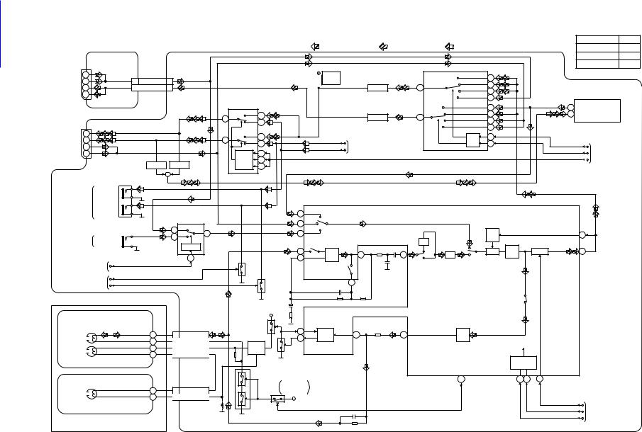
engine search manuals com.Manualslib.www from Downloaded
3-9-1
H9776BLA
Comparison Chart of
Models & Marks
|
|
|
|
|
|
|
|
|
|
|
|
|
|
|
|
|
|
Model |
Mark |
|
|
|
|
|
|
|
|
|
|
REC-AUDIO SIGNAL |
PB-AUDIO SIGNAL |
DVD AUDIO SIGNAL |
Mode : SP/REC |
DPVR-5505 |
A |
||||
|
|
JACK-A CBA |
|
|
MAIN CBA |
|
|
|
|
|
|
|
|
|
|
DPVR-5505V |
B |
||
|
|
|
|
|
|
|
|
|
|
|
|
|
|
DPVR-5805 |
C |
||||
|
JK1402 |
|
|
|
|
|
|
|
TP401 |
|
IC151 (SWITCHING) |
|
|
|
|||||
|
|
|
|
|
|
|
|
|
|
|
|
|
|
|
|||||
|
|
|
|
|
|
|
|
|
|
|
|
|
|
|
|
|
|||
A-IN2(R) |
2 |
|
CN2018 |
|
CN2017 |
|
|
|
JK1-A- |
|
|
PB/EE |
1 |
|
|
|
|
|
|
A-IN2(L) |
6 |
|
5 |
A-IN2 |
5 |
|
|
|
|
OUT(L) |
Q156 |
|
PB/EE |
|
|
|
|
|
|
|
|
|
|
|
|
5 |
|
|
|
|
|
||||||||
A-OUT2(R) |
1 |
|
1 |
A-OUT2 |
1 |
|
|
|
|
|
BUFFER |
3 |
PB/EE |
|
|
|
|
|
|
|
|
|
|
|
|
2 |
|
|
|
|
|
||||||||
A-OUT2(L) |
3 |
|
|
|
|
|
|
|
|
|
|
|
IN2 |
|
TU701(TUNER UNIT) |
|
|||
|
|
|
|
|
|
|
|
|
|
|
4 |
|
|
||||||
|
|
|
|
|
|
|
IC751 |
|
|
|
|
|
|
|
|
||||
|
|
|
|
|
|
|
|
|
|
|
|
|
|
|
|
|
|
||
|
|
|
|
|
|
|
|
|
|
|
|
TUNER |
|
|
|
|
|
|
|
|
|
|
|
|
|
|
(OUTPUT SELECT) |
|
|
|
|
12 |
|
21 AUDIO OUT |
|
||||
|
|
|
|
|
|
|
|
|
Q157 |
|
PB |
|
|
||||||
|
|
|
|
|
|
|
VCR |
|
|
|
|
|
|
||||||
|
|
|
|
|
|
|
12 |
|
|
|
14 |
|
2 |
AUDIO IN |
|
||||
|
|
|
|
|
|
|
|
|
|
13 |
IN1 |
|
|
||||||
|
|
|
|
|
|
14 |
DVD |
|
|
BUFFER |
|
|
|||||||
|
|
|
|
|
|
|
|
15 |
|
|
|
|
|
||||||
|
|
|
|
|
|
13 |
|
|
|
|
|
|
|
||||||
|
|
|
|
|
|
|
|
|
|
IN1 |
|
|
|
|
|
||||
|
JK101 |
|
|
|
|
|
|
|
|
|
|
|
|
|
|
||||
|
|
|
|
|
|
|
|
|
|
11 |
|
|
|
|
|
||||
|
|
|
|
|
|
|
|
|
|
|
|
|
|
|
|
||||
|
|
|
|
|
|
|
|
|
|
|
|
|
|
|
|
|
|||
|
|
|
|
|
|
|
|
|
|
|
|
|
|
|
|
|
|
|
|
A-OUT1(R) |
1 |
|
|
|
|
|
VCR |
2 |
|
|
|
|
SW |
10 |
|
|
|
|
|
A-OUT1(L) |
3 |
|
|
|
|
15 |
DVD |
1 |
|
DVD-A-OUT(L) |
TO DVD VIDEO/AUDIO |
CTL |
9 |
|
AUDIO-SW-1 |
|
|
||
A-IN1(R) |
2 |
|
|
|
|
|
|
|
|
DVD-A-OUT(R) |
BLOCK DIAGRAM |
|
|
|
|
AUDIO-SW-2 |
TO SERVO/ SYSTEM |
||
|
|
|
|
|
|
|
|
|
|
|
<DVD SECTION> |
|
|
|
|
||||
A-IN1(L) |
6 |
|
|
|
|
|
|
9 |
|
|
|
|
|
|
CONTROL BLOCK |
||||
|
|
|
|
Q108 |
|
Q107 |
SW |
10 |
|
|
|
|
|
|
|
OUTPUT-SELECT |
DIAGRAM |
|
|
|
|
|
|
|
BUFFER |
CTL |
|
|
|
|
|
|
|
|
|
|
|
||
|
|
|
|
BUFFER |
11 |
|
|
|
|
|
|
|
|
|
|
|
|||
|
|
|
|
|
|
|
|
|
|
|
|
|
|
|
|
||||
|
|
|
JK751 |
|
|
|
|
|
|
|
|
|
|
|
|
|
|
|
|
|
|
A-OUT(R) |
|
|
|
|
|
IC301 |
|
|
|
|
|
|
|
|
|
||
REAR |
|
|
|
|
|
|
|
|
|
|
|
|
|
|
|
|
|||
|
|
|
|
|
|
|
(AUDIO SIGNAL PROCESS) |
|
|
|
|
|
|
|
|
||||
|
|
|
|
|
|
|
|
|
|
|
|
|
|
|
|
|
|||
|
|
A-OUT(L) |
|
|
|
|
|
13 |
TUNER |
|
|
|
|
|
|
|
|
|
|
|
|
|
|
|
|
IC1404 |
|
|
|
|
|
|
|
|
|
|
|
||
|
|
|
|
|
|
|
|
|
|
|
|
|
|
|
|
|
|
||
|
|
|
|
|
|
|
|
|
IN1 |
|
|
|
|
|
|
|
|
|
|
|
|
|
|
|
|
(INPUT SELECT) |
|
|
15 |
|
|
|
|
|
|
|
|
|
|
|
|
|
|
|
12 |
14 |
|
|
17 |
IN2 |
|
|
|
ALC |
|
|
12 |
|
|
|
|
|
|
|
13 |
|
|
|
|
|
|
|
|
|
|
||||
|
|
JK754 |
|
|
|
|
|
|
|
|
DET |
|
|
|
|
||||
FRONT |
|
|
|
|
|
|
|
|
|
|
|
|
|
|
|||||
|
|
|
|
|
|
|
|
INV |
|
|
|
|
|
|
|||||
A-IN |
|
|
|
|
|
|
|
PB-ON |
|
|
|
|
|
|
|
|
|||
|
|
|
|
|
SW CTL |
|
|
|
|
|
|
|
|
|
|
|
|||
|
|
|
|
|
|
|
|
|
|
|
|
|
|
|
|
|
|||
|
|
|
|
|
|
|
|
|
|
|
R |
|
LINE |
|
|
|
|
||
|
|
|
|
|
|
|
|
5 |
EQ |
|
|
ALC |
MUTE |
11 |
|
|
|||
|
|
|
|
|
|
|
|
|
|
|
|
|
|||||||
|
|
|
|
|
|
|
|
|
8 |
9 |
ATT |
AMP |
|
|
|||||
|
|
|
|
|
|
11 |
|
|
6 |
AMP |
|
|
|
|
|
||||
TO SERVO/SYSTEM |
FRONT-AV |
|
|
|
|
|
|
P |
|
|
|
|
|
|
|||||
|
|
|
|
|
|
|
|
|
|
|
|
|
|
|
|||||
CONTROL BLOCK |
|
|
|
Q753 |
|
|
|
|
|
|
|
|
|
|
|
|
|||
|
|
|
|
|
|
SP/LP-ON |
|
|
|
|
|
|
|
|
|
||||
DIAGRAM |
|
|
|
|
|
|
|
|
|
|
|
|
|
|
|
|
|
||
|
|
|
|
|
|
|
|
|
|
|
|
|
|
|
|
|
|
||
TO DVD VIDEO/AUDIO |
A-MUTE(L) |
|
|
|
|
|
|
|
|
|
|
|
|
|
|
|
|
||
BLOCK DIAGRAM |
|
A-MUTE(R) |
|
|
|
|
Q754 |
|
|
7 |
|
|
|
|
|
|
|
|
|
<DVD SECTION> |
|
|
|
|
|
|
|
|
|
|
|
|
|
|
|
|
|
||
|
|
|
|
|
|
|
|
|
|
|
|
|
|
|
|
|
|
||
(DECK ASSEMBLY) |
|
|
|
|
|
|
|
|
|
|
|
|
REC-ON |
|
|
|
|
||
|
|
|
|
|
|
|
|
+5V |
|
|
|
|
|
|
|
|
|
|
|
AC HEAD ASSEMBLY |
|
|
|
|
|
|
|
|
|
|
|
|
|
|
|
|
|||
|
|
|
|
|
|
CN504 |
Q404 |
1 |
AUTO |
|
|
REC |
|
|
|
|
|
|
|
|
|
|
|
|
|
|
|
|
|
|
|
|
|
|
|
||||
AUDIO |
|
|
|
|
4 |
A-PB/REC |
|
|
3 |
100 |
|
|
|
|
|
|
|||
|
|
|
|
Q403 |
2 |
BIAS |
AMP |
|
|
|
|
|
|
||||||
HEAD |
|
|
|
|
3 |
A-COM |
|
|
|
|
|
|
|
|
|||||
|
|
|
|
BIAS |
|
|
|
|
|
|
|
|
|
|
|
||||
AUDIO |
|
|
|
|
1 |
AE-H |
Q406 |
|
|
|
|
|
|
|
|
|
|
||
|
|
|
|
OSC |
|
|
|
|
|
|
|
|
|
|
|||||
ERASE |
|
|
|
|
|
|
|
|
|
|
|
|
|
|
|||||
|
|
|
|
2 |
AE-H/FE-H |
|
|
|
|
|
|
|
|
|
|
||||
|
|
|
|
|
|
|
|
|
|
|
|
|
|
|
|
|
|||
HEAD |
|
|
|
|
|
|
|
|
|
|
|
|
|
|
|
|
|
||
|
|
|
|
|
|
|
|
|
|
|
|
|
|
SERIAL |
|
|
|
|
|
|
|
|
|
|
|
|
|
|
|
|
|
|
|
|
|
|
|
|
|
|
|
|
|
|
|
|
|
|
|
|
|
|
AUDIO HD-SW |
|
DECODER |
|
|
|
|
|
|
|
|
|
|
|
|
|
|
|
|
|
|
|
|
|
|
|
|
|
|
|
|
|
|
|
|
|
|
|
|
|
CONTROL |
|
|
|
|
|
|
|
FE HEAD |
|
|
CN501 |
|
|
SWITCHING |
|
|
|
16 |
|
68 69 |
71 |
|
|
|
||
FULL |
|
|
|
|
|
|
|
|
|
|
|
|
|
|
|
|
|
||
|
|
|
|
2 |
FE-H |
|
Q405 |
D-REC-OFF |
|
|
|
|
|
|
|
|
|
|
|
ERASE |
|
|
|
|
1 |
FE-H-GND |
|
|
+5V |
|
|
|
|
|
|
|
|
|
|
HEAD |
|
|
|
|
|
|
|
|
|
|
|
|
A-MUTE-H |
|
|
|
|||
|
|
|
|
|
|
|
|
|
|
|
|
|
|
|
|
|
|||
|
|
|
|
|
|
|
Q401 |
|
|
|
|
|
|
|
|
TO SERVO/SYSTEM |
|||
|
|
|
|
|
|
|
|
|
|
|
|
|
|
IIC-BUS SDA |
|
||||
|
|
|
|
|
|
|
(PB=ON) |
|
|
|
|
|
|
|
|
CONTROL BLOCK |
|||
|
|
|
|
|
|
|
|
|
|
|
|
|
|
IIC-BUS SCL |
|
||||
|
|
|
|
|
|
|
|
|
|
|
|
|
|
|
|
|
DIAGRAM |
|
|
) B A, ( Diagram Block Audio

engine search manuals com.Manualslib.www from Downloaded
4-9-1
H9778BLA
|
|
Comparison Chart of |
|
|
|
Models & Marks |
|
|
|
Model |
Mark |
|
|
DPVR-5505 |
A |
|
|
DPVR-5505V |
B |
|
|
DPVR-5805 |
C |
PB-AUDIO SIGNAL |
REC-AUDIO SIGNAL Mode : SP/REC |
||
MAIN CBA
TO Hi-Fi AUDIO |
N-A-PB |
|
|
|
|
|
|
|
|
|
|
|
|
|
N-A-REC |
|
|
|
|
|
|
|
|
|
|
|
|
|
|
BLOCK DIGRAM |
|
|
|
|
|
|
|
|
|
|
|
|
|
|
|
|
|
|
|
|
|
|
|
|
|
|
|
|
|
|
|
|
|
|
IC301 |
|
|
13 |
15 |
17 |
|
|
|
|
|
|
|
|
|
(AUDIO SIGNAL PROCESS) |
|
|
|
|
|||||
|
|
|
|
|
|
|
|
|
TUNER |
IN1 |
IN2 |
|
|
|
|
|
|
|
|
|
|
|
|
|
|
|
|
||
|
|
|
|
|
|
|
|
|
|
|
ALC |
|
|
12 |
|
|
|
|
|
|
|
|
|
|
|
DET |
|
|
|
|
|
|
|
|
|
|
|
|
INV |
|
|
|
|
|
|
|
|
|
|
|
PB-ON |
|
|
|
|
|
|
|
|
|
|
|
|
|
|
|
|
R |
|
|
LINE |
|
|
|
|
|
|
|
|
5 |
EQ |
|
|
|
ALC |
MUTE |
11 |
||
|
|
|
|
|
8 |
9 |
ATT |
|
AMP |
|||||
|
|
|
|
|
6 |
AMP |
P |
|
|
|
||||
|
|
|
|
|
|
|
|
|
|
|
|
|||
|
|
|
|
|
|
|
|
|
|
|
|
|
|
|
(DECK ASSEMBLY) |
|
|
|
|
|
SP/LP-ON |
|
|
|
|
|
|
|
|
|
|
|
|
+5V |
|
|
7 |
|
|
|
|
|
|
|
|
|
|
|
|
|
|
|
|
|
|
|
|
|
|
AC HEAD ASSEMBLY |
|
|
|
|
|
|
|
|
|
|
|
|
|
|
|
|
|
CN504 |
Q404 |
|
|
|
|
|
|
|
REC-ON |
|
|
|
|
|
|
|
|
|
|
|
|
|
|
|
||
|
|
|
|
|
|
|
|
|
|
|
|
|
|
|
AUDIO |
|
4 |
A-PB/REC |
Q403 |
|
|
|
|
|
|
|
|
|
|
HEAD |
|
3 |
A-COM |
|
|
|
|
|
|
|
|
|
|
|
|
BIAS |
|
|
|
|
|
|
|
|
|
|
|||
AUDIO |
|
1 |
AE-H |
|
|
|
|
|
|
|
|
|
|
|
|
OSC |
|
|
|
|
|
|
|
|
|
|
|||
ERASE |
|
2 |
AE-H/FE-H |
|
|
|
|
|
|
|
|
|
|
|
|
|
1 |
AUTO |
|
|
REC |
|
|
|
|
||||
HEAD |
|
|
|
|
3 |
100 |
|
|
|
|
||||
|
|
|
|
2 |
BIAS |
AMP |
|
|
|
|
||||
|
|
|
|
|
|
|
|
|
|
|
||||
|
|
|
|
Q406 |
|
|
|
|
|
|
|
|
|
|
|
|
|
|
|
|
|
|
|
|
|
|
SERIAL |
|
|
|
|
|
|
|
|
|
|
|
AUDIO HD-SW |
DECODER |
|
|||
|
|
|
|
|
|
|
|
|
|
|
|
|||
FE HEAD |
|
|
|
|
SWITCHING |
|
|
|
CONTROL |
|
|
|
|
|
|
|
|
|
|
|
|
16 |
|
|
68 69 |
71 |
|
||
|
|
|
Q405 |
D-REC-OFF |
|
|
|
|
|
|
||||
|
|
|
CN501 |
|
|
|
|
|
|
|||||
FULL |
|
|
|
+5V |
|
|
|
|
|
|
|
|
|
|
|
2 |
FE-H |
|
|
|
|
|
|
|
|
|
|
||
ERASE |
|
|
|
|
|
|
|
|
|
|
|
|
||
|
1 |
FE-H-GND |
Q401 |
|
|
|
|
|
|
|
|
|
|
|
HEAD |
|
|
|
|
|
|
|
|
|
A-MUTE-H |
|
|||
|
|
|
(PB=ON) |
|
|
|
|
|
|
|
|
|
||
|
|
|
|
|
|
|
|
|
|
|
|
TO SERVO/SYSTEM |
||
|
|
|
|
|
|
|
|
|
|
|
|
|
IIC-BUS SDA |
|
|
|
|
|
|
|
|
|
|
|
|
|
|
CONTROL BLOCK |
|
|
|
|
|
|
|
|
|
|
|
|
|
|
IIC-BUS SCL |
|
|
|
|
|
|
|
|
|
|
|
|
|
|
DIAGRAM |
|
) C ( Diagram Block Audio

from Downloaded |
|
|
|
|
|
|
|
|
|
|
|
|
|
|
|
|
|
|
|
|
|
|
|
|
|
|
|
|
|
BlockAudioFi-Hi |
searchmanualscom.Manualslib.www |
|
|
|
|
|
|
|
|
|
|
|
|
|
|
|
|
|
|
|
|
|
|
|
|
|
|
Comparison Chart of |
|||
|
|
|
|
|
|
|
|
|
|
|
|
|
|
|
|
|
|
|
|
|
|
|
|
|
|
|
Models & Marks |
|
||
|
|
|
|
|
|
|
|
|
|
|
|
|
|
|
|
|
|
|
|
|
|
|
|
|
|
|
Model |
Mark |
|
|
|
|
|
|
|
|
|
|
|
|
|
|
|
|
|
|
PB-AUDIO SIGNAL |
REC-AUDIO SIGNAL |
|
DVD AUDIO SIGNAL |
Mode : SP/REC |
DPVR-5505 |
A |
|
|||||||
|
|
|
|
|
|
|
|
|
|
|
|
|
|
|
|
|
DPVR-5505V |
B |
|
|||||||||||
|
|
|
|
|
|
|
|
|
|
|
|
|
|
|
|
|
|
|
|
|
|
|
|
|
|
|
|
|||
|
|
|
JACK-A CBA |
|
|
|
|
|
|
|
|
|
MAIN CBA |
|
|
|
|
|
IC751 |
|
|
|
TP401 |
|
DPVR-5805 |
C |
|
|||
|
|
|
|
|
|
|
|
|
|
|
|
|
|
|
|
|
|
|
|
|
|
JK1-A-OUT(L) |
|
|
|
|
|
|||
|
|
JK1402 |
|
CN2018 |
|
|
|
CN2017 |
|
|
|
|
|
|
|
|
|
(OUTPUT SELECT) |
|
|
|
|
|
|||||||
|
|
|
|
|
|
|
|
|
|
|
|
|
|
|
|
|
|
|
|
|
|
|
||||||||
|
|
|
|
|
|
|
|
|
|
|
|
|
|
|
|
|
VCR |
|
|
|
|
|
|
|
|
|||||
|
|
|
|
|
|
|
|
|
|
|
|
|
|
|
|
|
|
|
|
|
|
|
|
|
|
|
||||
|
A-IN2(R) |
2 |
|
|
4 |
A-IN2(R) |
|
4 |
|
|
|
|
|
|
|
|
|
|
|
|
12 |
|
|
|
|
|
|
|
||
|
A-IN2(L) |
6 |
|
|
5 |
A-IN2(L) |
|
5 |
|
|
|
|
|
|
|
|
|
|
14 |
|
DVD |
13 |
|
|
|
|
|
|
|
|
|
A-OUT2(R) |
1 |
|
|
1 |
A-OUT2(R) |
|
1 |
|
|
|
|
|
|
|
|
|
|
|
|
VCR |
|
|
|
|
|
|
|
|
|
|
A-OUT2(L) |
3 |
|
|
2 |
A-OUT2(L) |
|
2 |
|
|
|
|
|
|
|
|
|
|
|
|
2 |
|
|
|
|
|
|
|
||
|
|
|
|
|
|
|
|
|
|
|
|
|
|
15 |
|
DVD |
|
|
|
|
|
|
|
|||||||
|
|
|
|
|
|
|
|
|
|
|
|
|
|
|
|
|
|
|
|
|
|
|
|
|
|
|
|
|||
|
|
|
|
|
|
|
|
|
|
|
|
|
|
|
|
|
|
Q107 |
|
|
|
1 |
|
|
|
|
|
|
|
|
|
|
|
|
|
|
|
|
|
|
|
|
|
|
|
|
|
|
|
|
|
|
|
|
|
|
|
|
|
||
engine |
|
|
|
|
|
|
|
|
|
|
|
A-MUTE(L) |
|
|
|
|
|
BUFFER |
|
|
SW CTL |
|
|
|
DVD-A-OUT(L) |
BLOCK DIAGRAM |
Diagram |
|||
|
|
|
|
|
|
|
|
|
|
|
|
TO DVD VIDEO/AUDIO |
|
|
|
Q108 |
|
|
|
|
|
|
||||||||
|
|
|
|
|
|
|
|
|
|
|
|
|
|
|
|
|
|
|
|
|
|
|
|
|
|
|
||||
|
|
JK101 |
|
|
|
|
|
|
|
|
A-MUTE(R) |
BLOCK DIAGRAM |
|
|
|
BUFFER |
|
9 10 11 |
|
|
|
|
|
|
|
|
||||
|
|
|
|
|
|
|
|
|
|
|
|
<DVD SECTION> |
|
|
|
|
|
|
|
|
|
|
|
|
|
|
||||
|
|
|
|
|
|
|
|
|
|
|
|
|
|
|
|
|
|
|
|
|
|
|
|
|
|
|
|
|
||
|
A-OUT1(R) |
1 |
|
|
|
|
|
|
|
|
|
|
|
|
|
|
|
|
|
|
|
|
|
|
|
|
|
TO |
|
|
|
A-OUT1(L) |
3 |
|
|
|
|
|
|
|
|
|
|
|
|
|
|
|
|
|
|
|
|
|
|
|
OUTPUT-SELECT |
SERVO/ SYSTEM |
|
||
|
A-IN1(R) |
2 |
|
|
|
|
|
|
|
|
|
|
|
|
|
|
|
|
|
|
|
|
|
|
|
|
|
CONTROL BLOCK |
|
|
|
|
|
|
|
|
|
|
|
|
|
|
|
|
|
|
|
|
|
|
|
|
|
|
|
|
DIAGRAM |
|
|||
|
A-IN1(L) |
6 |
|
|
|
|
|
|
|
|
|
|
|
|
|
|
|
|
|
|
|
|
|
|
|
|
|
|
||
|
|
|
|
|
|
|
|
|
|
|
|
|
|
|
|
|
|
|
|
|
|
|
|
DVD-A-OUT(R) |
TO DVD AUDIO |
|
||||
|
|
|
|
|
|
|
|
|
|
|
|
|
|
|
|
|
|
|
|
|
|
|
|
|
|
|
||||
|
|
|
|
|
|
|
|
|
|
|
|
|
|
|
|
|
|
|
|
|
|
|
|
|
|
|
|
|
||
|
|
|
|
|
|
|
|
|
|
|
|
|
|
|
|
|
|
|
|
|
|
|
|
|
|
|
|
<DVD SECTION> |
( |
|
|
|
|
|
|
|
|
|
|
|
|
|
|
|
|
|
|
|
|
|
|
|
|
|
|
|
|
|
|
|
|
|
|
|
JK751 |
|
|
|
|
|
|
|
IC451 (MTS/ SAP/ Hi-Fi AUDIO PROCESS/ Hi-Fi HEAD AMP) |
|
|
|
|
|
|
|
|
|
|
|
|
|
C |
|||||
|
|
|
|
|
|
|
|
|
|
|
|
|
|
|
|
|
|
|
|
|
|
|
|
|
|
|
|
) |
||
|
A-OUT(R) |
|
|
|
|
|
|
|
|
67 |
|
|
|
|
|
|
|
|
|
|
|
|
|
|
|
|
|
|
||
|
|
|
|
|
|
|
|
|
|
|
|
|
|
|
|
|
|
|
|
|
|
|
|
|
|
|
|
|||
|
|
|
|
|
|
|
|
|
65 |
|
|
|
|
|
|
|
|
|
|
|
|
|
|
|
|
|
|
|
||
|
REAR |
|
|
|
|
|
|
|
|
|
|
|
|
|
|
|
|
|
|
|
|
|
|
|
|
|
|
|
|
|
|
|
|
|
|
|
|
|
|
|
|
SW |
|
|
|
|
|
|
|
|
|
|
|
|
|
|
|
|
|
|
|
|
A-OUT(L) |
|
|
|
|
|
|
|
|
|
|
|
|
|
|
|
|
|
|
|
|
|
|
|
|
|
|
|
||
|
|
|
|
|
|
|
|
|
|
|
|
|
|
|
|
|
|
|
|
|
|
|
|
|
|
|
|
|
||
|
5-9-1 |
|
|
|
|
|
|
|
|
|
|
|
SW |
|
|
|
|
|
|
|
|
|
|
|
|
|
|
|
|
|
|
|
|
|
|
|
|
|
|
|
|
ALC |
ALC |
|
SW |
|
COMP |
R-CH |
|
SERIAL |
|
37 |
IIC-BUS SDA |
|
|
|
|||||
|
|
|
|
|
|
|
|
|
|
|
|
NOISE |
|
BPF |
|
|
|
|
|
|
|
|||||||||
|
|
|
|
|
|
|
|
|
|
|
|
|
|
|
|
|
|
|
DATA |
|
|
|
IIC-BUS SCL |
|
|
|
||||
|
|
|
|
|
|
|
|
|
|
|
|
|
|
|
|
P |
|
|
|
|
|
|
38 |
|
|
|
||||
|
|
|
|
|
|
|
|
|
|
|
|
62 |
70 |
|
R-CH |
|
|
|
|
DECODER |
|
|
|
|
|
|
||||
|
|
|
|
|
|
|
|
|
|
|
|
|
|
|
|
|
|
|
|
|
|
|
|
|
|
|
|
|||
|
|
|
|
|
Q753 |
Q754 |
|
|
|
|
|
|
|
PNR |
R |
|
|
|
|
|
|
|
|
Q451 |
|
|
|
|
|
|
|
|
|
|
|
|
|
|
|
|
|
|
|
|
|
|
|
|
|
|
|
|
|
|
|
|
|||||
|
|
|
|
|
|
|
|
|
|
|
|
61 |
71 |
|
|
|
|
|
|
|
|
|
|
|
|
A-MODE |
|
|
|
|
|
|
|
|
|
|
|
|
|
|
|
|
|
|
|
|
|
|
|
DO |
ENV |
|
21 |
|
|
|
|
||||
|
|
JK753 |
|
|
|
|
|
|
|
|
|
|
|
|
|
|
|
|
|
|
|
|
|
|
|
|||||
|
|
|
|
|
|
|
|
|
|
|
|
|
|
|
LIM |
DEV |
VCO |
LPF |
|
DET |
DET |
|
|
|
|
|
|
|||
|
|
|
|
|
|
|
|
|
|
|
|
|
|
|
|
|
|
|
|
|
|
|
||||||||
|
|
A-IN(L) |
|
|
|
|
|
|
|
|
|
|
|
|
|
|
|
|
|
|
|
|
|
|
|
|
|
TO |
|
|
|
|
|
|
|
|
|
|
|
|
|
52 |
|
|
|
47 |
|
|
|
|
|
|
|
|
|
|
|
|
|
|
|
|
FRONT |
|
|
|
|
|
|
|
|
|
|
|
|
|
|
|
|
|
|
|
MUTE-ON |
|
|
|
SERVO/ SYSTEM |
|
||||
|
|
|
|
|
|
|
|
|
|
56 |
R-CH |
|
|
|
|
|
|
|
|
|
|
|
|
77 |
|
|
CONTROL BLOCK |
|
||
|
|
|
|
|
|
|
|
|
|
|
|
|
48 |
|
|
|
|
|
|
|
|
|
|
|
|
|||||
|
|
|
|
|
|
|
|
|
|
|
54 |
INSEL |
|
|
|
|
|
|
|
|
|
|
|
|
|
DIAGRAM |
|
|||
|
|
JK754 |
|
|
|
|
|
|
|
|
|
|
|
|
|
|
|
|
|
|
|
76 |
|
|
|
|||||
|
|
|
|
|
|
|
|
|
|
|
|
|
|
|
OUTPUT |
|
|
|
|
|
|
|
|
|
|
|
||||
|
|
|
|
|
|
|
|
|
|
|
|
|
|
|
|
|
|
|
|
|
|
|
|
|
|
|
|
|||
|
|
A-IN(R) |
|
|
|
|
|
|
|
|
50 |
|
|
|
|
|
|
|
|
|
|
|
|
|
|
|
|
|
|
|
|
|
|
|
|
|
|
|
|
|
|
|
|
|
|
|
SELECT |
|
|
|
|
|
|
|
|
|
|
|
|
||
|
|
|
|
|
|
|
|
|
|
|
58 |
|
|
|
|
|
|
|
|
|
|
|
|
74 |
|
|
|
|
|
|
|
|
|
|
|
|
|
|
|
|
|
|
|
|
|
|
|
|
|
|
|
|
|
|
|
|
|
|
|
||
|
TU701 |
|
|
|
|
|
|
|
|
|
60 |
|
|
|
|
|
|
|
|
|
|
|
|
|
|
|
|
|
|
|
|
|
|
|
|
|
|
|
|
|
|
|
|
|
|
|
|
|
|
|
|
MUTE-ON |
|
|
|
|
|
|
|||
|
(TUNER UNIT) |
|
|
|
|
|
|
|
|
|
|
|
|
|
|
|
|
|
|
|
|
|
|
|
|
|
|
|||
|
|
|
|
|
|
|
|
|
|
|
|
|
|
|
|
|
|
|
|
|
|
|
73 |
|
|
|
|
|
||
|
AUDIO |
|
|
|
|
|
|
|
|
|
2 |
|
|
|
|
|
|
|
|
|
|
|
|
|
Hi-Fi-H-SW |
|
|
|
||
|
2 |
|
|
|
|
|
|
|
|
|
|
|
|
|
|
HOLD |
|
|
|
|
|
|
39 |
|
|
|
||||
|
|
|
|
|
|
|
|
|
|
|
|
|
|
|
|
|
|
|
|
|
|
|
|
|
|
|||||
|
|
|
|
|
|
|
|
|
|
|
6 |
|
|
|
|
|
|
PULSE |
|
|
|
|
|
|
75 |
LINE-MUTE |
|
|
|
|
|
|
|
|
|
|
|
|
|
|
|
10 |
|
L-CH |
|
|
|
|
|
|
|
|
|
|
|
|
|
|
|||
|
|
|
|
|
|
|
|
|
|
|
|
|
14 |
|
|
|
|
|
|
|
|
|
53 |
|
|
|
||||
|
|
|
|
|
|
|
|
|
|
|
|
|
|
|
|
|
|
|
|
|
|
|
|
|
|
|
||||
|
|
|
|
|
|
|
|
|
|
|
8 |
|
INSEL |
|
|
NOISE |
|
|
|
|
|
|
|
|
|
|
|
|||
|
|
|
|
|
|
|
|
|
|
|
|
|
|
MIX |
COMP |
|
|
|
26 |
|
|
|
|
|
||||||
|
|
|
|
|
|
|
|
|
|
|
|
|
|
|
|
|
|
|
|
|
|
|
||||||||
|
|
|
|
|
|
|
|
|
|
|
4 |
|
|
|
15 |
|
|
DET |
|
|
|
|
(DECK ASSEMBLY) |
|
||||||
|
|
|
|
|
|
|
|
|
|
|
|
|
|
|
|
|
|
|
|
|
|
|
|
|
||||||
|
|
|
|
|
|
|
|
|
|
|
|
|
|
|
|
|
|
|
|
|
|
|
|
|
|
|||||
|
|
|
|
|
|
|
AFV CBA |
|
|
12 |
|
|
|
|
LIM |
DEV |
VCO |
LPF |
|
|
|
|
|
|
|
|
|
|
|
|
|
|
CN701 |
|
CN1 |
CN1 |
|
CN701 |
|
|
|
|
|
|
|
|
|
|
|
|
CYLINDER |
|
|||||||||
|
|
|
|
|
|
|
|
|
|
|
|
|
|
|
|
|
|
|
|
|
|
|
||||||||
|
SIF OUT 22 |
2 |
SIF |
2 |
|
IF SINAL |
|
4 |
TU-AUDIO(R) |
4 |
|
|
|
L-CH |
R |
|
|
|
|
|
|
|
|
|
|
|
ASSEMBLY |
|
||
|
|
|
|
|
|
|
|
5 |
TU-AUDIO(L) |
5 |
|
|
|
|
|
|
|
|
|
|
|
|
|
CN251 |
|
|
|
|
||
|
|
|
|
|
|
|
PROCESS |
NOR |
|
|
PNR |
P |
|
|
|
|
|
|
R |
|
|
|
|
Hi-Fi |
|
|||||
|
|
|
|
|
|
|
|
|
|
|
|
|
|
|
|
|
|
|
|
|
24 |
Hi-Fi-A(R) |
7 |
|
|
|||||
|
|
|
|
|
|
|
|
|
|
|
|
SW |
|
|
|
SW |
|
|
L-CH |
|
|
|
|
|
|
|||||
|
|
|
|
|
|
|
|
|
|
|
|
|
|
|
|
COMP |
LIM |
34 |
33 |
|
|
Hi-Fi-COM |
8 |
|
AUDIO |
|
||||
|
|
|
|
|
|
|
|
|
|
|
|
|
|
|
|
NOISE |
|
BPF |
|
|
|
(R) |
|
|||||||
|
|
|
|
|
|
|
|
|
|
|
|
|
|
|
|
|
|
|
|
|
L |
|
27 |
Hi-Fi-A(L) |
9 |
|
HEAD |
|
||
|
|
|
|
|
|
|
|
N-A-REC |
|
|
|
|
|
|
|
|
|
|
|
|
|
|
|
|||||||
|
H9778BLH |
|
|
|
TO AUDIO |
|
|
78 |
|
|
|
|
|
|
|
|
|
|
|
|
|
|
|
|
|
Hi-Fi |
|
|||
|
|
|
|
|
|
N-A-PB |
|
|
|
|
|
|
|
|
|
|
|
|
|
|
|
|
|
|
|
|||||
|
|
|
|
|
BLOCK DIAGRAM |
|
80 |
|
|
|
|
|
|
|
|
|
|
|
|
|
|
|
|
|
AUDIO |
|
||||
|
|
|
|
|
|
|
|
|
|
|
|
|
|
|
|
|
|
|
|
|
|
|
|
|
|
|
|
(L) |
|
|
|
|
|
|
|
|
|
|
|
|
|
|
|
|
|
|
|
|
|
|
|
|
|
|
|
|
|
|
|
|
|
|
|
|
|
|
|
|
|
|
|
|
|
|
|
|
|
|
|
|
|
|
|
|
|
|
|
|
|
|
HEAD |
|
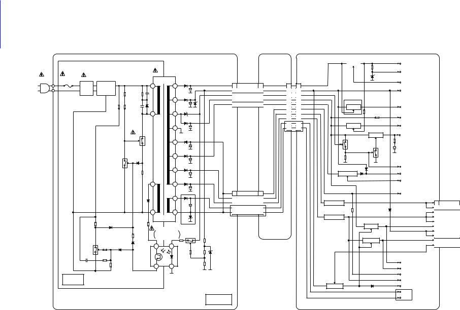
engine search manuals com.Manualslib.www from Downloaded
6-9-1
H9776BLP
|
|
|
|
|
|
|
|
Comparison Chart of |
|
|
|
|
|
|
|
|
|
Models & Marks |
|
CAUTION ! |
NOTE : |
CAUTION |
|
Model |
Mark |
||||
Fixed voltage (or Auto voltage selectable ) power supply circuit is used in this unit. |
|
||||||||
The voltage for parts in hot circuit is measured using |
FOR CONTINUED PROTECTION AGAINST FIRE HAZARD, |
|
DPVR-5505 |
A |
|||||
If Main Fuse (F1001) is blown, check to see that all components in the power supply |
|
||||||||
hot GND as a common terminal. |
|
||||||||
circuit are not defective before you connect the AC plug to the AC power supply. |
REPLACE ONLY WITH THE SAME TYPE T1.6AL/250V FUSE. |
|
|
|
|||||
|
DPVR-5505V |
B |
|||||||
|
|
|
|
|
|
|
|||
Otherwise it may cause some components in the power supply circuit to fail. |
|
|
|
|
|
|
|
||
|
|
|
|
|
|
|
DPVR-5805 |
C |
|
|
|
|
|
|
|
|
|
||
HOT CIRCUIT. BE CAREFUL. |
|
|
Q053,Q054 |
|
|
|
|||
|
|
|
SW+44V |
|
|
|
P-ON+44V |
|
|
|
|
|
|
|
|
|
|
|
|
|
|
|
|
T0011 |
|
|
|
|
|
|
|
P-ON+15V |
|
|
F1001 |
|
|
|
|
|
|
|
|
|
|
|
|
AC1001 |
L1003 |
D001 - D004 |
|
|
CL051A |
|
CL051B |
CN051A |
CN051 |
|
|
|
|
T1.6AL/250V |
|
|
|
|
P-ON-H |
|
|||||||
|
LINE |
BRIDGE |
|
|
|
|
|
||||||
|
|
2 |
20 |
1 |
AL+44V |
1 |
1 |
1 |
|
<FROM PIN 67 OF IC501> |
|
||
|
|
|
RECTIFIER |
|
|
||||||||
|
|
FILTER |
|
|
3 |
AL+12V |
3 |
3 |
3 |
|
AL+12V |
|
|
|
|
|
|
|
|
5 |
AL+5V(P-DOWN) |
5 |
5 |
5 |
C |
|
|
|
|
|
|
|
19 |
6 |
AL+5V |
6 |
6 |
6 |
|
|
|
|
|
|
|
|
Q055 |
|
|
||||||
|
|
|
|
|
|
8 |
AL+20.5V |
8 |
8 |
8 |
|
|
|
|
|
|
|
|
|
SW+9V |
AL+9V |
|
|||||
|
|
|
|
|
|
|
|
|
10 |
10 |
|
||
|
|
|
|
|
|
|
|
|
|
|
|
||
|
|
|
|
4 |
18 |
|
|
|
12 |
12 |
|
AL+5V |
|
|
|
|
|
|
|
|
|
|
14 |
14 |
Q056 |
|
|
|
|
|
|
|
|
|
|
|
|
|
|||
|
|
|
|
|
|
|
|
|
18 |
18 |
|
|
|
|
|
|
|
|
|
|
|
|
SW+5V |
P-ON+5V |
|
||
|
|
|
|
|
17 |
|
|
|
17 |
17 |
|
||
|
|
|
|
|
|
|
|
Q058 |
|
|
|||
|
|
|
|
|
|
|
|
|
|
C |
|
|
|
|
|
|
|
Q1001 |
|
|
|
|
|
SW+5V |
TIMER+5V |
|
|
|
|
|
|
|
|
|
|
|
|
|
|||
|
|
|
|
|
|
|
|
|
|
|
|
|
|
|
|
|
|
|
16 |
|
|
|
|
|
Q057 |
|
|
|
|
|
|
|
|
|
|
|
|
|
|
|
|
|
|
|
|
|
|
|
|
|
|
|
Q059 |
|
|
|
|
|
|
|
15 |
|
|
|
|
|
|
|
|
|
|
|
Q1003 |
|
|
|
|
|
|
|
|
P-DOWN-L |
|
|
|
|
|
|
|
|
|
|
|
|
|
|
|
|
|
|
|
|
14 |
|
|
|
|
|
Q051,Q052 |
<TO PIN 86 OF IC501> |
|
|
|
|
|
|
|
|
|
|
|
SW+20.5V |
AL+20.5V/+12V |
|
|
|
|
|
|
|
|
|
|
|
|
|
|
||
|
|
|
|
|
|
|
|
|
|
|
|
C-POW-SW |
|
|
|
|
|
7 |
13 |
|
|
|
|
|
|
<FROM PIN 66 OF IC501> |
|
|
|
|
|
|
|
|
|
|
|
|
|
||
|
|
|
|
|
|
CL052A |
|
CL052B |
|
|
|
|
|
|
|
|
|
|
|
1 |
AL-30V |
1 |
|
|
|
AL-30V |
|
|
|
|
|
|
12 |
3 |
AL+2.8V |
3 |
|
|
IC1002 |
CL1051 |
|
|
|
|
|
|
|
5 |
AL+4V |
5 |
|
|
+1.2V REG. |
1 |
EV+1.2V |
|
|
|
|
|
|
9 |
F1 |
9 |
|
|
|
2 |
EV+1.2V |
|
|
|
|
8 |
11 |
8 |
F2 |
8 |
|
|
IC1003 |
3 |
EV+3.3V |
|
|
|
|
|
|
C |
|
|
|
|
+3.3V REG. |
4 |
EV+3.3V |
|
|
|
|
|
|
|
|
|
|
Q1055 |
5 |
EV+3.3V |
|
|
|
|
|
|
|
|
|
|
|
|
|||
|
|
|
|
IC1001 |
|
C |
|
JUNCTION |
|
SW+5V |
7 |
P-ON+5V |
|
|
|
|
|
|
|
|
|
|
8 |
EV+11V |
|||
|
|
|
|
ERROR |
|
|
|
CBA |
|
|
|
||
|
|
|
|
|
Q1004 |
|
|
|
Q1052 |
9 |
EV+11V |
||
|
|
|
|
VOLTAGE DET |
|
|
|
|
|||||
|
|
|
|
|
|
|
|
|
|
|
SW+3.3V |
6 |
P-ON+3.3V |
|
|
|
|
4 |
1 |
|
|
|
|
|
|
17 PWRCON |
|
|
|
Q1008 |
|
|
|
|
|
|
|
|
|
||
|
|
|
|
|
|
|
|
|
|
|
|
|
|
|
|
|
|
3 |
2 |
|
|
|
|
|
|
DVD P-ON+5V |
|
|
|
|
|
|
|
|
|
|
|
DVD P-ON+3.3V |
|
||
|
|
|
|
|
|
|
|
|
|
|
|
|
|
|
HOT |
|
|
|
|
|
|
|
|
Q1053, |
-FL |
|
|
|
|
|
|
|
|
|
|
|
EV+3.3V |
|
|||
|
|
|
|
|
|
|
|
|
Q1054 |
|
|||
|
|
|
|
|
|
|
|
|
|
|
SW+12V |
DVD P-ON+12V |
|
|
|
|
|
|
|
COLD |
|
|
|
|
|
F1 |
|
|
|
|
|
|
|
|
|
|
|
|
C |
|
|
|
|
|
|
|
|
|
|
|
|
|
|
F2 |
|
|
|
|
POWER SUPPLY CBA |
|
|
|
|
|
|
MAIN CBA |
|
|
|
Diagram Block Supply Power

engine search manuals com.Manualslib.www from Downloaded
7-9-1
H9776BLSD
|
|
|
|
|
|
|
|
|
|
Comparison Chart of |
|
|
|
|
|
|
|
|
|
|
|
||
|
|
|
|
|
|
|
MODEL |
A, B |
C |
Models & Marks |
|
|
|
|
|
|
|
MARK |
|
|
Model |
Mark |
|
|
|
|
|
|
|
|
|
PLAY |
FP-CLK |
DPVR-5505 |
A |
|
|
|
|
|
|
|
|
SKIP-DOWN FP-DIN |
DPVR-5505V |
B |
|
|
|
|
|
|
|
|
|
DISC-IN |
FP-STB |
||
|
|
|
|
|
|
|
|
DPVR-5805 |
C |
||
|
|
|
|
|
|
|
|
SKIP-UP |
FP-DOUT |
||
|
FOCUS SERVO SIGNAL |
|
TRACKING SERVO SIGNAL |
SLED SERVO SIGNAL |
SPINDLE SERVO SIGNAL |
PIN NAME MAY DIFFER BY MODELS. |
|
|
|||
|
|
|
|
||||||||
|
|
|
|
||||||||
|
|
IC101 |
|
|
(MICRO CONTROLLER) |
|
PCM-SCLK |
PCM-SCLK |
|
163 |
|
TO DVD |
A-MUTE |
A-MUTE |
88 |
||
VIDEO/ AUDIO |
ADAC-MD |
ADAC-MD |
57 |
||
BLOCK DIAGRAM |
ADAC-MC |
ADAC-MC |
|
56 |
|
|
ADAC-ML |
ADAC-ML |
|
86 |
|
|
ASPECT |
ASPECT |
|
21 |
|
|
|
|
+3.3V |
IC462 |
|
|
|
|
|
|
|
|
|
|
|
|
|
|
|
|
||
|
|
|
|
|
1 |
RESET |
3 |
73 |
RESET |
|
|
|
|
|
IC301 |
|
|
VREF |
|
|
|
|
|
|
|
|
(SERVO DRIVE) |
|
|
|
|
|
|
||
|
|
|
|
|
|
|
|
|
|
|
|
|
FS(+) |
15 |
FOCUS |
+ |
+ |
27 |
|
146 |
FD-OFST |
|
|
|
FS(-) |
ACTUATOR |
- |
26 |
|
148 |
FOCUS DRIVE |
|
|||
|
|
|
|
||||||||
TO DIGITAL SIGNAL |
|
16 |
DRIVE |
- |
|
|
|
|
|
|
|
TS(+) |
|
|
25 |
|
|
|
|
|
|||
PROCESS BLOCK |
|
|
|
|
|
|
|
|
|
||
DIAGRAM |
TS(-) |
|
|
|
|
24 |
|
|
|
DVD-PLAY |
53 |
|
|
|
|
|
|
|
|
|
|
||
|
|
14 |
TRACKING |
+ |
+ |
|
|
139 |
TD-OFST |
DVD-STOP 54 |
|
|
|
ACTUATOR |
- |
1 |
|
147 |
TRACKINGDVD-POWER 65 |
||||
|
|
|
|
||||||||
|
|
13 |
DRIVE |
- |
|
2 |
|
|
DRIVE |
OPEN/CLOSE 68 |
|
|
|
|
|
|
|
||||||
|
|
|
|
|
|
|
|
||||
|
|
|
|
|
|
3 |
|
|
|
|
68 |
|
|
|
|
|
|
|
|
|
|
82 |
|
|
|
|
|
|
|
|
|
|
|
|
|
|
|
12 |
SPINDLE |
+ |
|
|
|
|
|
|
60 |
|
|
MOTOR |
+ |
4 |
|
76 |
SPDL |
|
59 |
||
|
|
11 |
- |
|
|
||||||
|
|
DRIVE |
|
- |
5 |
|
|
|
REMOTE |
67 |
|
|
|
|
|
|
|
|
|
|
|
||
|
|
|
|
|
|
6 |
|
|
OUTPUT-SELECT |
55 |
|
|
|
17 |
SLED |
|
|
|
|
|
C |
|
|
|
|
+ |
|
|
|
|
|
|
|
||
|
|
MOTOR |
|
|
|
|
|
|
|
||
|
|
18 |
DRIVE |
- |
|
23 |
|
75 |
SLD |
|
|
|
|
|
|
|
|
|
|||||
|
|
|
|
|
|
IC202 |
|
|
|
|
|
|
|
|
|
|
|
(OP AMP) |
|
|
|
|
|
TRAY-IN |
|
|
|
|
3 |
|
|
|
|
|
|
|
|
|
|
|
|
1 |
143 |
SP-ROT |
|
|
|
|
|
|
|
|
2 |
|
|
|
|||
|
|
|
|
|
|
|
|
|
|
|
|
SPINDLE |
|
|
|
|
|
|
|
|
|
|
|
MOTOR |
|
CN301 |
|
|
5 |
|
|
|
|
|
|
|
|
|
|
|
7 |
|
|
|
|
||
M |
|
|
|
6 |
|
|
|
|
|
||
SP(+) |
3 |
|
|
|
|
|
|
|
|||
+3.3V |
|
|
|
|
|
|
|||||
SP(-) |
4 |
|
|
|
|
|
|
|
|||
|
|
|
|
|
|
|
|
|
|
||
SLED |
TRAY-IN |
5 |
|
|
12 |
|
14 |
81 |
SL-AMP |
|
|
GND |
6 |
|
|
13 |
|
|
|
||||
MOTOR |
|
|
|
|
|
|
|
|
|||
SL(-) |
7 |
|
|
|
|
|
|
|
|
|
|
M |
|
|
|
|
|
|
|
|
|
||
SL(+) |
8 |
|
|
|
|
|
|
|
|
|
|
|
|
|
|
|
|
|
|
66 |
TRAY-IN |
|
|
DVD OPEN/CLOSE CBA
|
CN2015 |
|
CN2016 |
EV+3.3V |
1 |
EV+3.3V |
1 |
|
2 |
DVD-OPEN/CLOSE |
2 |
SW2020
DVD OPEN/CLOSE
|
|
|
EV+3.3V |
|
|
|
|
|
A,B |
|
|
|
|
|
D2001 |
Q2012 |
|
|
|
|
DISC IN |
|
|
|
|
|
|
|
|
|
|
|
Q2002 |
D2002 |
|
|
|
|
EV+3.3V |
|
|
|
|
|
|
PLAY |
|
|
|
|
|
SW2005 |
SKIP-UP |
|
|
|
|
SW2006 |
SKIP-DOWN |
CN401 |
|
CL1051 |
|
SW2022 |
PLAY |
25 |
DVD-PLAY |
25 |
|
||
|
|
|
|||
26 |
DVD-STOP |
26 |
|
SW2021 |
STOP |
23 |
DVD-POWER |
23 |
|
|
|
24 |
DVD-OPEN/CLOSE 24 |
|
|
|
|
21 |
|
21 |
|
DVD-POWER |
|
20 |
|
20 |
|
|
|
|
|
|
|
||
19 |
|
19 |
|
FROM SERVO/SYSTEM |
|
18 |
|
18 |
|
CONTROL BLOCK DIAGRAM |
|
22 |
REMOTE-DVD |
22 |
|
<VCR SECTION> |
|
|
OUTPUT-SELECT |
|
|||
27 |
OUTPUT-SELECT |
27 |
|
C |
|
IC612 |
|
||||
|
|
|
|
||
|
|
|
|
|
|
|
(FIP DRIVER) |
|
|
|
IC611 |
|
|
1G 23 |
|
|
|
|
|
~ |
~ |
GRID |
FIP |
|
|
7G 17 |
|
|
|
|
|
a |
7 |
|
|
|
|
b |
8 |
|
|
|
|
c |
9 |
|
|
|
|
d 10 |
SEGMENT |
||
|
|
e |
11 |
||
|
|
|
|
||
2 |
FP-STB |
f |
12 |
|
|
28 FP-DIN |
g 13 |
|
|
||
1 |
FP-CLK |
h |
14 |
|
|
|
|
i |
16 |
|
|
|
|
DISPLAY-CLK |
|
||
|
|
DISPLAY-DATA |
TO SERVO/SYSTEM |
||
|
|
DISPLAY-STB |
|||
|
|
CONTROL BLOCK |
|||
|
|
REMOTE-VIDEO |
DIAGRAM |
||
RM2001 |
<VCR SECTION> |
|
|
|
REMOTE |
|
DRIVE CBA |
DVD MAIN CBA UNIT |
SENSOR |
MAIN CBA |
|
SECTION> <DVD DIAGRAMS BLOCK
Diagram Block Servo / Control System DVD
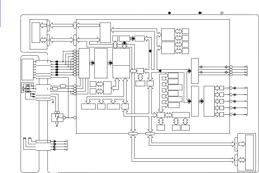
engine search manuals com.Manualslib.www from Downloaded
8-9-1
H9776BLD
DATA(VIDEO/AUDIO) SIGNAL |
|
DVD VIDEO SIGNAL |
DATA(AUDIO) SIGNAL |
|
IC503 (SDRAM) |
IC101 (MICRO CONTROLLER) |
|
22 |
|
|
|
|
|
|
|
|
|
|
|
|
|
~ |
|
217 |
|
|
|
|
|
|
|
|
|
|
|
26 |
SDRAM ADDRESS(0-11) |
SDRAM ADDRESS(0-10) |
|
|
|
|
|
|
|
|
||
|
~ |
|
|
|
|
|
|
|
|
||||
|
29 |
|
238 |
|
|
|
|
|
|
|
|
|
|
|
~ |
|
|
|
|
|
|
|
|
|
|
|
|
SDRAM |
35 |
|
|
|
EXTERNAL |
|
|
|
|
DATA |
|
|
|
|
|
|
|
|
|
|
|
RAM |
|
|
|
||
|
|
|
|
|
MEMORY |
|
|
|
DSP |
|
|
|
|
|
|
|
|
|
|
|
|
|
|
|
|
||
|
2 |
|
1 |
|
I/F |
|
|
|
|
|
|
|
|
|
|
|
|
|
|
DECODER |
INST. |
|
|
|
|||
|
|
|
|
|
DECODER |
STREAM |
|
|
|
||||
|
~ |
|
~ |
|
|
ECC |
|
|
|
|
|||
|
13 |
SDRAM DATA(0-15) |
18 |
SDRAM DATA(0-15) |
I/F |
I/F |
|
ROM |
|
|
|
||
|
42 |
252 |
|
|
|
|
|
|
|||||
|
|
|
|
|
|
|
|
|
|
|
|
||
|
~ |
|
~ |
|
|
|
|
|
|
DATA |
|
|
|
|
53 |
|
256 |
|
|
|
|
|
|
|
|
|
|
|
|
|
|
|
|
|
|
RAM |
|
|
|
||
|
|
|
|
|
|
|
|
|
I/O |
|
|
|
|
|
|
|
|
|
|
|
|
|
|
|
|
|
|
|
|
|
|
|
|
|
|
|
PROCESSOR |
INST. |
|
|
|
|
|
|
114 |
|
|
|
|
|
|
|
|
|
|
|
|
|
|
|
|
|
|
|
ROM |
|
|
|
|
|
|
|
115 |
|
|
|
|
|
|
|
|
|
|
|
|
|
|
|
|
|
|
|
|
|
|
|
|
|
|
|
116 |
|
|
|
DMA |
|
|
|
|
|
|
|
CN201 |
117 |
|
|
|
|
|
|
|
|
|
||
|
RF |
|
|
|
|
|
|
|
|
|
|||
|
C 16 |
|
132 |
DVD/CD |
|
|
|
|
|
|
|
|
|
|
|
SIGNAL |
|
|
|
|
|
|
|
|
|||
|
D 18 |
|
131 |
PROCESS |
FORMATTER |
|
|
|
|
|
|
SPDIF |
|
|
A 17 |
|
134 |
CIRCUIT |
|
|
|
|
|
|
177 |
TO DVD |
|
DETECTOR |
|
|
|
|
|
|
|
PCM-BCK |
|||||
|
|
|
|
|
|
|
|
VIDEO |
|||||
B 15 |
|
133 |
|
|
|
|
|
|
AUDIO |
170 |
|||
|
|
|
|
|
BCU |
UMAC |
|
PCM-DATA |
/AUDIO |
||||
|
E 14 |
|
129 |
|
|
|
|
171 |
|||||
|
|
|
|
|
|
|
I/F |
PCM-LRCLK |
BLOCK |
||||
|
|
|
|
|
|
|
|
||||||
|
F 12 |
|
130 |
|
|
|
|
|
SERIAL |
|
169 |
DIAGRAM |
|
|
CD/DVD 19 |
|
|
|
|
|
|
|
|
|
|
|
|
|
|
|
|
|
|
READ |
CPU |
GENERAL |
|
|
|
|
|
|
|
|
CN201 |
Q253,Q254 |
|
INST. |
|
I/O |
|
|
|
|
|
|
|
||
|
|
ROM |
|
MEMORY |
I/F |
|
|
|
|
|
|
|
|
||
CD-LD 10 |
AMP |
126 |
32BIT |
INTERRUPT |
|
|
|
|
|
|
|
||||
|
|
|
|
|
D/A |
Y |
156 |
VIDEO-Y |
|
||||||
DVD-LD |
8 AMP |
Q251,Q252 |
124 |
DATA |
CPU |
|
|
CONTROLLER |
|
|
|
||||
PD-MONI |
7 |
125 |
|
|
|
|
|
|
|
|
|
|
|
||
|
RAM |
|
|
|
TIMER |
|
|
|
C |
|
VIDEO-C |
TO DVD |
|||
GND(DVD-PD) |
6 |
|
123 |
|
|
|
|
|
|
|
|||||
|
|
|
|
|
|
|
D/A |
158 |
|||||||
|
|
|
|
|
|
|
|
|
|
VIDEO |
|||||
GND(CD-PD) |
5 |
|
|
|
|
|
|
|
|
|
|
|
|||
|
|
|
|
|
|
|
|
|
|
|
|
|
|||
|
|
|
|
|
|
WATCH DOG |
|
|
|
|
|
|
/AUDIO |
||
GND(LD) |
9 |
|
|
|
|
|
|
|
|
|
R |
|
VIDEO-R |
||
|
|
|
|
|
|
TIMER |
VIDEO |
NTSC/PAL |
D/A |
152 |
BLOCK |
||||
|
|
|
|
|
|
|
|
||||||||
|
|
|
|
|
|
|
|
|
I/F |
ENCODER |
|
|
DIAGRAM |
||
|
|
|
|
|
|
|
|
REMOTE |
|
|
|
|
|||
|
|
|
|
INTERRUPT |
WATCH DOG |
CPU |
|
|
|
|
|
|
|
|
|
|
|
|
|
|
CONTROL |
|
|
|
|
|
VIDEO-B |
|
|||
|
|
|
|
CONTROLLER |
TIMER TIMER |
I/F |
|
|
|
D/A |
B |
151 |
|
||
|
|
|
|
|
|
|
|
|
|||||||
|
1 |
3 |
|
|
|
|
|
|
|
|
D/A |
G |
149 |
VIDEO-G |
|
|
CD |
DVD |
|
|
|
|
BCU |
32BIT CPU |
|
|
|||||
|
|
|
|
|
|
|
|
|
|
|
|||||
|
83 CD/DVD |
|
|
|
|
|
|
|
|
|
|
|
|||
|
|
6 |
|
|
|
|
|
|
|
|
|
|
|
||
|
4 |
IC201 |
|
|
|
|
|
|
|
|
|
|
|
|
|
|
|
|
|
|
|
|
|
|
|
|
|
|
|
|
|
|
|
(SW) |
|
|
|
|
DEBUG |
INST |
DATA |
|
|
|
|
|
|
|
|
|
|
|
|
|
|
|
|
|
|
|
|||
|
|
|
|
|
|
|
RAM |
RAM |
|
|
|
|
|
|
|
|
|
|
|
|
|
|
|
|
|
|
|
|
|
||
|
|
|
|
|
|
192~212 |
23~51 |
|
|
|
|
|
|
IC103 (FLASH ROM) |
|
|
|
|
|
|
|
|
|
|
|
|
|
|
|
||
TS FS
|
CN201 |
|
|
1 |
|
FS(+) |
FS(+) |
|
|
~ |
|
2 |
TO DVD SYSTEM |
|
9 |
|
|
FS(-) |
FS(-) |
FADR (0-19) |
16 |
|
|
3 |
CONTROL/SERVO |
|
|||
|
TS(+) |
|
~ |
|
|
TS(+) |
1 |
BLOCK DIAGRAM |
|
25 |
|
|
TS(-) |
|
|
|
|
TS(-) |
4 |
|
|
48 |
FLASH |
|
|
|
|
|
ROM |
|
|
|
|
29 |
|
|
|
|
|
~ |
|
|
|
|
FDQ (0-15) |
36 |
|
|
|
|
38 |
|
|
|
|
|
|
|
|
|
|
|
|
~ |
|
PICK-UP |
|
|
|
45 |
|
UNIT |
DVD MAIN CBA UNIT |
|
|
|
|
Diagram Block Process Signal Digital
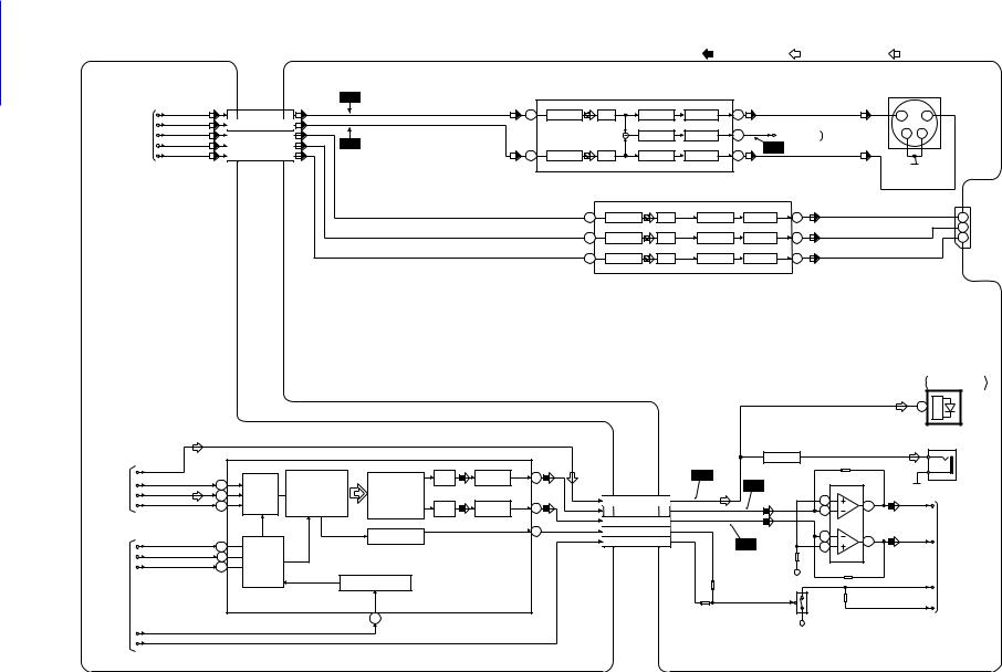
engine search manuals com.Manualslib.www from Downloaded
|
VIDEO-Y |
|
FROM DIGITAL |
VIDEO-C |
|
VIDEO-R |
||
SIGNAL PROCESS |
||
VIDEO-G |
||
BLOCK DIAGRAM |
||
|
VIDEO-B |
|
DVD VIDEO SIGNAL |
DATA(AUDIO) SIGNAL |
|
DVD AUDIO SIGNAL |
|
|
|
WF4 |
|
IC1403 (VIDEO DRIVER) |
|
|
|
|
|
|
|
|
CN601 |
|
CN1601 |
|
|
|
|
|
|
|
|
|
|
|
|
|
|
|
|
|
|
|
|
Y |
|
C |
||
1 |
VIDEO-Y |
1 |
|
3 |
4dB AMP |
LPF |
2dB AMP |
DRIVER |
5 |
|
3 |
||
|
|
|
4 |
||||||||||
10 VIDEO-C |
10 |
|
|
|
|
|
|
|
|
TO VIDEO |
1 |
2 |
|
|
|
|
|
|
|
|
|
|
6 |
|
|||
4 |
VIDEO-R |
4 |
|
|
|
-6dB |
8dB AMP |
DRIVER |
DVD-VIDEO |
BLOCK DIAGRAM |
|||
8 |
VIDEO-G |
8 |
WF5 |
|
|
|
|
|
|
WF6 |
<VCR SECTION> |
|
|
|
1 |
4dB AMP |
LPF |
2dB AMP |
DRIVER |
7 |
|
|
|
||||
6 |
VIDEO-B |
6 |
|
|
|
|
|
||||||
|
|
|
|
|
|
|
|
|
|
|
|
JK1401 |
|
|
|
|
|
|
|
|
|
|
|
|
|
S-VIDEO OUT |
|
|
IC102 (VIDEO DRIVER) |
|
|
|
JK101 |
|
|
|
|
|
|
|
|
|
|
8 |
4dB AMP |
LPF |
2dB AMP |
DRIVER |
10 |
15 |
DVD-R |
|
|
|
|
|
|
11 |
DVD-G |
6 |
4dB AMP |
LPF |
2dB AMP |
DRIVER |
11 |
7 |
DVD-B |
1 |
4dB AMP |
LPF |
2dB AMP |
DRIVER |
15 |
|
|
9-9-1
FROM
DIGITAL
SIGNAL
PROCESS
BLOCK
DIAGRAM
FROM
DVD SYSTEM CONTROL /SERVO BLOCK DIAGRAM
H9776BLVD
|
|
|
|
|
|
|
|
|
|
|
IC1204 |
|
|
|
|
|
|
|
|
|
|
|
FIBER OPTIC |
|
|
|
|
|
|
|
|
|
|
|
TRANS MODULE |
|
|
|
|
|
|
|
|
|
|
|
3 |
|
|
|
|
|
|
|
|
|
|
Q1351 |
JK1202 |
|
IC601 (AUDIO DAC) |
|
|
|
|
|
|
|
|
||
|
|
|
|
|
|
|
|
BUFFER |
DIGITAL |
||
|
|
|
|
|
|
|
|
|
|
||
SPDIF |
|
|
|
|
|
|
|
|
|
|
|
|
4X/8X |
|
|
|
L-CH |
|
|
WF9 |
|
AUDIO OUT |
|
|
|
|
|
|
|
|
|
|
|||
PCM-BCK |
|
ENPHANCED |
DAC |
LPF+AMP |
7 |
|
|
IC1201 (AMP) |
|||
|
OVERSAMPLING |
|
|
WF7 |
|||||||
1 |
SERIAL |
|
|
|
|
|
|
|
|||
PCM-DATA0 |
DIGITAL FILTER |
MULTI-LEVEL |
|
|
|
CN601 |
CN1601 |
|
|
DVD- |
|
2 |
PORT |
/FUNCTION |
DELTA-SIGMA |
|
|
|
19 SPDIF |
19 |
|
5 |
A-OUT(L) |
PCM-LRCLK |
|
|
|
R-CH |
|
||||||
3 |
|
|
MODULATOR |
|
|
|
|
|
|
7 |
|
|
CONTROLLER |
DAC |
LPF+AMP |
8 |
14 DVD-A(L) |
14 |
|
6 |
|||
|
|
|
|
||||||||
|
|
|
|
|
|
|
16 DVD-A(R) |
16 |
|
|
DVD- |
|
|
|
|
|
|
11 |
15 DVD-A(R)-MUTE 15 |
|
|
||
|
|
|
ZERO DETECT |
|
|
|
2 |
A-OUT(R) |
|||
ADAC-MD |
|
|
|
|
|
13 DVD-A-MUTE 13 |
|
||||
|
|
|
|
|
|
WF8 |
3 |
1 |
|||
13 |
|
|
|
|
|
|
|
|
TO Hi-Fi AUDIO |
||
ADAC-MC |
|
|
|
|
|
|
|
|
|
|
|
SERIAL |
|
|
|
|
|
|
|
|
|
BLOCK DIAGRAM |
|
14 |
|
|
|
|
|
|
|
|
|
||
ADAC-ML |
CONTROL |
|
|
|
|
|
|
|
|
|
<VCR SECTION> |
15 |
|
|
|
|
|
|
|
|
|
||
|
|
|
SYSTEM CLOCK |
|
|
|
|
|
|
AUDIO+5V |
A-MUTE(R) |
|
|
|
|
|
|
|
|
|
|
||
|
|
|
|
|
|
|
|
|
|
Q1204 |
A-MUTE(L) |
|
|
|
16 |
|
|
|
|
|
|
|
|
PCM-SCLK |
|
|
|
|
|
|
|
|
|
+3.3V |
|
A-MUTE |
|
|
|
|
|
|
|
|
|
|
|
|
|
|
|
|
|
|
|
|
|
|
|
DVD MAIN CBA UNIT |
MAIN CBA |
Diagram Block Audio / Video DVD

FUNCTION INDICATOR SYMBOLS
Note:
If a mechanical malfunction occurs, the power is turned off. When the power comes on again after that by pressing [FUNCTION] button, an error message is displayed on the TV screen for 5 seconds.
MODE |
INDICATOR ACTIVE |
|
|
When reel or capstan mechanism is not |
“A R” is displayed on a TV screen. (Refer to Fig. 1.) |
functioning correctly |
|
|
|
When tape loading mechanism is not func- |
“A T” is displayed on a TV screen. (Refer to Fig. 2.) |
tioning correctly |
|
|
|
When cassette loading mechanism is not |
“A C” is displayed on a TV screen. (Refer to Fig. 3.) |
functioning correctly |
|
|
|
When the drum is not working properly |
“A D” is displayed on a TV screen. (Refer to Fig. 4.) |
|
|
P-ON Power safety detection |
“A P” is displayed on a TV screen. (Refer to Fig. 5.) |
|
|
TV screen
When reel or capstan mechanism is not functioning |
When the drum is not working properly |
correctly |
|
A R |
A D |
Fig. 1 |
Fig. 4 |
When tape loading mechanism is not functioning cor- |
P-ON Power safety detection |
rectly |
|
A T |
A P |
Fig. 2 |
Fig. 5 |
When cassette loading mechanism is not functioning correctly
A C
Fig. 3
1-9-10 |
H9700FIS |
Downloaded from www.Manualslib.com manuals search engine
SCHEMATIC DIAGRAMS / CBA’S AND TEST POINTS
Standard Notes
WARNING
Many electrical and mechanical parts in this chassis have special characteristics. These characteristics often pass unnoticed and the protection afforded by them cannot necessarily be obtained by using replacement components rated for higher voltage, wattage, etc. Replacement parts that have these special safety characteristics are identified in this manual and its supplements; electrical components having such features are identified by the mark " ! " in the schematic diagram and the parts list. Before replacing any of these components, read the parts list in this manual carefully. The use of substitute replacement parts that do not have the same safety characteristics as specified in the parts list may create shock, fire, or other hazards.
Notes:
1.Do not use the part number shown on these drawings for ordering. The correct part number is shown in the parts list, and may be slightly different or amended since these drawings were prepared.
2.All resistance values are indicated in ohms (K=103, M=106).
3.Resistor wattages are 1/4W or 1/6W unless otherwise specified.
4.All capacitance values are indicated in F (P=10-6 F).
5.All voltages are DC voltages unless otherwise specified.
6.Electrical parts such as capacitors, connectors, diodes, IC’s, transistors, resistors, switches, and fuses are identified by four digits. The first two digits are not shown for each component. In each block of the diagram, there is a note such as shown below to indicate these abbreviated two digits.
1-10-1 |
SCPA1 |
Downloaded from www.Manualslib.com manuals search engine
 Loading...