


DK27..FA
DK27..FA
Fast Switching Thyristor
Replaces January 2000 version, DS4269-3.0 |
DS4269-4.0 July 2001 |
FEATURES
■Low Switching Losses At High Frequency
■Fully Characterised For Operation Up To 20kHz
APPLICATIONS
■High Power Inverters And Choppers
■UPS
■AC Motor Drives
■Induction Heating
■Cycloconverters
VOLTAGE RATINGS
Type Number |
Repetitive Peak |
Conditions |
|
Voltages |
|
|
VDRM VRRM |
|
|
V |
|
DK27 12FA K or M |
1200 |
VRSM = VRRM + 100V |
DK27 10FA K or M |
1000 |
|
|
|
IDRM = IRRM = 25mA |
|
|
at VRRM or VDRM & Tvj |
|
|
|
ORDERING INFORMATION
When ordering, select the required part number shown in the Voltage Ratings selection table, then:-
Add K to type number for 3/4" 16 UNF thread, e.g. DK27 12FAK
or
Add M to type number for M16 thread, e.g. DK27 12FAM.
Note: Please use the complete part number when ordering and quote this number in any future correspondance relating to your order.
KEY PARAMETERS
VDRM |
1200V |
|
IT(RMS) |
290A |
|
ITSM |
5000A |
|
dVdt |
200V/ |
s |
dI/dt |
500A/ |
s |
tq |
20 s |
|
Outline type code: TO93
See Package Details for further information.
Fig. 1 Package outline
1/13
www.dynexsemi.com
DK27..FA
CURRENT RATINGS
Symbol |
Parameter |
|
|
Conditions |
Max. |
Units |
|
|
|
|
|
|
|
||
I |
T(AV) |
Mean on-state current |
Half wave resistive load, T = 80oC |
185 |
A |
||
|
|
|
|
case |
|
|
|
|
|
|
|
|
|
|
|
I |
|
RMS value |
T |
case |
= 80oC |
290 |
A |
T(RMS) |
|
|
|
|
|
||
SURGE RATINGS
Symbol |
Parameter |
|
|
|
Conditions |
Max. |
Units |
|
|
|
|
|
|
|
|
|
|
I |
TSM |
Surge (non-repetitive) on-state current |
t |
p |
≥ |
10ms half sine; T = 125oC |
5.0 |
kA |
|
|
|
|
case |
|
|
||
|
|
|
|
|
|
VR = 0% VRRM - 1/4 sine |
|
|
|
I2t |
I2t for fusing |
|
|
|
125.0 x 10³ |
A2s |
|
|
|
|
|
|
|
|
|
|
THERMAL AND MECHANICAL DATA
Symbol |
Parameter |
Conditions |
Min. |
Max. |
Units |
|
|
|
|
|
|
|
|
R |
Thermal resistance - junction to case |
dc |
- |
0.13 |
oC/W |
|
th(j-c) |
|
|
|
|
|
|
|
|
|
|
|
|
|
Rth(c-h) |
Thermal resistance - case to heatsink |
Mounting torque 35.0Nm |
- |
0.06 |
oC/W |
|
|
|
with mounting compound |
|
|
|
|
|
|
|
|
|
|
|
|
|
On-state (conducting) |
- |
125 |
oC |
|
Tvj |
Virtual junction temperature |
|
|
|
|
|
Reverse (blocking) |
- |
125 |
oC |
|||
|
|
|||||
|
|
|
|
|
|
|
T |
Storage temperature range |
|
-40 |
150 |
oC |
|
stg |
|
|
|
|
|
|
|
|
|
|
|
|
|
- |
Mounting torque |
|
30.0 |
35.0 |
Nm |
|
|
|
|
|
|
|
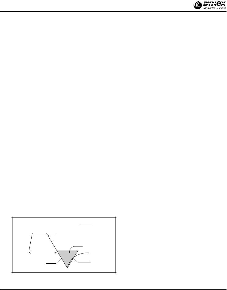
MEASUREMENT OF RECOVERED CHARGE - QRA1
Measurement of QRA1 : QRA1 = IRR x tRR
2
ITM
|
|
|
|
QRA1 |
|
|
|
|
|
|
|
|
|
|
|
|
|
|
|
|
|
|
|
|
tp |
= 1ms |
|
|
0.5x IRR |
|
|
dIR/dt |
|
||
|
|
IRR |
|
||
|
|
|
|
||
2/13
www.dynexsemi.com

DK27..FA
DYNAMIC CHARACTERISTICS
Symbol |
Parameter |
|
|
|
Conditions |
|
|
|
Min. |
Max. |
Units |
||||||
|
|
|
|
|
|
|
|
|
|
||||||||
VTM |
Maximum on-state voltage |
At 600A peak, Tcase = 25oC |
|
|
|
- |
1.85 |
V |
|
||||||||
I |
|
/I |
Peak reverse and off-state current |
At V |
|
/V |
, T |
= 125oC |
|
|
|
- |
25 |
mA |
|||
RRM |
|
DRM |
|
|
RRM DRM |
case |
|
|
|
|
|
|
|
|
|||
|
|
|
|
|
|
|
|
|
|||||||||
dV/dt |
Maximum linear rate of rise of off-state voltage |
Linear to 60% V T = 125oC, Gate open circuit |
- |
200 |
V/µ |
s |
|||||||||||
|
|
|
|
|
|
|
|
DRM |
j |
|
|
|
|
|
|
|
|
|
|
|
|
|
|
|
|
|
|
|
|
||||||
dI/dt |
Rate of rise of on-state current |
Gate source 20V, 20Ω |
Repetitive 50Hz |
- |
500 |
A/µ |
s |
||||||||||
|
|
|
|
|
|
|
|
|
|
|
|
||||||
tr < 0.5µ s, Tj |
= 125˚C |
Non-repetitive |
- |
800 |
A/µ |
s |
|||||||||||
|
|
|
|
|
|||||||||||||
|
|
|
|
|
|
|
|
|
|
|
|
|
|
|
|
||
V |
T(TO) |
Threshold voltage |
At T |
|
= 125oC |
|
|
|
|
- |
1.2 |
V |
|
||||
|
|
vj |
|
|
|
|
|
|
|
|
|
|
|||||
|
|
|
|
|
|
|
|
|
|
|
|
|
|
|
|||
|
r |
T |
On-state slope resistance |
At T |
|
= 125oC |
|
|
|
|
- |
1.0 |
mΩ |
|
|||
|
|
|
|
vj |
|
|
|
|
|
|
|
|
|
|
|||
|
|
|
|
|
|
|
|
|
|||||||||
tgd |
Delay time |
Tj = 25˚C, IT = 50A, |
|
|
|
1.5* |
- |
µ s |
|||||||||
|
|
|
|
|
VD = 300V, IG = 1A, |
|
|
|
|
|
|
|
|||||
|
|
|
|
|
|
|
|
|
|
|
|
||||||
t(ON)TOT |
Total turn-on time |
dI/dt = 30A/µ |
s, dIG/dt = 1A/µ s |
|
|
3* |
- |
µ s |
|||||||||
|
IH |
Holding current |
Tj = 25oC, ITM = 1A, VD = 12V |
|
|
|
- |
70 |
mA |
||||||||
|
|
|
|
|
|
|
|
|
|||||||||
|
tq |
Turn-off time |
Tj = 125˚C, IT = 200A, VR = 50V, |
|
t code: A |
- |
20 |
µ s |
|||||||||
|
|
|
|
|
dV/dt = 200V/µ s (Linear to 60% V |
), |
q |
|
|
|
|
||||||
|
|
|
|
|
dIR/dt = 30A/µ |
|
|
DRM |
|
|
|
|
|
||||
|
|
|
|
|
s, Gate open circuit |
|
|
|
|
|
|
||||||
|
|
|
|
|
|
|
|
|
|
|
|
|
|
|
|
|
|
*Typical value.
GATE TRIGGER CHARACTERISTICS AND RATINGS
Symbol |
Parameter |
|
|
|
|
|
|
Conditions |
Typ. |
Max. |
Units |
||||||||
|
|
|
|
|
|
|
|
|
|
|
|
|
|||||||
V |
GT |
Gate trigger voltage |
V |
|
= 12V, T |
= 25oC, R |
L |
= 6Ω |
- |
3.0 |
V |
||||||||
|
|
|
|
DRM |
|
|
|
case |
|
|
|
|
|
|
|
||||
|
|
|
|
|
|
|
|
|
|
|
|
|
|
||||||
I |
GT |
Gate trigger current |
V |
DRM |
= 12V, T |
= 25oC, R |
L |
= 6Ω |
- |
200 |
mA |
||||||||
|
|
|
|
|
|
case |
|
|
|
|
|
|
|
|
|||||
|
|
|
|
|
|
|
|
|
|
|
|
|
|
||||||
V |
GD |
Gate non-trigger voltage |
At V |
DRM |
T |
case |
= 125oC, R |
L |
= 1kΩ |
- |
0.2 |
V |
|||||||
|
|
|
|
|
|
|
|
|
|
|
|
|
|
|
|
|
|
||
VRGM |
Peak reverse gate voltage |
|
|
|
|
|
|
|
|
|
|
|
|
|
- |
5.0 |
V |
||
IFGM |
Peak forward gate current |
Anode positive with respect to cathode |
- |
4 |
A |
||||||||||||||
PGM |
Peak gate power |
|
|
|
|
|
|
|
|
|
|
|
|
|
- |
16 |
W |
||
PG(AV) |
Mean gate power |
|
|
|
|
|
|
|
|
|
|
|
|
|
- |
3.0 |
W |
||
3/13
www.dynexsemi.com

DK27..FA
CURVES
Fig.2 Maximum (limit) on-state characteristics |
Fig.3 Gate characteristics |
Fig.4 Typical recovered charge (for a device rated VDRM = 800V, tq = 20 s)
4/13
www.dynexsemi.com
 Loading...