

Ver. 1
SERVICE MANUAL
MODEL JP E3 E2 EK E2A E1C E1K EUT
DN-V210
DN-V310
33
33
DVD VIDEO PLAYER
注 意
サービスをおこなう前に、このサービスマニュアルを
必ずお読みください。本機は、火災、感電、けがなど
に対する安全性を確保するために、さまざまな配慮を
おこなっており、また法的には「電気用品安全法」に
もとづき、所定の許可を得て製造されております。
従ってサービスをおこなう際は、これらの安全性が維
持されるよう、このサービスマニュアルに記載されて
いる注意事項を必ずお守りください。
●
For purposes of improvement, specifications and
design are subject to change without notice.
●
Please use this service manual with referring to the
operating instructions without fail.
●
Some illustrations using in this service manual are
slightly different from the actual set.
PROFESSIONAL BUSINESS COMPANY
●
本機の仕様は性能改良のため、予告なく変更すること
があります。
●
補修用性能部品の保有期間は、製造打切後 8 年です。
●
修理の際は、必ず取扱説明書を参照の上、作業を行っ
てください。
●
本文中に使用しているイラストは、説明の都合上現物
と多少異なる場合があります。
TOKYO, JAPAN
X0357 V.01 DE/CDM 0707
SAFETY PRECAUTIONS
The following check should be performed for the continued protection of the customer and service technician.
LEAKAGE CURRENT CHECK
Before returning the unit to the customer, make sure you make either (1) a leakage current check or (2) a line to chassis
resistance check. If the leakage current exceeds 0.5 milliamps, or if the resistance from chassis to either side of the power
cord is less than 460 kohms, the unit is defective.
LASER RADIATION
Do not stare into beam or view directly with optical instruments, class 3A laser product.
DN-V210/DN-V310
CAUTION
Please heed the points listed below during servicing and inspection.
◎ Heed the cautions!
Spots requiring particular attention when servicing, such as
the cabinet, parts, chassis, etc., have cautions indicated on
labels or seals. Be sure to heed these cautions and the cautions indicated in the handling instructions.
◎ Caution concerning electric shock!
(1) An AC voltage is impressed on this set, so touching inter-
nal metal parts when the set is energized could cause
electric shock. Take care to avoid electric shock, by for example using an isolating transformer and gloves when
servicing while the set is energized, unplugging the power
cord when replacing parts, etc.
(2)There are high voltage parts inside. Handle with extra care
when the set is energized.
◎
Caution concerning disassembly and assembly!
Though great care is taken when manufacturing parts from
sheet metal, there may in some rare cases be burrs on the
edges of parts which could cause injury if fingers are moved
across them. Use gloves to protect your hands.
◎ Only use designated parts!
The set's parts have specific safety properties (fire resistance, voltage resistance, etc.). For replacement parts, be
sure to use parts which have the same properties. In particular, for the important safety parts that are marked ! on wiring
diagrams and parts lists, be sure to use the designated parts.
◎ Be sure to mount parts and arrange the
wires as they were originally!
For safety reasons, some parts use tape, tubes or other insulating materials, and some parts are mounted away from the
surface of printed circuit boards. Care is also taken with the
positions of the wires inside and clamps are used to keep
wires away from heating and high voltage parts, so be sure to
set everything back as it was originally.
◎ Inspect for safety after servicing!
Check that all screws, parts and wires removed or disconnected for servicing have been put back in their original positions, inspect that no parts around the area that has been
serviced have been negatively affected, conduct an insulation
check on the external metal connectors and between the
blades of the power plug, and otherwise check that safety is
ensured.
(Insulation check procedure)
Unplug the power cord from the power outlet, disconnect the
antenna, plugs, etc., and turn the power switch on. Using a
500V insulation resistance tester, check that the insulation resistance between the terminals of the power plug and the externally exposed metal parts (antenna terminal, headphones
terminal, microphone terminal, input terminal, etc.) is 1MΩ or
greater. If it is less, the set must be inspected and repaired.
CAUTION
Many of the electric and structural parts used in the set have
special safety properties. In most cases these properties are
difficult to distinguish by sight, and using replacement parts
with higher ratings (rated power and withstand voltage) does
not necessarily guarantee that safety performance will be preserved. Parts with safety properties are indicated as shown
below on the wiring diagrams and parts lists is this service
manual. Be sure to replace them with parts with the designated part number.
(1) Schematic diagrams ... Indicated by the ! mark.
(2) Parts lists ... Indicated by the ! mark.
Concerning important safety parts
Using parts other than the designated parts
could result in electric shock, fires or other
dangerous situations.
注 意
サービス、点検時にはつぎのことにご注意願います。
◎注意事項をお守りください!
サービスのとき特に注意を必要とする個所についてはキャ
ビネット、部品、シャーシなどにラベルや捺印で注意事項を
表示しています。これらの注意書きおよび取扱説明書などの
注意事項を必ずお守りください。
◎感電に注意!
(1) このセットは、交流電圧が印加されていますので通電時
に内部金属部に触れると感電することがあります。従っ
て通電サービス時には、絶縁トランスの使用や手袋の着
用、部品交換には、電源プラグを抜くなどして感電にご
注意ください。
(2) 内部には高電圧の部分がありますので、通電時の取扱に
は十分ご注意ください。
◎分解、組み立て作業時のご注意!
板金部品の端面の『バリ』は、部品製造時に充分管理をして
おりますが、板金端面は鋭利となっている箇所が有りますの
で、部品端面に触れたまま指を動かすとまれに怪我をする場
合がありますので十分注意して作業して下さい。手の保護の
ために手袋を着用してください。
◎指定部品の使用!
セットの部品は難燃性や耐電圧など安全上の特性を持った
ものとなっています。従って交換部品は、使用されていたも
のと同じ特性の部品を使用してください。特に配線図、部品
表に!印で指定されている安全上重要な部品は必ず指定の
ものをご使用ください。
◎部品の取付けや配線の引きまわしは、
元どおりに!
安全上、テープやチューブなどの絶縁材料を使用したり、プ
リント基板から浮かして取付けた部品があります。また内部
配線は引きまわしやクランパーによって発熱部品や高圧部
品に接近しないように配慮されていますので、これらは必ず
元どおりにしてください。
◎サービス後は安全点検を!
サービスのために取り外したねじ、部品、配線などが元どお
りになっているか、またサービスした個所の周辺を劣化させ
てしまったところがないかなどを点検し、外部金属端子部
と、電源プラグの刃の間の絶縁チェックをおこなうなど、安
全性が確保されていることを確認してください。
(絶縁チェックの方法)
電源コンセントから電源プラグを抜き、アンテナやプラグな
どを外し、電源スイッチを入れます。500V 絶縁抵抗計を用
いて、電源プラグのそれぞれの端子と外部露出金属部[アン
テナ端子、ヘッドホン端子、マイク端子、入力端子など]と
の間で、絶縁抵抗値が1 MΩ 以上であることを確認してく
ださい。この値以下のときはセットの点検修理が必要です。
注 意
本機に使用している多くの電気部品、および機構部品は安全
上、特別な特性を持っています。この特性はほとんどの場合、
外観では判別つきにくく、またもとの部品より高い定格(定
格電力、耐圧)を持ったものを使用しても安全性が維持され
るとは、限りません。安全上の特性を持った部品は、この
サービスマニュアルの配線図、部品表につぎのように表示し
ていますので必ず指定されている部品番号のものを使用願
います。
(1) 配線図…!マークで表示しています。
(2) 部品表…!マークで表示しています。
安全上重要な部品について
指定された部品と異なるものを使用した場合に
は、感電、火災などの危険を生じる恐れがあり
ます。
2
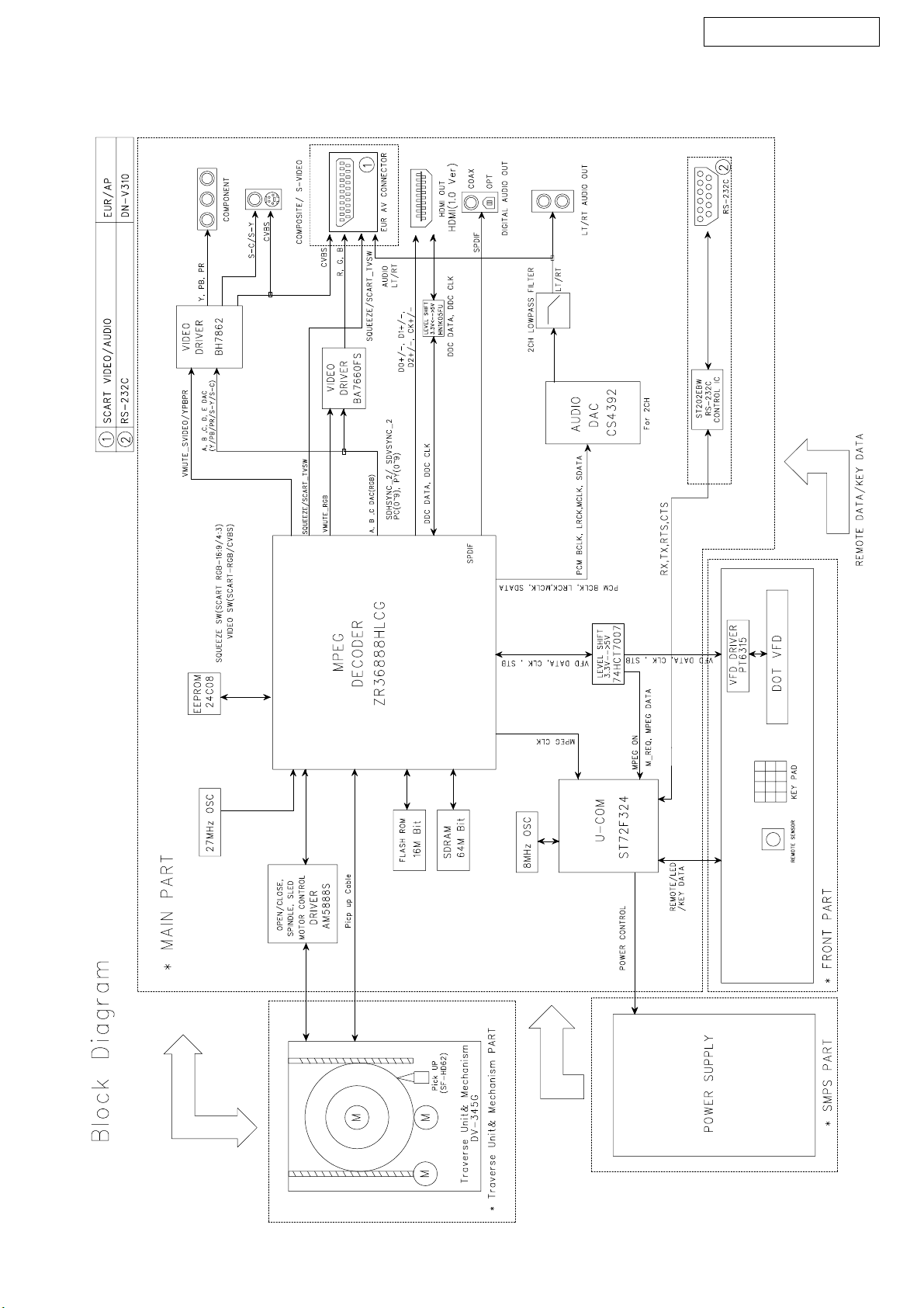
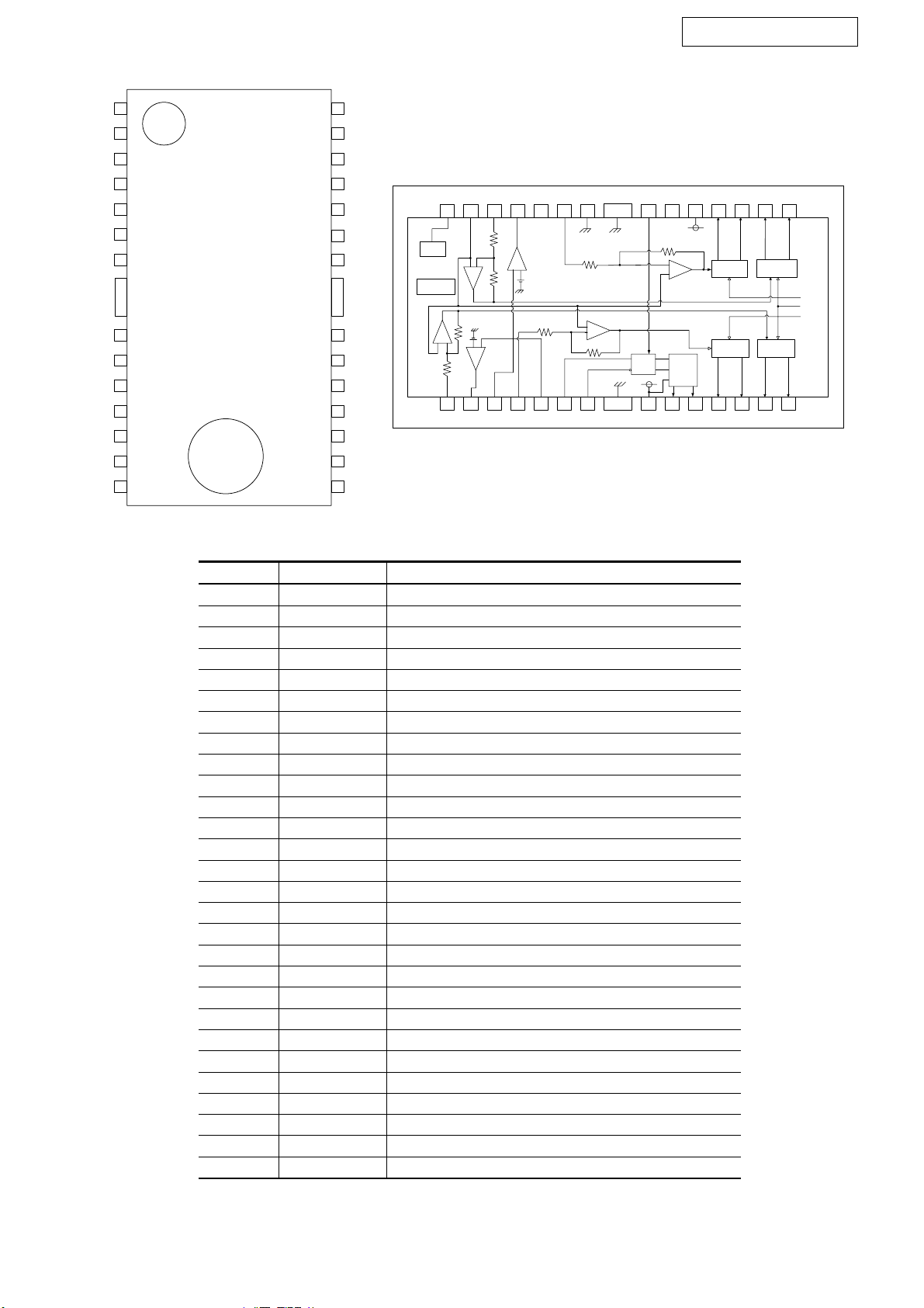
BLOCK DIAGRAM
DN-V210/DN-V310
3
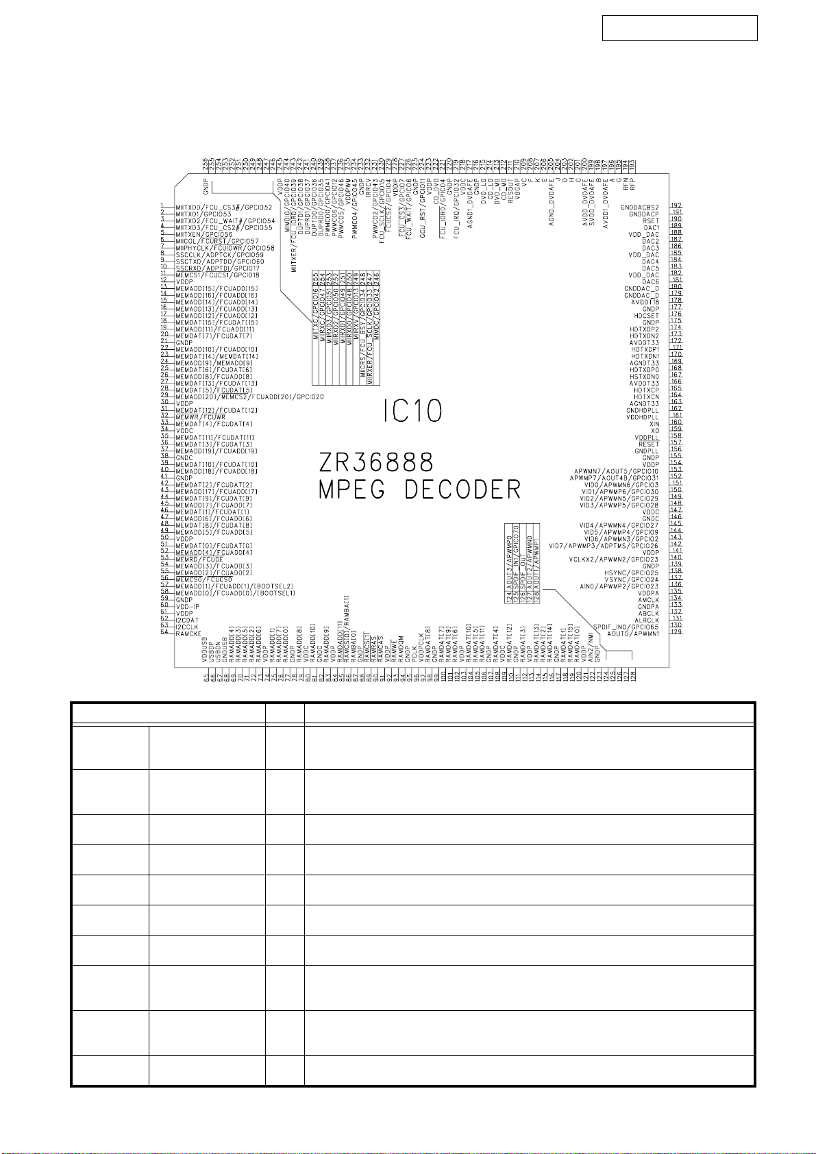
SEMICONDUCTORS
Only major semiconductors are shown, general semiconductors etc. are omitted to list.
主な半導体を記載しています。汎用の半導体は記載を省略しています。
● IC's
ZR36888HLCG (IC10)
DN-V210/DN-V310
Pin Functions Dir. Description
1 GPCI/O[52] I/O General purpose input/output, monitored/controlled by the CPU or DSP SW
DVDVALID I AV data valid input for FE by-pass. Programmable polarity
FCUIF[35] O Flash card interface unit output signal
2 GPCI/O[53] I/O General purpose input/output, monitored/controlled by the CPU or DSP SW
DVDSOS I AV start of sector indication input for FE by-pass. Programmable polarity
AOUT[4] O Serial output of digital stereo audio
3 GPCI/O[54] I/O General purpose input/output, monitored/controlled by the CPU or DSP SW
FCUIF[30] I/O Flash card interface unit input/output signal
4 GPCI/O[55] I/O General purpose input/output, monitored/controlled by the CPU or DSP SW
FCUIF[31] I/O Flash card interface unit input/output signal
5 GPCI/O[56] I/O General purpose input/output, monitored/controlled by the CPU or DSP SW
DVDREQ O AV data request output for FE by-pass. Programmable polarity
6 GPCI/O[57] I/O General purpose input/output, monitored/controlled by the CPU or DSP SW
FCUIF[36] I/O Flash card interface unit input/output signal
7 GPCI/O[58] I/O General purpose input/output, monitored/controlled by the CPU or DSP SW
FCUIF[33] I/O Flash card interface unit input/output signal
8 SSCCLK I SSC clock input signal
GPCI/O[59] I/O General purpose input/output, monitored/controlled by the CPU or V8 SW
FGPCI/O[4] I/O General purpose input/output, monitored/controlled by the V8 SW
9 SSCTXD O SSC data output signal
GPCI/O[60] I/O General purpose input/output, monitored/controlled by the CPU or V8 SW
FGPCI/O[5] I/O General purpose input/output, monitored/controlled by the V8 SW
10 SSCRXD I SSC data input
GPCI/O[17] I/O General purpose input/output, monitored/controlled by the CPU or DSP or V8 SW
4
Pin Functions Dir. Description
FGPCI/O[0] I/O General purpose input/output, monitored/controlled by the V8 SW
PM[5] O Probe mux data output
11 MEMCS[1]# O PNVM/SRAM chip select (active low) output
GPCI/O[18] I/O General purpose input/output, monitored/controlled by the CPU or DSP SW
FCUIF[29] O Flash card interface unit output signal
MEMLSB O PNVM/SRAM address I.s. byte select output
12 VDDP S 3.3 V Digital periphery power supply
13, 14 MEMAD[15,16] O PNVM/SRAM address bus outputs
FCUIF[45,46] O Flash card interface unit output signal
SYSIND[1,0] I General purpose system configuration indication input. Level sampled during RESET
15 MEMAD[14] O PNVM/SRAM address bus output
FCUIF[44] O Flash card interface unit output signal
PLLUBYP I PLLu by-pass selection input. Level sampled during RESET. In normal operation the pin
must be low during RESET
16 MEMAD[13] O PNVM/SRAM address bus output
FCUIF[43] O Flash card interface unit output signal
17 MEMAD[12] O PNVM/SRAM address bus output
FCUIF[42] O Flash card interface unit output signal
PHSPLLBYP I Processing HS PLL by-pass selection input. Level sampled during RESET. In normal oper-
ation the pin must be low during RESET
18 MEMAD[15] I/O PNVM/SRAM bi-directional data bus
FCUIF[28] I/O Flash card interface unit input/output signal
19 MEMAD[11] O PNVM/SRAM address bus output
FCUIF[41] O Flash card interface unit output signal
PDIV2BYP I PDIV2 by-pass selection input. Level sampled during RESET. In normal operation the pin
must be low during RESET
20 MEMDA[7] I/O PNVM/SRAM bi-directional data bus
FCUIF[9] I/O Flash card interface unit input/output signals
21 GNDP S Digital periphery ground of 3.3 V supply
22 MEMAD[10] O PNVM/SRAM address bus output
FCUIF[20] O Flash card interface unit output signal
TESTMODE I Operational mode selection. Level sampled during RESET. In normal operation the pin
must be low during RESET
23 MEMAD[14] I/O PNVM/SRAM bi-directional data bus
FCUIF[27] I/O Flash card interface unit input/output signal
24 MEMAD[9] O PNVM/SRAM address bus output
FCUIF[19] O Flash card interface unit output signal
PLLEBYP I PLLe by-pass selection input. Level sampled during RESET. In normal operation the pin
must be low during RESET
25 MEMAD[6] I/O PNVM/SRAM bi-directional data bus
FCUIF[8] I/O Flash card interface unit input/output signal
26 MEMAD[8] O PNVM/SRAM address bus output
FCUIF[18] O Flash card interface unit output signal
27 MEMAD[13] I/O PNVM/SRAM bi-directional data bus
FCUIF[26] I/O Flash card interface unit input/output signal
28 MEMAD[5] I/O PNVM/SRAM bi-directional data bus
FCUIF[7] I/O Flash card interface unit input/output signal
29 MEDAD[20] O PNVM/SRAM address bus output
MEMCS[2]# O PNVM/SRAM chip select (active low) output
GPCI/O[19] I/O General purpose input/output, monitored/controlled by the CPU or DSP SW
FCUIF[50] O Flash card interface unit output signal
MEMMSB O PNVM/SRAM address m.s. byte select output
30 VDDP S 3.3 V Digital periphery power supply
31 MEMAD[12] I/O PNVM/SRAM bi-directional data bus
FCUIF[25] I/O Flash card interface unit input/output signal
32 MEMWR# O PNVM/SRAM write enable (active low) output
FCUIF[0] O Flash card interface unit output signal
33 MEMAD[4] I/O PNVM/SRAM bi-directional data bus
FCUIF[6] I/O Flash card interface unit input/output signal
34 VDDC S 1.8 V Digital core power supply
35 MEMAD[11] I/O PNVM/SRAM bi-directional data bus
FCUIF[24] I/O Flash card interface unit input/output signals
36 MEMAD[3] O PNVM/SRAM bi-directional data bus
FCUIF[5] O Flash card interface unit output signal
37 MEMAD[19] O PNVM/SRAM address bus output
FCUIF[49] O Flash card interface unit output signal
DN-V210/DN-V310
5
Pin Functions Dir. Description
PLLABYP I PLLA by-pass selection input. Level sampled during RESET. In normal operation the pin
must be low during RESET
38 GNDC S Digital core ground of 1.8 V supply
39 MEMAD[10] I/O PNVM/SRAM bi-directional data bus
FCUIF[23] I/O Flash card interface unit input/output signal
40 MEMAD[18] O PNVM/SRAM address bus output
FCUIF[48] O Flash card interface unit output signal
BYTEMODE I Byte access mode selection input. Level sampled during RESET
41 GNDP S Digital periphery ground of 3.3 V supply
42 MEMAD[2] I/O PNVM/SRAM bi-directional data bus
FCUIF[4] I/O Flash card interface unit input/output signal
43 MEMAD[17] O PNVM/SRAM address bus output
FCUIF[47] O Flash card interface unit output signal
SYSIND[2] I General purpose system configuration indication input. Level sampled during RESET
44 MEMDA[9] I/O PNVM/SRAM bi-directional data bus
MEMAD[21] O PNVM/SRAM address bus output
FCUIF[22] I/O Flash card interface unit input/output signal
45 MEMAD[7] O PNVM/SRAM address bus output
FCUIF[17] O Flash card interface unit output signal
FLASHCFG I External flash memory configuration indication input. Level sampled during RESET
46 MEMDA[1] I/O PNVM/SRAM bi-directional data bus
FCUIF[3] I/O Flash card interface unit input/output signal
47 MEMAD[6] O PNVM/SRAM address bus output
FCUIF[16] O Flash card interface unit output signal
48 MEMDA[8] I/O PNVM/SRAM bi-directional data bus
MEMAD[20] O PNVM/SRAM address bus output
FCUIF[21] I/O Flash card interface unit input/output signal
49 MEMAD[5] O PNVM/SRAM address bus output
FCUIF[15] O Flash card interface unit output signal
50 VDDP S 3.3 V Digital periphery power supply
51 MEMDA[0] I/O PNVM/SRAM bi-directional data bus
FCUIF[2] I/O Flash card interface unit input/output signal
52 MEMAD[4] I/O PNVM/SRAM address bus output
FCUIF[14] O Flash card interface unit output signal
53 MEMRD# O PNVM/SRAM read enable (active low) output
FCUIF[1] O Flash card interface unit output signal
54, 55 MEMAD[3,2] O PNVM/SRAM address bus output
FCUIF[13,12] O Flash card interface unit output signal
56 MEMCS[0]# O PNVM/SRAM chip select (active low) output
FCUIF[38] O Flash card interface unit output signal
57,58 MEMAD[1,0] O PNVM/SRAM address bus output
FCUIF[11,10] O Flash card interface unit output signal
BOOTSEL[2,1] I CPU SW boot (and execute) source selection. Levels sampled during RESET
59 GNDP S Digital periphery ground of 3.3 V supply
60 VDD-IP S 3.3 V periphery reference voltage
61 VDDP S 3.3 V Digital periphery power supply
62 GPCI/O[61] I/O General purpose input/output, monitored/controlled by the CPU or V8 SW
FGPCI/O[6] I/O General purpose input/output, monitored/controlled by the CPU or V8 SW
63 FGPCI/O[62] I/O General purpose input/output, monitored/controlled by the CPU or V8 SW
FGPCI/O[7] I/O General purpose input/output, monitored/controlled by the V8 SW
64 RAMCKE O Clock enable signal to the SDRAM (for power down)
GPCI/O[63] I/O General purpose input/output, monitored/controlled by the CPU or DSP SW
65 VDDUSB S 3.3 V USB power supply
66 USBDP I/O USB data positive signal
67 USBDN I/O USB data negative signal
68 GNDUSB S Ground for USB 3.3 V supply
69-73 RAMADD[4,3,5,2,6] O SDRAM address bus output
74 VDDP S 3.3 V Digital periphery power supply
75-77 RAMADD[1,7,0] O SDRAM address bus output
78 GNDP S Digital periphery ground of 3.3 V supply
79 RAMADD[8] O SDRAM address bus output
80 VDDC S 1.8 V Digital core power supply
81 RAMADD[10] O SDRAM address bus output
82 GNDC S Digital core ground of 1.8 V supply
83 RAMADD[9] O SDRAM address bus output
84 VDDP S 3.3 V Digital periphery power supply
85 RAMADD[11] O SDRAM address bus output
DN-V210/DN-V310
6
DN-V210/DN-V310
Pin Functions Dir. Description
86 RAMCS[0]# O SDRAM chip select (active low)
RAMBA[1] O SDRAM bank select output
87 RAMBA[0] O SDRAM bank select output
88 GNDP S Digital periphery ground of 3.3 V supply
89 RAMCS[1]# O SDRAM chip select (active low) output
90 RAMRAS# O SDRAM row select (active low) output
91 RAMCAS# O SDRAM column select (active low) output
92 VDDP S 3.3 V Digital periphery power supply
93 RAMWE# O SDRAM write enable (active low) output
94 RAMDQM O SDRAM data masking (active high) output
95 GNDPCLK S Digital ground of filtered 3.3 V supply for PCLK
96 PCLK O SDRAM clock output (same as internal processing clock)
97 VDDPCLK S 3.3 V filtered digital power supply for PCLK
98 RAMDAT[8] I/O SDRAM bi-directional data bus
99 GNDP S Digital periphery ground of 3.3 V supply
100-102 RAMDAT[7,9,6,] I/O SDRAM bi-directional data bus
103 VDDP S 3.3 V Digital periphery power supply
104-106 RAMDAT[10,5,11] I/O SDRAM bi-directional data bus
107 GNDP S Digital periphery ground of 3.3 V supply
108 RAMDAT[4] I/O SDRAM bi-directional data bus
109 VDDC S 1.8 V Digital core power supply
110 RAMDAT[12] I/O SDRAM bi-directional data bus
111 GNDC S Digital core ground of 1.8 V supply
112 RAMDAT[3] I/O SDRAM bi-directional data bus
113 VDDP S 3.3 V Digital periphery power supply
114-116 RAMDAT[13,2,14] I/O SDRAM bi-directional data bus
117 GNDP S Digital periphery ground of 3.3 V supply
118-120 RAMDAT[1,15,0] I/O SDRAM bi-directional data bus
121 VDDP S 3.3 V Digital periphery power supply
122 GPCI/O[20] I/O General purpose input/output, monitored/controlled by the CPU or DSP SW
CPUNMI I CPU non-maskable interrupt input
RAMCKE O Clock enable signal to the SDRAM (for power down)
AIN[4] I Serial output of digital stereo audio
PM[0] O Probe mux data output
123 GNDP S Digital periphery ground of 3.3 V supply
124 ICGPCI/O[0] I/O General purpose input/output, monitored/controlled by the CPU or DSP SW. When input,
the pin can be used as general purpose external interrupt to the CPU
AOUT[3] O Serial output of digital stereo audio
ADPWMP[0] O Class D audio channel 0 output, positive signal
ADPWMP[6] O Class D audio channel 6 output, positive signal
PM[1] O Probe mux data output
125 IDGPCI/O[0] I/O General purpose input/output, monitored/controlled by the CPU or DSP SW. When input,
the pin can be used as general purpose external interrupt to the DSP
S/PDIFIN[5] I S/PDIF receiver input for detail coded or reconstructed audio data
ADPWMP[6] O Class D audio channel 6 output, negative signal
PM[2] O Probe mux data output
126 GPCI/O[64] I/O General purpose input/output, monitored/controlled by the CPU or DSP SW
S/PDIFOUT O S/PDIF transmitter output for detail coded or reconstructed audio data
ADPWMP[5] O Class D audio channel 5 output, positive signal
PM[3] O Probe mux data output
127 ADPWMN[5] O Class D audio channel 5 output, negative signal
ADPWMN[0] O Class D audio channel 0 output, negative signal
GPCI/O[21] I/O General purpose input/output, monitored/controlled by the CPU or DSP SW
AOUT[2] O Serial output of digital stereo audio
PM[4] O Probe mux data output
128 ADPWMN[4] O Class D audio channel 4 output, positive signal
ADPWMN[1] O Class D audio channel 1 output, positive signal
GPCI/O[22] I/O General purpose input/output, monitored/controlled by the CPU or DSP SW.
AOUT[1] O Serial output of digital stereo audio
PM[5] O Probe mux data output
129 AOUT[0] O Serial output of digital stereo audio
ADPWMN[1] O Class D audio channel 0 output, negative signal
130 GPAI/O I/O General purpose input/output, monitored/controlled by the ADP SW.
AOUT[3] O Serial output of digital stereo audio
GPCI/O[65] I/O General purpose input/output, monitored/controlled by the CPU SW.
S/PDIFIN[1] I S/PDIF receiver input for detail coded or reconstructed audio data
AIN[2] I Serial input of digital stereo audio
7
DN-V210/DN-V310
Pin Functions Dir. Description
ADPWMN[2] O Class D audio channel 2 output, negative signal
PM[7] O Probe mux data output
131 ALRCLK O Digital audio left/right select output for the audio port. Square wave, at the sampling fre-
quency. Programmable polarity
GPCI/O[66] I/O General purpose input/output, monitored/controlled by the CPU or DSP SW
AUTO[4] O Serial outputs of digital stereo audio
132 ABCLK O Digital audio bit-clock output. Data on AOUT and AIN is output or latched, respectively, with
the rising or falling (programmable) edge of this clock
GPCI/O[67] I/O General purpose input/output, monitored/controlled by the CPU or DSP SW
133 GNDP-A2 S Digital ground of filtered 3.3 V supply for AMCLK
134 AMCLK I/O Audio Master Clock input/output. 128, 192, 256 or 384 times the sampling frequency (pro-
135 VDDP-A2 S 3.3V filtered digital power supply for AMCLK
136 AIN[1] I Serial input of digital stereo audio
GPCI/O[23] I/O General purpose input/output, monitored/controlled by the CPU or DSP SW
ADPWMP[2] O Class D audio channel 2 output, positive signal
PM[8] O Probe mux data output
137 VSYNC# O SD digital video vertical sync output signal
HDFI I HD digital video index signal
GPCI/O[24] I/O General purpose input/output, monitored/controlled by the CPU or DSP SW
DACTEST[9] I DACs rest input
PM[9] O Probe mux data output
138 HSYNC# O SD digital video horizontal sync output signal
HDHS I HD digital video horizontal sync output signal
GPCI/O[25] I/O General purpose input/output, monitored/controlled by the CPU or DSP SW
DACTEST[8] I DACs rest input
PM[10] O Probe mux data output
139 GNDP S Digital periphery ground of 3.3 V supply
140 VCLKx2 I/O Digital video clock input/output. 27 MHz (for SD interlaced) or 54 MHz (for SD progressive)
COSYNC O Composite sync output. Active only when component analog output is selected
ICGPCI/O[1] I/O General purpose input/output, monitored/controlled by the CPU or DSP SW. When input,
ADPWMN[2] O Class D audio channel 2 output, negative signal
DACTEST[10] I DACs rest input
PM[11] O Probe mux data output
141 VDDP S 3.3 V Digital periphery power supply
142 VID[7] O Digital 4:2:2 video luma/chroma input/output, interleaved U, Y, V, Y
GPCI/O[26] I/O General purpose input/output, monitored/controlled by the CPU or DSP SW
ADPWMP[3] O Class D audio channel 3 output, positive signal
DACTEST[7] I DACs rest input
143 VID[6] I/O Digital 4:2:2 video luma/chroma input/output, interleaved U, Y, V, Y
ICGPCI/O[2] I/O General purpose input/output, monitored/controlled by the CPU or DSP SW. When input,
ADPWMN[3] O Class D audio channel 3 output, negative signal
DACTEST[6] I DACs rest input
144 VID[5] I/O Digital 4:2:2 video luma/chroma input/output, interleaved U, Y, V, Y
IDGPCI/O[1] I/O General purpose input/output, monitored/controlled by the CPU or DSP SW. When input,
ADPWMN[4] O Class D audio channel 4 output, negative signal
DACTEST[5] I DACs rest input
145 VID[4] I/O Digital 4:2:2 video luma/chroma input/output, interleaved U, Y, V, Y
GPCI/O[27] I/O General purpose input/output, monitored/controlled by the CPU or DSP SW
ADPWMN[4] O Class D audio channel 4 output, negative signal
DACTEST[4] I DACs rest input
- GNDP S Digital periphery ground of 3.3 V supply
146 GNDC S Digital core ground of 1.8 V supply
147 VDDC S 1.8 V Digital core power supply
- VDDP S 3.3 V Digital periphery supply
148 VID[3] I/O Digital 4:2:2 video luma/chroma input/output, interleaved U, Y, V, Y
GPCI/O[28] I/O General purpose input/output, monitored/controlled by the CPU or DSP SW
ADPWMN[5] O Class D audio channel 5 output, negative signal
DACTEST[3] I DACs rest input
PM[6] O Probe mux data output
149 VID[2] I/O Digital 4:2:2 video luma/chroma input/output, interleaved U, Y, V, Y
GPCI/O[29] I/O General purpose input/output, monitored/controlled by the CPU or DSP SW
ADPWMN[5] O Class D audio channel 5 output, negative signal
DACTEST[2] I DACs rest input
grammable)
or 135 MHz (for HD to external 177, output only)
the pin can be used as general purpose external interrupt to the CPU
the pin can be used as general purpose external interrupt to the CPU
the pin can be used as general purpose external interrupt to the DSP
8
DN-V210/DN-V310
Pin Functions Dir. Description
PM[12] O Probe mux data output
150 VID[1] I/O Digital 4:2:2 video luma/chroma input/output, interleaved U, Y, V, Y
GPCI/O[30] I/O General purpose input/output, monitored/controlled by the CPU or DSP SW
ADPWMN[6] O Class D audio channel 6 output, positive signal
DACTEST[1] I DACs rest input
PM[13] O Probe mux data output
151 VID[0] I/O Digital 4:2:2 video luma/chroma input/output, interleaved U, Y, V, Y
ICGPCI/O[3] I/O General purpose input/output, monitored/controlled by the CPU or DSP SW. When input,
the pin can be used as general purpose external interrupt to the CPU
ADPWMN[6] O Class D audio channel 6 output, negative signal
DACTEST[0] I DACs rest input
PM[14] O Probe mux data output
152 GPCI/O[31] I/O General purpose input/output, monitored/controlled by the CPU or DSP SW
ADPWMN[7] O Class D audio channel 7 output, positive signal
AOUT[4] O Serial output of digital stereo audio
PMCLK O Probe mux data output
153 IDGPCI/O[2] I/O General purpose input/output, monitored/controlled by the CPU or DSP SW. When input,
the pin can be used as general purpose external interrupt to the DSP
AOUT[5] O Serial output of digital stereo audio
ADPWMN[7] O Class D audio channel 7 output, negative signal
154 VDDP S 3.3 V Digital periphery power supply
155 GNDP S Digital periphery ground of 3.3 V supply
156 GNDA S Ground plane of internal PLL circuit
157 RESET# ID Reset input (active low)
158 VDDA S 1.8 V Power supply for internal PLL circuit
159 XO AO Output to a crystal that is connected to GCLKP. If a crystal is not used at GCLKP, XO must
160 GCLKP ID 27.000MHz clock generator or crystal input for the PLL
161 AHVDD S 1.8 V Power supply for the HD PLL
162 AHGND S Ground for the 1.8V HD PLL power supply
163 AGNDP S Ground for the 3.3V HD unit power supply
164 HDTXCN O HDMI clock negative output signal
165 HDTXCP O HDMI clock positive output signal
166 AVDDP S 3.3V Power supply for the HD unit
167 HDTXDN0 O HDMI data channel 0 negative output signal
168 HDTXDP0 O HDMI data channel 0 positive output signal
169 AGNDP S Ground for the 3.3V HD unit power supply
170 HDTXDN1 O HDMI data channel 1 negative output signal
171 HDTXDP1 O HDMI data channel 1 positive output signal
172 AVDDP S 3.3V Power supply for the HD unit
173 HDTXDN2 O HDMI data channel 2 negative output signal
174 HDTXDP2 O HDMI data channel 2 positive output signal
175 AGNDP S Ground for the 3.3V HD unit power supply
176 HDCSET AI/O Resistive load for output current setting
177 AGNDC S Ground for 1.8V HD unit power supply
179, 180 GNDDACD S Ground for the video DACs 3.3 V analog power supply
181 CVBS (DAC 6) Analog CVBS (SD only) video output
182 VDDDACD S Ground for video DACs 3.3 V analog power supply
183 CVBS/C/Y (DAC 5) AO Analog video output that can be selected to be CVBS (SD only), C (SD only) or Y (SD only).
184 CVBS/G/Y (DAC 4) AO Analog video output that can be selected to be CVBS (SD only), or G/Y (SD or HD). The
185 VDDDAC S 3.3 V Analog power supply for the video DACs
186 CVBS/C/Y (DAC 3) AO Analog video output that can be selected to be CVBS (SD only), C (SD only) or Y (SD only).
187 Y/R/V/C (DAC 2) AO Analog video output that can be selected to be Y (SD only), or R/V (SD or HD) or C (SD
188 VDDDAC S 3.3 V Analog power supply for the video DACs
189 C/B/U (DAC 1) AO Analog video output that can be selected to be C (SD only), or B/U (SD or HD). The selec-
190 RSET AI/O Resistive load for gain adjustment of the DACs
191 GNDDACP S Ground for the video DACs 3.3 V analog power supply
192 GNDDABS2 S Common Ground for the video and SERVO DACs
193 RFINP AI RF positive input signal (differential input) // RF input signal (single ended)
194 RFINN AI RF negative input signal (differential input) // RF reference input signal
be left not connected
The selection is independent the specific selection of the other four DACs
selection is independent of the specific selection of the other four DACs. The selection
between G and Y depends also on DACs 1 and 2 selections
The selection is independent of the specific selection of the other four DACs
only). The selection is independent of the specific selection of the other four DACs. The
selection between R and V depends also on DACs 1 and 4 selections
tion is independent of the specific selection of the other four DACs. The selection between
B and U depends also on DACs 2 and 4 selections
9
DN-V210/DN-V310
Pin Functions Dir. Description
195 ADCIN[G] AI ADC input signal (e.g. from OPU)
196 ADCIN[A] AI ADC input signal (e.g. from OPU)
197 VDDAFE S Analog AFE 3.3 V supply
198 ADCIN[B] AI ADC input signal (e.g. from OPU)
199 VDDSAFE S Analog AFE 3.3 V supply shield
200 VDDAFE S Analog AFE 3.3 V supply
201 ADCIN[C] AI ADC input signal (e.g. from OPU)
202 ADCIN[H] AI ADC input signal (e.g. from OPU)
203, 204 ADCIN[D,J] AI ADC input signals (e.g. from OPU)
205 GNDADC S Analog ADC (AFE) ground of 3.3 V supply
206-208 ADCIN[E,K,F] AI ADC input signals (e.g. from OPU)
209 OPUREF AO OPU reference voltage output
210 BGCAP AI/O Capacitive load for internal band-gap voltage generation
211 RESLOAD AI/O Resistive load for internal reference voltage generation
212 CDMD AI CD LASER monitor diode input
213 DVDMD AI DVD LASER monitor diode input
214 CDLD AO CD LASER diode drive output
215 DVDLD AO DVD LASER diode drive output
216 GNDAFER AI AFE analog reference voltage ground
217 GNDADC S Analog ADC (AFE) ground of 3.3 V supply
218 VDDC S 1.8 V Digital core power supply
219 GPCI/O[32] I/O General purpose input/output, monitored/controlled by the CPU or DSP SW
FCUIF[32] I/O Flash card interface unit output signal
220 GNDC S Digital core ground of 1.8 V supply
221 ICGPCI/O[4] I/O General purpose input/output, monitored/controlled by the CPU or DSP SW. When input,
FCUIF[37] O Flash card interface unit output signal
S/PDIFIN[4] I S/PDIF receiver input for detail coded or reconstructed audio data
222 ICGPCI/O[5] I/O General purpose input/output, monitored/controlled by the CPU or DSP SW. When input,
FCUIF[33] O Flash card interface unit output signal
S/PDIFIN[2] I S/PDIF receiver input for detail coded or reconstructed audio data
223 VDDP S 3.3 V Digital periphery power supply
224 IDGPCI/O[3] I/O General purpose input/output, monitored/controlled by the CPU or DSP SW. When input,
FCUIF[36] I/O Flash card interface unit input/output signal
225 GNDP S Digital periphery ground of 3.3 V supply
226 ICGPCI/O[6] I/O General purpose input/output, monitored/controlled by the CPU or DSP SW. When input,
FCUIF[30] I/O Flash card interface unit input/output signal
227 ICGPCI/O[7] I/O General purpose input/output, monitored/controlled by the CPU or DSP SW. When input,
FCUIF[35] I/O Flash card interface unit input/output signal
228 VDD-IP S 3.3 V periphery reference voltage
229 ICGPCI/O[6] I/O General purpose input/output, monitored/controlled by the CPU or DSP SW. When input,
FCUIF[31] I/O Flash card interface unit input/output signal
NRZCLK I NZR clock input for AFE and DRC by-pass
230 IDGPCI/O[7] I/O General purpose input/output, monitored/controlled by the CPU or DSP SW. When input,
FCUIF[34] I/O Flash card interface unit input/output signal
S/PDIFOUT O S/PDIF output for detail coded or reconstructed audio data
231 PWMCO[2] O PWM4 output signal
GPCI/O[43] I/O General purpose input/output, monitored/controlled by the CPU or DSP SW
232 PWMCO[3] O PWM5 output signal
GPCI/O[44] I/O General purpose input/output, monitored/controlled by the CPU or DSP or V8 SW
FGPCI/O[1] I/O General purpose input/output, monitored/controlled by the V8 SW
233 GNDPWMS S SERVO PWMs ground of 3.3V supply
234 PWMCO[4] O PWM6 output signal
GPCI/O[45] I/O General purpose input/output, monitored/controlled by the CPU or DSP SW
RFDAT[2] I RF channel sample data input for RF by-pass
235 VDDPWMS S 3.3 V SERVO PWM power supply
236 PWMCO[5] O PWM7 output signal
GPCI/O[46] I/O General purpose input/output, monitored/controlled by the CPU or DSP SW
237 PWMCO[6] O PWM8 output signal
IDGPCI/O[4] I/O General purpose input/output, monitored/controlled by the CPU or DSP SW. When input,
238 PWMCO[0] O PWM2 output signal
the pin can be used as general purpose external interrupt to the CPU
the pin can be used as general purpose external interrupt to the CPU
the pin can be used as general purpose external interrupt to the DSP
the pin can be used as general purpose external interrupt to the CPU
the pin can be used as general purpose external interrupt to the CPU
the pin can be used as general purpose external interrupt to the DSP
the pin can be used as general purpose external interrupt to the DSP
the pin can be used as general purpose external interrupt to the DSP
10
DN-V210/DN-V310
Figure 2. Logic Diagram Table 1. Signal Names
AI06849B
20
A0-A19
W
DQ0-DQ14
V
CC
M29W160ET
M29W160EB
E
V
SS
15
G
RP
DQ15A–1
RB
BYTE
A0-A19 Address Inputs
DQ0-DQ7 Data Inputs/Ou tputs
DQ8-DQ14 Data Inputs/Outputs
DQ15A–1 Dat a Input/Output or Add ress Input
E
Chip Enable
G
Output Enable
W
Write Enable
RP
Reset/Block Temporary Unprotect
RB
Ready/Busy Output
BYTE
Byte/Word Organization Select
V
CC
Supply Voltage
V
SS
Ground
NC Not Connected Inter nally
Pin Functions Dir. Description
GPCI/O[41] I/O General purpose input/output, monitored/controlled by the CPU or DSP SW
239 DUPRD0 I First debug UART data input
GPCI/O[35] I/O General purpose input/output, monitored/controlled by the CPU or DSP SW
240 DUPTD0 I First debug UART data input
GPCI/O[36] I/O General purpose input/output, monitored/controlled by the CPU or DSP SW
241 DUPRD1 I Second debug UART data input
GPCI/O[37] I/O General purpose input/output, monitored/controlled by the CPU or DSP SW
242 DUPTD1 O Second debug UART data input
GPCI/O[38] I/O General purpose input/output, monitored/controlled by the CPU or DSP SW
243 FCUIF[37] I/O Flash card interface unit input/output signal
GPCI/O[39] I/O General purpose input/output, monitored/controlled by the CPU or DSP SW
244 GPCI/O[40] I/O General purpose input/output, monitored/controlled by the CPU or DSP SW
DVDDAT[0] I AV data input for FE by-pass
245 VDDP S 3.3 V Digital periphery power supply
246 GPCI/O[42] I/O General purpose input/output, monitored/controlled by the CPU or DSP SW
DVDDAT[1] I AV data input for FE by-pass
247 FCUIF[34] I/O Flash card interface unit input/output signal
GPCI/O[33] I/O General purpose input/output, monitored/controlled by the CPU or DSP SW
DVDERR I AV error indication input for FE by-pass. Programmable polarity
248 FCUIF[32] I/O Flash card interface unit output signal
GPCI/O[34] I/O General purpose input/output, monitored/controlled by the CPU or DSP SW
249 IDGPCI/O[5] I/O General purpose input/output, monitored/controlled by the CPU or DSP SW. When input,
DVDDAT[2] I AV data input for FE by-pass
250 GPCI/O[48] I/O General purpose input/output, monitored/controlled by the CPU or DSP SW
DVDDAT[3] I AV data input for FE by-pass
251 GPCI/O[49] I/O General purpose input/output, monitored/controlled by the CPU or DSP SW
DVDDAT[4] I AV data input for FE by-pass
252 GPCI/O[50] I/O General purpose input/output, monitored/controlled by the CPU or DSP SW
DVDDAT[5] I AV data input for FE by-pass
253 GPCI/O[51] I/O General purpose input/output, monitored/controlled by the CPU or DSP SW
DVDDAT[6] I AV data input for FE by-pass
254 SSCCLK I SSC clock input signal
GPCI/O[47] I/O General purpose input/output, monitored/controlled by the CPU or DSP or V8 SW
FGPCI/O[2] I/O General purpose input/output, monitored/controlled by the V8 SW
DVDDAT[7] I AV data input for FE by-pass
255 SSCTXD O SSC clock input signal
GPCI/O[16] I/O General purpose input/output, monitored/controlled by the CPU or DSP or V8 SW
FGPCI/O[3] I/O General purpose input/output, monitored/controlled by the V8 SW
DVDSTRB I AV bit strobe input. Programmable polarity
256 GNDP S Digital periphery ground of 3.3 V supply
the pin can be used as general purpose external interrupt to the DSP
M29W160ET-70N (IC11)
1
A15
A14
A13
A12
A11
A10 DQ14
A9
A8
A19
NC
W
12
RP
NC
NC
RB
A18
A17
A7
A6
A5
A4
A3
A2
A1
M29W160ET
M29W160EB
13
24 25
48
37
36
AI06850
A16
BYTE
V
SS
DQ15A–1
DQ7
DQ6
DQ13
DQ5
DQ12
DQ4
V
CC
DQ11
DQ3
DQ10
DQ2
DQ9
DQ1
DQ8
DQ0
G
V
SS
E
A0
11
M12L64164-7T (IC12)
DN-V210/DN-V310
12
AM5888SLF (IC16)
DN-V210/DN-V310
VINFC
TRB1
REGO2
VINSL+
REGO1
FWD
REV
Vcc1
VOTR‑
VOTR+
VOSL+
VOSL‑
VOFC‑
VOFC+
1
2
3
4
5
6
7
8
9
10
11
12
13
14
AM5888S
28
MUTE
27
BIAS
26
VINTK
25
TRB2
24
NC
23
VINLD
22
GND
21
VCTL
20
NC
19
Vcc2
18
VOLD‑
17
VOLD+
16
VOTK‑
15
VOTK+
Block diagram
ˠ˨˧˘ ˕˜˔˦ ˩˜ˡ˧˞ ˩˜ˡ˟˗ ˚ˡ˗ ˩˖˖˅
˅ˋ ˅ˊ ˅ˉ ˅ˈ ˅ˇ ˅ˆ ˅˅ ˅˄ ˅˃ ˄ˌ ˄ˋ ˄ˊ ˄ˉ ˄ˈ
ˠ˨˧˘
˧˻˸˴˿ʳ
˦˻ʳ˷
ˀ
ʾ
˧˥˕˲˅ ˡ˖ ˡ˖
˚ˡ˗
˄˃˞
ˀ
ʾ
ʾ
ˀ
˅ˈ˞
˅ˈ˞
ˀ
ʾ
˄˃˞
˥˘˚ˢ˅˧˥˕˲˄
˄˃˞
˩˜ˡ˦˟ʾ˩˜ˡ˙˖
˥˘˚ˢ˄
˙˪˗ ˥˘˩
˄˃˞
ʾ
ˀ
ˣ˚ˡ˗
˩˖˧˟
˅ˈ˞
ˣ˸ˀ˗˥˩
˩˶˶˄
ˣ˚ˡ˗
ˋ ˌ ˄˃ ˄˄ ˄˅ ˄ˆ ˄ˇ˄ ˅ ˆ ˇ ˈ ˉ ˊ
˩˖˖˄
˩ˢ˟˗ˀ ˩ˢ˟˗ʾ ˩ˢ˧˞ˀ ˩ˢ˧˞ʾ
˩˶˶˅
˄ˈ˞
ˀ
ʾ
˗˼˸ʻˇ˫ʼ
˗˼˸ʻˇ˫ʼ
˧˥˔ˬ
˗˥˜˩˘˥
˩ˢ˧˥ˀ ˩ˢ˧˥ʾ ˩ˢ˦˟ʾ ˩ˢ˦˟ˀ ˩ˢ˙˖ˀ ˩ˢ˙˖ʾ
˦˼˷˿˸ʳ
˦˿˸˷ʳ
˔˶˴ʳ
˗˼˸ʻˉʼ
˔˶˴ʳ
˗˼˸ʻˉʼ
˩˶˶˅
˩˶˶˅
˩˶˶˄
Pin description
PIN No Pin Name Function
1 VINFC Input for focus driver
2 TRB_1 Connect to external transistor base
3 REGO2 Regulator voltage output, connect to external transistor collector
4 VINSL+ Input for the sled driver
5 REGO1 Regulator voltage output, connect to external transistor collector
6 FWD Tray driver forward input
7 REV Tray driver reverse input
8 Vcc1 Vcc for pre-drive block and power block of sled and tray
9 VOTR- Tray driver output (-)
10 VOTR+ Tray driver output (+)
11 VOSL+ Sled driver output (+)
12 VOSL- Sled driver output (-)
13 VOFC- Focus driver output (-)
14 VOFC+ Focus driver output (+)
15 VOTK+ Tracking driver output (+)
16 VOTK- Tracking driver output (-)
17 VOLD+ Spindle driver output (+)
18 VOLD- Spindle driver output (-)
19 Vcc2 Vcc for power block of spindle, tracking and focus
20 No Connection
21 VCTL
22 Ground
23 VINLD Input for spindle driver
24 No Connection
25 TRB_2 Connect to external transistor base
26 VINTK Input for tracking driver
27 BIAS Input for reference voltage
28 MUTE Input for mute control
Notes) Symbol of + and – (output of drivers) means polarity to input pin.
(For example, if voltage of pin1 is high, pin14 is high.)
NC
Speed control input of tray driver
GND
NC
13

PT6315LQ (IC31)
DN-V210/DN-V310
BLOCK DIAGRAM
14

ST72F324BJ4T6 (IC51)
DN-V210/DN-V310
Block Diagram
RDI / PE1
PB0
PB1
PB2
PB3
(HS) PB4
AIN0/PD0
AIN1/PD1
AIN2/PD2
AIN3/PD3
AIN4/PD4
_2
DD
OSC1
PE0 / TDO
OSC2
V
_2
V
SS
/ICCSEL
PP
PA7 (HS)
RESET
PA6 (HS)
V
44 43 42 41 40 39 38 37 36 35 34
1
2
3
ei2
4
ei0
5
ei3
6
7
8
9
10
11
12 13 14 15 16 17 18
AIN5 / PD5
ei1
19 20 21 22
SSA
AREF
V
V
(HS) PF2
BEEP / (HS) PF1
MCO / AIN8 / PF0
OCMP1_A / AIN10 / PF4
ICAP1_A / (HS) PF6
EXTCLK_A / (HS) PF7
PA5 (HS)
DD_0
V
PA4 (HS)
V
33
SS_1
V
32
DD_1
PA3 (HS)
31
PC7 / SS
30
PC6/SCK/ICCCLK
29
PC5 / MOSI / AIN14
28
PC4 / MISO / ICCDATA
27
PC3 (HS) / ICAP1_B
26
PC2 (HS) / ICAP2_B
25
PC1/OCMP1_B/AIN13
24
PC0/OCMP2_B/AIN12
23
SS_0
V
/ AIN15
RESET
V
PP
V
SS
V
DD
OSC1
OSC2
PF7:6,4,2:0
(6 bits on J devices)
(5 bits on K devices)
PE1:0
(2 bits)
(6 bits on J devices)
(2 bits on K devices)
PD5:0
V
AREF
V
SSA
8-BIT CORE
ALU
CONTROL
LVD
OSC
MCC/RTC/BEEP
PORT F
TIMER A
BEEP
PORT E
SCI
PORT D
10-BIT ADC
PROGRAM
MEMORY
(8K - 60K Bytes)
RAM
(384 - 1024 Bytes)
WATCHDOG
ADDRESS AND DATA BUS
PORT A
PORT B
PORT C
TIMER B
SPI
PA7:3
(5 bits on J devices)
(4 bits on K devices)
PB4:0
(5 bits on J devices)
(3 bits on K devices)
PC7:0
(8 bits)
15

BH7862FS (IC81)
DN-V210/DN-V310
BA7660FS (IC82)
16

FL DISPLAY HNV-06SC15T (FIP1)
●
PIN CONNECTION
DN-V210/DN-V310
GRID ASSIGNMENT
ANODE CONNECTION
17

PRINTED WIRING BOARDS
CUP11987 AV P.W.B. UNIT ASS'Y
DN-V210/DN-V310
18
COMPONENT SIDE

CUP11987 AV P.W.B. UNIT ASS'Y
DN-V210/DN-V310
19
FOIL SIDE

CUP11958 MPEG P.W.B. UNITASS'Y
DN-V210/DN-V310
20
COMPONENT SIDE

CUP11958 MPEG P.W.B. UNITASS'Y
DN-V210/DN-V310
21
FOIL SIDE

CUP11840 SMPS P.W.B. UNIT ASS'Y
DN-V210/DN-V310
FOIL SIDE
22
COMPONENT SIDE

DN-V210/DN-V310
NOTE FOR PARTS LIST
• Parts for which "nsp" is indicated on this table cannot be supplied.
• When ordering of part, clearly indicate "1" and "I" (i) to avoid mis-
supplying.
• Ordering part without stating its part number can not be supplied.
• Part indicated with the mark " ★ " is not illustrated in the exploded view.
• Not including General-purpose Carbon Film Resistor in the P.W.Board
parts list. (Refer to the Schematic Diagram for those parts.)
• Not including General-purpose Carbon Chip Resistor in the P.W.Board
parts list. (Refer to the Schematic Diagram for those parts.)
WARNING:
Parts marked with this symbol ! have critical characteristics.
Use ONLY replacement parts recommended by the manufacturer.
ll
l Resistors
ll
Ex.: RN 14K 2E 182 G FR
Type Shape Power Resist- Allowable Others
and per- ance error
formance
RD : Carbon 2B : 1/8W F : ±1% P : Pulse-resistant type
RC : Composition 2E : 1/4W G : ±2% NL : Low noise type
RS : Metal oxide film 2H : 1/2W J : ±5% NB : Non-burning type
RW : Winding 3A : 1W K : ±10% FR : Fuse-resistor
RN : Metal film 3D : 2W M : ±20% F : Lead wire forming
RK : Metal mixture 3F : 3W
] Resistance
1 8 2 ⇒ 1800 ohm = 1.8 kohm
s
s
• Units: ohm
1 R 2 ⇒ 1.2 ohm
s
s
• Units: ohm
3H : 5W
Indicates number of zeros after effective number.
2-digit effective number.
1-digit effective number.
2-digit effective number, decimal point indicated by R.
部品表について
1.部品表に "nsp" と記載されている部品は供給できません。
2.部品を発注する際は特に数字の " 1 " と英字の "I" との区別をはっき
り記入してください。
3.部品番号を表示していない部品は供給できません。
4.!印の部品は安全上重要な部品です。交換するときは、安全および性
能維持のため必ず指定の部品をご使用ください。
5.★印のついている部品は分解図中には記載していません。
6.汎用カーボン抵抗器は記載していません。定数は回路図を参照願いま
す。
7.汎用カーボンチップ抵抗器は記載していません。定数は回路図を参照
願います。
8.部品表の抵抗器、コンデンサの品名記号の読み方は表を参照してくだ
さい。
RN 14K 2E 182 G FR
RD : 2B : 1/8 W F : ±1% P :
RC : 2E : 1/4 W G : ±2% NL :
RS : 2H : 1/2 W J : ±5% NB :
RW : 3A : 1 W K : ±10% FR :
RN : 3D : 2 W M : ±20% F :
RK : 3F : 3 W
∗
18 2
1R 2
3H : 5 W
1800
Ö
2
1.2
Ö
1
2 R
=1.8k
0
ll
l Capacitors
ll
Ex.: CE 04W 1H 2R2 M BP
Type Shape Dielectric Capacity Allowable Others
and per- strength error
formance
CE : Aluminum foil 0J : 6.3V F : ±1% HS : High stability type
electrolytic
CA : Aluminum solid 1A : 10V G : ± 2% BP : Non-polar type
electrolytic
CS : Tantalum electrolytic 1C : 16V J : ± 5% HR : Ripple-resistant type
CQ : Film 1E : 25V K : ±10% DL : For change and discharge
CK : Ceramic 1V : 35V M : ±20% HF : For assuring high
CC : Ceramic 1H : 50V Z : +80% U : UL part
CP : Oil 2A : 100V –20% C : CSA part
CM : Mica 2B : 125V P : +100% W : UL-CSA type
CF : Metallized 2C : 160V –0% F : Lead wire forming
CH : Metallized 2D : 200V C : ±0.25pF
] Capacity (electrolyte only)
2 2 2 ⇒ 2200μF
s
s
• Units: μF.
2 R 2 ⇒ 2.2μF
s
s
• Units: μF.
] Capacity (except electrolyte)
2 2 2 ⇒ 2200pF=0.0022μF
s
s
(More than 2) Indicates number of zeros after effective number.
• Units: pF.
2 2 1 ⇒ 220pF
s
s
(0 or 1) Indicates number of zeros after effective number.
• Units: pF.
• When the dielectric strength is indicated in AC, "AC" is included after the dieelectric
strength value.
2E : 250V D : ±0.5pF
2H : 500V = : Others
2J : 630V
Indicates number of zeros after effective number.
2-digit effective number.
1-digit effective number.
2-digit effective number, decimal point indicated by R.
2-digit effective number.
2-digit effective number.
requency
CE 04W 1H 2R2 M BP
CE : 0J : 6.3 V F : ±1% HS :
CA : 1A : 10 V G : ±2% BP :
CS : 1C : 16 V J : ±5% HR :
CQ : 1E : 25 V K : ±10% DL :
CK : 1V : 35 V M : ±20% HF :
CC : 1H : 50 V Z : +80% U : UL
CP : 2A : 100 V −20% C : CSA
CM : 2B : 125 V P : +100% W : UL-CSA
CF : 2C : 160 V − 0% F :
CH : 2D : 200 V C : ±0.25pF
2E : 250 V D : ±0.5pF
2H : 500 V = :
2J : 630 V
∗
22 2
22 2
2200μF
Ö
2
μ
F
2200pF=0.0022μF
Ö
(0 2 )
2
p
F
0
0
2R 2
22 1
Ö
1
2 R
μ
F
Ö
(0 0 1 )
2
p
F
AC
2.2μF
220pF
0
23

DN-V210/DN-V310
PARTS LIST OF P.W.B. UNIT
*本表に"nsp" と記載されている部品は供給できません。
* Parts for which "nsp" is indicated on this table cannot be supplied.
*本表に記載されている部品は、補修用部品のため製品に使用している部品とは一部、形状、寸法などが異なる場合があります。
* The parts listed below are for maintenance only, might differ from the parts used in the unit in appearances or dimensions.
Note: The symbols in the column "Remarks" indicate the following destinations.
210E3 : U.S.A. & Canada model 310E3 : U.S.A. & Canada model 210E2 : Europe model 310E2 : Europe model
CIP11958 MPEG P.W.B. UNIT ASS'Y
Ref. No. Part No. Part Name Remarks Q'ty New
SEMICONDUCTORS GROUP
IC10 nsp I.C , MPEG ZR36888HLCG
IC11 nsp IC,16M FLASH (ST) M29W160ET-70N6
IC12 00D 943 0126 704 IC, 64M SDRAM (4X16)
IC13 90M -HC 1083 90R I.C AT24C08N10SC2.7
IC14 90M -HY 2000 40R MOS FET HN1K05FU
IC15 00D 943 0214 806 IC,OP AMP 8-SOIC (TI)
IC16 00D 943 0214 709 I.C , Motor Driver(AMtek,Pb f AM5888S L/F)
IC18 00D 943 0209 701 I.C , REGULATOR KIA1117S/F33, SOT-22
IC19 00D 943 0213 403 I.C , REGULATOR KIA1117S/F18, SOT-22
IC20 00D 943 0213 300 I.C , REGULATOR KIA1117S50-RTK/P
IC21 nsp BEAD CHIP ACM2012H-900
IC22 nsp BEAD CHIP ACM2012H-900
IC23 nsp BEAD CHIP ACM2012H-900
IC24 nsp BEAD CHIP ACM2012H-900
D101 00D 943 0060 501 DIODE , SCHOTTKEY BARRIER
D102 00D 943 0060 501 DIODE , SCHOTTKEY BARRIER
D103 00D 943 0060 501 DIODE , SCHOTTKEY BARRIER
D104 00D 943 0060 501 DIODE , SCHOTTKEY BARRIER
D106 90M -HZ 2001 90R DIODE, SWITCHING RLS4148 TE-11
D107 90M -HZ 2001 90R DIODE, SWITCHING RLS4148 TE-11
Q102 00D 943 0214 903 TR, CHIP (KEC) 2N3904S-RTK/PS
Q103 00D 943 0214 903 TR, CHIP (KEC) 2N3904S-RTK/PS
Q104 00D 943 0214 903 TR, CHIP (KEC) 2N3904S-RTK/PS
Q105 00D 943 0214 903 TR, CHIP (KEC) 2N3904S-RTK/PS
Q106 00D 943 0215 009 tr
Q107 00D 943 0215 009 tr
CVIZR36888HLCG
HVIM29W160ET70N
HVIM12L64164A7T
HVIAT24C08N10SC
HVTHN1K05FU
HVITL3472IDR
HVIAM5888SLF
CVIKIA1117S33
CVIKIA1117S18
CVIKIA1117S50
BLZ9R004Z
BLZ9R004Z
BLZ9R004Z
BLZ9R004Z
HVD1SR159-200
HVD1SR159-200
HVD1SR159-200
HVD1SR159-200
HVDRLS4148SR
HVDRLS4148SR
HVT2N3904SP
HVT2N3904SP
HVT2N3904SP
HVT2N3904SP
HVTKTA1664YP
HVTKTA1664YP
*
*
*
*
*
*
*
*
*
*
*
*
*
RESISTORS GROUP
R119 nsp BEAD CHIP HH-1M1608-600
R120 nsp BEAD CHIP HH-1M1608-600
R128 nsp RES
R130 nsp RES, CHIP 1% 75 OHM
R131 nsp RES, CHIP 1% 75 OHM
R132 nsp RES, CHIP 1% 75 OHM
R133 nsp RES, CHIP 1% 75 OHM
R134 nsp RES, CHIP 1% 75 OHM
R135 nsp RES, CHIP 1% 75 OHM
R137 nsp RES , CHIP 1%
R147 nsp RES , CHIP
R148 nsp RES , CHIP
R149 nsp RES , CHIP
R150 nsp RES , CHIP 51K
R191 nsp RES , CHIP 1%
R192 nsp RES , CHIP 1%
R205 nsp RES , CHIP
R206 nsp RES , CHIP
R270 nsp RES , CHIP
HLZ9R005Z
HLZ9R005Z
CRJ10DF4300T
CRJ10DF75R0T
CRJ10DF75R0T
CRJ10DF75R0T
CRJ10DF75R0T
CRJ10DF75R0T
CRJ10DF75R0T
CRJ10DF2002T
CRJ10DJ433T
CRJ10DJ153T
CRJ10DJ303T
CRJ10DJ513T
CRJ10DF1000T
CRJ10DF1000T
CRJ10DJ153T
CRJ10DJ153T
CRJ10DJ182T
24

DN-V210/DN-V310
Ref. No. Part No. Part Name Remarks Q'ty New
R271 nsp RES , CHIP
CAPACITORS GROUP
C101 nsp CAP , CHIP TANTAL(A TYPE, 22uF)
C102 nsp CAP , CHIP 0
C103 nsp CAP , CHIP 0
C104 nsp CAP , CHIP 0
C105 nsp CAP , CHIP 0
C106 nsp CAP , CHIP 0
C107 nsp CAP , CHIP 0
C108 nsp CAP , CHIP 0
C109 nsp CAP , CHIP 0
C110 nsp CAP , CHIP 0
C111 nsp CAP , CHIP 0
C112 nsp CAP , CHIP 0
C113 nsp CAP , CHIP 0
C114 nsp CAP , CHIP 0
C115 nsp CAP , CHIP 0
C116 nsp CAP , CHIP 0
C117 nsp CAP , CHIP 0
C118 nsp CAP , CHIP 0
C119 nsp CAP , CHIP 0
C120 nsp CAP , CHIP 10
C121 nsp CAP , CHIP TANTAL(A TYPE, 22uF)
C122 nsp CAP , CHIP 0
C123 nsp CAP , CHIP 0
C124 nsp CAP , CHIP 0
C125 nsp CAP , CHIP 0
C126 nsp CAP , CHIP 0
C127 nsp CAP , CHIP 0
C128 nsp CAP , CHIP 0
C129 nsp CAP , CHIP 0
C130 nsp CAP , CHIP 10
C131 nsp CAP , CHIP TANTAL(A TYPE, 22uF)
C132 nsp CAP , CHIP 0
C133 nsp CAP , CHIP 0
C134 nsp CAP , CHIP 0
C135 nsp CAP , CHIP ELECT 100UF/6.3V
C136 nsp CAP , CHIP 0
C137 nsp CAP , CHIP ELECT 100UF/6.3V
C138 nsp CAP , CHIP 0
C139 nsp CAP , CHIP ELECT 100UF/6.3V
C140 nsp CAP , CHIP 0
C141 nsp CAP , CHIP ELECT 100UF/6.3V
C144 nsp CAP , CHIP ELECT 22UF/6.3V
C145 nsp CAP , CHIP 3
C146 nsp CAP , CHIP
C152 nsp CAP , CHIP 0
C153 nsp CAP , CHIP ELECT 100UF/6.3V
C155 nsp CAP , CHIP 2
C156 nsp CAP , CHIP 2
C158 nsp CAP , CHIP 0
C159 nsp CAP , CHIP 0
C160 nsp CAP , CHIP ELECT 100UF/6.3V
C161 nsp CAP , CHIP 100
C162 nsp CAP , CHIP 100
C163 nsp CAP , CHIP 0
C164 nsp CAP , CHIP ELECT 100UF/6.3V
C165 nsp CAP , CHIP 0
CRJ10DJ182T
CCSJA0J220B
CCUS1H103KC
CCUS1H103KC
CCUS1H103KC
CCUS1H103KC
CCUS1H103KC
CCUS1H103KC
CCUS1H103KC
CCUS1H103KC
CCUS1H103KC
CCUS1H103KC
CCUS1H103KC
CCUS1H103KC
CCUS1H103KC
CCUS1H103KC
CCUS1H103KC
CCUS1H103KC
CCUS1H103KC
CCUS1H103KC
CCUS1H101JA
CCSJA0J220B
CCUS1H103KC
CCUS1H103KC
CCUS1H103KC
CCUS1H103KC
CCUS1H103KC
CCUS1H103KC
CCUS1H103KC
CCUS1H103KC
CCUS1H101JA
CCSJA0J220B
CCUS1H103KC
CCUS1H103KC
CCUS1H104KC
HCEC0JRV2101T
CCUS1H104KC
HCEC0JRV2101T
CCUS1H104KC
HCEC0JRV2101T
CCUS1H104KC
HCEC0JRV2101T
HCEC0JRV2220T
CCUS1H330JA
CCUS1H070DA
CCUS1H104KC
HCEC0JRV2101T
CCUS1H270JA
CCUS1H270JA
CCUS1H104KC
CCUS1H104KC
HCEC0JRV2101T
CCUS1H102KC
CCUS1H102KC
CCUS1H104KC
HCEC0JRV2101T
CCUS1H104KC
25

DN-V210/DN-V310
Ref. No. Part No. Part Name Remarks Q'ty New
C166 nsp CAP , CHIP ELECT 100UF/6.3V
C167 nsp CAP , CHIP 3
C168 nsp CAP , CHIP 3
C169 nsp CAP , CHIP 3
C170 nsp CAP , CHIP 3
C171 nsp CAP , CHIP 3
C172 nsp CAP , CHIP 3
C173 nsp CAP , CHIP 3
C174 nsp CAP , CHIP 3
C175 nsp CAP , CHIP 3
C176 nsp CAP , CHIP 3
C177 nsp CAP , CHIP 0
C178 nsp CAP , CHIP 100
C179 nsp CAP , CHIP 100
C180 nsp CAP , CHIP 0.02
C181 nsp CAP , CHIP 0.02
C182 nsp CAP , CHIP 0
C183 nsp CAP , CHIP 0
C184 nsp CAP , CHIP 0
C185 nsp CAP , CHIP 0
C186 nsp CAP , CHIP ELECT 47UF/6.3V
C187 nsp CAP , CHIP ELECT 47UF/6.3V
C188 nsp CAP , CHIP 0
C189 nsp CAP , CHIP ELECT 47UF/6.3V
C190 nsp CAP , CHIP 0
C191 nsp CAP , CHIP 0
C192 nsp CAP , CHIP 0
C193 nsp CAP , CHIP 0
C194 nsp CAP , CHIP 0
C195 nsp CAP , CHIP 0
C196 nsp CAP , CHIP 0
C197 nsp CAP , CHIP 100
C198 nsp CAP , CHIP 100
C199 nsp CAP , CHIP 0
C200 nsp CAP , CHIP 0
C201 nsp CAP , CHIP ELECT
C202 nsp CAP , CHIP 100
C203 nsp CAP , CHIP 100
C204 nsp CAP , CHIP 100
C205 nsp CAP , CHIP 0
C208 nsp CAP , CHIP 0
C209 nsp CAP , CHIP ELECT
C211 nsp CAP , CHIP 0
C213 nsp CAP , CHIP ELECT
C214 nsp CAP , CHIP 0
C215 nsp CAP , CHIP 0
C216 nsp CAP , CHIP 0
C217 nsp CAP , CHIP 0
C218 nsp CAP , CHIP 0
C219 nsp CAP , CHIP 100
C220 nsp CAP , CHIP 0
C221 nsp CAP , CHIP ELECT 47UF/6.3V
C222 nsp CAP , CHIP ELECT 47UF/6.3V
C225 nsp CAP , CHIP 0
C226 nsp CAP , CHIP ELECT
C227 nsp CAP , CHIP 3
C228 nsp CAP , CHIP 3
C229 nsp CAP , CHIP 3
C230 nsp CAP , CHIP 3
C231 nsp CAP , CHIP 0
HCEC0JRV2101T
CCUS1H330JA
CCUS1H330JA
CCUS1H330JA
CCUS1H330JA
CCUS1H330JA
CCUS1H330JA
CCUS1H330JA
CCUS1H330JA
CCUS1H330JA
CCUS1H330JA
CCUS1H104KC
CCUS1H102KC
CCUS1H102KC
CCUS1H273KC
CCUS1H273KC
CCUS1H104KC
CCUS1H104KC
CCUS1H104KC
CCUS1H104KC
HCEC0JRV2470T
HCEC0JRV2470T
CCUS1H104KC
HCEC0JRV2470T
CCUS1H104KC
CCUS1H104KC
CCUS1H104KC
CCUS1H104KC
CCUS1H104KC
CCUS1H104KC
CCUS1H104KC
CCUS1H102KC
CCUS1H102KC
CCUS1H104KC
CCUS1H104KC
HCEC1CRV2101T
CCUS1H102KC
CCUS1H102KC
CCUS1H102KC
CCUS1H104KC
CCUS1H104KC
HCEC1CRV2101T
CCUS1H104KC
HCEC1CRV2101T
CCUS1H104KC
CCUS1H104KC
CCUS1H104KC
CCUS1H104KC
CCUS1H104KC
CCUS1H102KC
CCUS1H104KC
HCEC0JRV2470T
HCEC0JRV2470T
CCUS1H104KC
HCEC1CRV2101T
CCUS1H330JA
CCUS1H330JA
CCUS1H330JA
CCUS1H330JA
CCUS1H103KC
26

DN-V210/DN-V310
Ref. No. Part No. Part Name Remarks Q'ty New
C232 nsp CAP , CHIP ELECT 47UF/6.3V
C233 nsp CAP , CHIP 0
C234 nsp CAP , CHIP 0
C250 nsp CAP , CHIP ELECT 47UF/6.3V
C252 nsp CAP , CHIP ELECT 47UF/6.3V
C253 nsp CAP , CHIP 0
C254 nsp CAP , CHIP ELECT
C255 nsp CAP , CHIP 0
C256 nsp CAP , CHIP 0
C257 nsp CAP , CHIP ELECT
C258 nsp CAP , CHIP TANTAL(A TYPE, 22uF)
OTHERS PARTS GROUP
CN10 nsp SMT FFC/FPC WAFER(0.5MM PITCH)
CN14 nsp WAFER, STRAIGHT, 5PIN
CN15 nsp WAFER , STRAIGHT DVD LOADER
CN16 nsp WAFER, CARD CABLE (SMD)
CN17 nsp WAFER , CARD CABLE (SMD)
CN18 nsp WAFER, STRAIGHT, 5PIN
CN21 nsp WAFER , CARD CABLE (SMD)
CN23 nsp WAFER, STRAIGHT, 4PIN
FB10 00D 943 0173 906 FB, 2012(0805)600E, 1.5A,POWER
FB11 00D 943 0173 906 FB, 2012(0805)600E, 1.5A,POWER
FB12 00D 943 0173 906 FB, 2012(0805)600E, 1.5A,POWER
FB13 00D 943 0173 906 FB, 2012(0805)600E, 1.5A,POWER
FB14 00D 943 0173 906 FB, 2012(0805)600E, 1.5A,POWER
FB15 00D 943 0173 906 FB, 2012(0805)600E, 1.5A,POWER
FB16 00D 943 0173 906 FB, 2012(0805)600E, 1.5A,POWER
FB17 00D 943 0105 505 INDUCTOR , CHIP 3225 SIZE
FB18 90M -FC 9003 70R BEAD , CHIP
FB19 nsp RES , CHIP
FB20 00D 943 0173 906 FB, 2012(0805)600E, 1.5A,POWER
FB21 00D 943 0173 906 FB, 2012(0805)600E, 1.5A,POWER
FB22 00D 943 0173 906 FB, 2012(0805)600E, 1.5A,POWER
FB24 00D 943 0173 906 FB, 2012(0805)600E, 1.5A,POWER
FB25 00D 943 0173 906 FB, 2012(0805)600E, 1.5A,POWER
FB26 90M -FC 9003 70R BEAD , CHIP
FB27 90M -FC 9003 70R BEAD , CHIP
FB28 00D 943 0173 906 FB, 2012(0805)600E, 1.5A,POWER
FB30 00D 943 0173 906 FB, 2012(0805)600E, 1.5A,POWER
FB31 00D 943 0173 906 FB, 2012(0805)600E, 1.5A,POWER
FB33 00D 943 0173 906 FB, 2012(0805)600E, 1.5A,POWER
JK10 90M -YT 0050 10R JACK , HDMI(JALCO) YKF45-7009
L101 nsp INDUCTOR , CHIP 3225 SIZE
L102 nsp INDUCTOR , CHIP 3225 SIZE
L103 nsp INDUCTOR , CHIP 3225 SIZE
PB01 nsp BRACKET , PCB
PB02 nsp BRACKET , PCB
RN10 nsp RES , 4ARRAY 33 OHM/1608*4
RN11 nsp RES, ARRAY, 10R (1608)
RN12 nsp RES, ARRAY, 10R (1608)
X101 90M -JX 0011 40R CRYSTAL , CHIP(27MHZ,SMD) HC-49/US
HCEC0JRV2470T
CCUS1H104KC
CCUS1H104KC
HCEC0JRV2470T
HCEC0JRV2470T
CCUS1H104KC
HCEC1CRV2101T
CCUS1H104KC
CCUS1H104KC
HCEC1CRV2101T
CCSJA0J220B
CJP24GA195ZM
CJP05GA19ZY
CJP06GA19ZY
CJP17GA193ZY
CJP13GA193ZY
CJP05GA19ZY
CJP13GA193ZY
CJP04GA01ZY
HLZ9R001Z
HLZ9R001Z
HLZ9R001Z
HLZ9R001Z
HLZ9R001Z
HLZ9R001Z
HLZ9R001Z
HLQ06E100KRZ
HLZ9R006Z
CRJ18AJ0R0T
HLZ9R001Z
HLZ9R001Z
HLZ9R001Z
HLZ9R001Z
HLZ9R001Z
HLZ9R006Z
HLZ9R006Z
HLZ9R001Z
HLZ9R001Z
HLZ9R001Z
HLZ9R001Z
HJJ9H003Z
HLQ06E100KRZ
HLQ06E100KRZ
HLQ06E100KRZ
CMD1A569
CMD1A569
CRJ104DJ330T
CRJ104DJ100T
CRJ104DJ100T
HOX27000E180S
27

DN-V210/DN-V310
COP11840 SMPS P.W.B. UNIT ASS'Y
Ref. No. Part No. Part Name Remarks Q'ty New
SEMICONDUCTORS GROUP
IC91 00D 943 0209 109 I.C, PWM SG6848DZ
IC92 90M -HC 3007 70R I.C, REGULATOR KIA431B
D901 00D 943 0153 405 DIODE
D902 00D 943 0153 405 DIODE
D903 00D 943 0153 405 DIODE
D904 00D 943 0153 405 DIODE
D905 00D 943 0040 709 DIODE , SCHOTTKY UF4007
D906 00D 943 0153 803 DIODE , ZENER MTZJ12B 1/2W
D907 00D 943 0042 008 DIODE 1N4148
D908 00D 943 0153 405 DIODE
D909 00D 943 0087 209 DIODE , ZENER MTZJ24BT 1/2W
D910 00D 943 0042 008 DIODE 1N4148
D911 00D 943 0042 008 DIODE 1N4148
D912 00D 943 0087 403 DIODE , ZENER MTZJ5.1B 1/2W
D913 00D 943 0101 101 WIRE , COPPER SN95/PB5 , 0.6
D920 90M -HD 2019 90R DIODE 31DQ06-FC5
D921 00D 943 0040 709 DIODE , SCHOTTKY UF4007
D922 90M -HD 2019 60R DIODE , RECTIFIERS 1N4937(600V/1A)
D923 90M -HD 2019 60R DIODE , RECTIFIERS 1N4937(600V/1A)
D924 00D 943 0181 406 DIODE , SUPER FAST
D925 00D 943 0042 008 DIODE 1N4148
D926 00D 943 0153 803 DIODE , ZENER MTZJ12B 1/2W
D928 00D 943 0087 403 DIODE , ZENER MTZJ5.1B 1/2W
PC91 00D 943 0038 601 I.C , PHOTO COUPLER
Q901 nsp FET. HEAT SINK ASS`Y
Q903 00D 943 0037 602 T.R KSB1151Y
Q904 00D 943 0154 404 T.R KTC3198Y
Q905 00D 943 0154 307 TR NORMAL KTA1273/PNP/TO-92L
Q906 00D 943 0037 505 T.R KSC1008Y
Q907 00D 943 0107 804 T.R KRC102M
Q908 00D 943 0154 200 T.R KRA102M
Q909 00D 943 0037 505 T.R KSC1008Y
Q910 00D 943 0037 505 T.R KSC1008Y
Q912 00D 943 0208 906 SCR (ON SEMI)
BVISG6848DZ
HVIKIA431BAT
HVD1N4007T
HVD1N4007T
HVD1N4007T
HVD1N4007T
HVDUF4007T
HVDMTZJ12BT
HVD1N4148T
HVD1N4007T
HVDMTZJ24BT
HVD1N4148T
HVD1N4148T
HVDMTZJ5.1BT
C3A206
HVD31DQ06H
HVDUF4007T
HVD1N4937T
HVD1N4937T
HVDSF26T
HVD1N4148T
HVDMTZJ12BT
HVDMTZJ5.1BT
HVIPC17L1CB
CVICEF04N6YA
HVTKSB1151Y
HVTKTC3198YT
HVTKTA1273YT
HVTKSC1008YT
HVTKRC102MT
HVTKRA102MT
HVTKSC1008YT
HVTKSC1008YT
HVDMCR100-6ZL1G
*
*
RESISTORS GROUP
R901 00D 943 0215 300 RES , METAL FILM (1/2W , 1M OH)
R902 00D 943 0215 203 RES,METAL OXIDE FILM
R903 nsp RES
R904 nsp RES
R908 nsp RES , WIRE WOUND(1W, 1.5ohm)
R922 nsp RES , CARBON
R925 nsp RES , CARBON
R927 00D 943 0215 106 RES , CARBON 680OHM 1/2W J for 310E3,E2
CAPACITORS GROUP
C901 00D 943 0153 104 CAP , POLYPROPYLENE FILM
C902 00D 943 0153 104 CAP , POLYPROPYLENE FILM
C903 00D 943 0209 002 CAP , ELECT(400V/47uF)
C904 00D 943 0149 008 CAP , CERAMIC EKR3A222K05FK5
28
KROS1TJ105V
KRG1SANJ104H
CRD25TJ754T
CRD25TJ754T
KRW1PJ1R5V
CRD20TF3481T
CRD25TJ101T
KRDS1TJ681V
HCQF2E104KZE
HCQF2E104KZE
CCET400VKRH470K
CCKT3A222KBL
*
*
*
*
*
*
*
*

DN-V210/DN-V310
Ref. No. Part No. Part Name Remarks Q'ty New
C905 00D 943 0057 404 CAP , SEMICONDUCTOR 0
C906 00D 943 0073 103 CAP , CERAMIC 10
C907 00D 943 0175 108 CAP , ELECT 10UF 50V
C908 00D 943 0148 708 CAP , ELECT 47UF 50V
C910 00D 943 0148 601 CAP , ELECT 1UF 50V
C920 nsp CAP , ELECT 1000UF 25V
C921 00D 943 0148 504 CAP , ELECT 33OUF 25V
C922 nsp CAP , ELECT 0.1UF 50V
C923 00D 943 0148 504 CAP , ELECT 33OUF 25V
C924 nsp CAP , ELECT 100UF 35V
C925 00D 943 0148 504 CAP , ELECT 33OUF 25V
C926 00D 943 0163 903 CAP , MYLAR 100
C927 00D 943 0148 708 CAP , ELECT 47UF 50V
C928 00D 943 0148 708 CAP , ELECT 47UF 50V
C929 00D 943 0057 404 CAP , SEMICONDUCTOR 0
C930 00D 943 0057 307 CAP , CERAMIC SDE2G222M10FF7
C931 00D 943 0057 404 CAP , SEMICONDUCTOR 0
C932 00D 943 0148 902 CAP , CERAMIC SDE2G102M10FF7 for 210E3/310E3,E2
C932 00D 943 0148 902 CAP , CERAMIC SDE2G222M10FF7 for 210E2
C933 00D 943 0148 902 CAP , CERAMIC SDE2G102M10FF7 for 210E3/310E3,E2
C933 00D 943 0148 902 CAP , CERAMIC SDE2G222M10FF7 for 210E2
C935 00D 943 0057 404 CAP , SEMICONDUCTOR 0
OTHERS PARTS GROUP
CN91 00D 943 0181 901 WAFER
CN91 00D 943 0036 700 WAFER 7.92MM(YUNHO)
CN92 nsp WAFER
F901 00D 943 0155 005 FUSE EUR (2A/250V)
FH91 nsp HOLDER , FUSE
FH92 nsp HOLDER , FUSE
L903 00D 943 0213 702 CHOKE COIL (6.8uH) 6700F-6R8M
L905 00D 943 0213 702 CHOKE COIL (6.8uH) 6700F-6R8M
LF91 00D 943 0213 609 LINE FILTER CLZ9Z060Y
NT91 00D 943 0154 802 THERMISTER
T901 00D 943 0209 303 TRANS (DVD 27) EER2828H
00D 943 0209 206 FET , CEF04N6
nsp HEAT SINK
nsp SCREW
CCFT1H104ZF
CCKT1H101KB
CCEA1HH100T
CCEA1HH470T
CCEA1HH1R0T
CCEA1EH102T
CCEA1EH331T
CCEA1HH0R1T
CCEA1EH331T
CCEA1VH101T
CCEA1EH331T
HCQI1H102JZT
CCEA1HH470T
CCEA1HH470T
CCFT1H104ZF
CCKDHS222ME
CCFT1H104ZF
CCKDHS102ME
CCKDHS102ME
CCKDHS102ME
CCKDHS102ME
CCFT1H104ZF
CJP02KA060ZY
KJP02KA060ZY
CJP12GA19ZY
KBA2C2000TLEY
KJCFC5S
KJCFC5S
CLZ9Z040Y
CLZ9Z040Y
CLZ9Z060Y
KRT10D9MSFT
CLT9Z018ZE
BVICEF04N6
CMY2A223
CTB3+8JR
*
*
*
*
*
*
29

DN-V210/DN-V310
COP11987 AV P.W.B. UNIT ASS'Y
Ref. No. Part No. Part Name Remarks Q'ty New
SEMICONDUCTORS GROUP
IC31 00D 943 0155 209 I.C VFD DRIVER PT6315
IC51 00D 943 0209 604 IC , FLASH U-COM TLCS-870/C SERIES/TM
IC52 90M -HC 1084 30R I.C TC74HC7007AFEL
IC53 00D 943 0158 507 IC , RS232CS T202EBW for 310E3, E2
IC54 00D 943 0158 400 I.C , INVERTER 74VHC04M
IC61 00D 943 0126 209 REGULATOR, +8V KIA7808 (KEC)
IC62 00D 943 0005 702 REGULATOR, -8V KA79LXXAZTA
IC63 00D 943 0184 005 I.C, REGULATOR KA7805-ABTU
IC71 90M -HC 1094 50R I.C , DAC
IC72 00D 943 0007 108 I.C , OP AMP NJM2068MD-TE1
IC73 00D 943 0209 701 I.C , REGULATOR KIA1117S/F33, SOT-22
IC81 00D 943 0020 004 I.C , 6CH VIDEO DRIVER ROHM (BH7862FS)
IC82 00D 943 0040 408 I.C , R.G.B DRIVER BA7660FS for 210/310E2
D301 00D 943 0041 407 DIODE , ZENER MTZJ30B 1/2W
D501 00D 943 0182 609 DIODE 1SS133
D601 00D 943 0182 609 DIODE 1SS133
D602 00D 943 0182 609 DIODE 1SS133
D603 00D 943 0182 609 DIODE 1SS133
D605 00D 943 0209 400 DIODE , RECT 1N4003
D606 00D 943 0209 400 DIODE , RECT 1N4003
D607 00D 943 0209 400 DIODE , RECT 1N4003
D608 00D 943 0209 400 DIODE , RECT 1N4003
D609 00D 943 0182 609 DIODE 1SS133
Q301 00D 943 0004 305 T.R KRC107M
Q302 00D 943 0004 305 T.R KRC107M
Q303 00D 943 0004 305 T.R KRC107M
Q304 00D 943 0004 208 T.R KRA107M
Q305 00D 943 0004 208 T.R KRA107M
Q306 00D 943 0004 305 T.R KRC107M
Q307 00D 943 0108 007 T.R KTA1271Y
Q308 00D 943 0004 305 T.R KRC107M
Q501 00D 943 0004 305 T.R KRC107M
Q601 00D 943 0006 109 T.R
Q701 00D 943 0006 002 T.R KTD1302
Q702 00D 943 0006 002 T.R KTD1302
Q703 00D 943 0004 208 T.R KRA107M
Q704 00D 943 0004 208 T.R KRA107M
Q705 00D 943 0004 305 T.R KRC107M
Q706 00D 943 0004 208 T.R KRA107M
Q707 00D 943 0004 305 T.R KRC107M
Q708 00D 943 0004 208 T.R KRA107M
Q709 00D 943 0004 208 T.R KRA107M
Q803 00D 943 0025 601 T.R for 210/310E2
Q804 00D 943 0004 305 T.R KRC107M for 210/310E2
Q805 00D 943 0004 305 T.R KRC107M for 210/310E2
LED1 00D 943 0004 004 L.E.D , RED SLR342VCTB7T089
LED2 90M -HI 1010 80R L.E.D , BLUE
LED3 00D 943 0158 604 L.E.D , GREEN SLR342MCTB7
LED4 00D 943 0158 604 L.E.D , GREEN SLR342MCTB7
LED5 00D 943 0158 604 L.E.D , GREEN SLR342MCTB7
LED6 90M -HI 1010 80R L.E.D , BLUE
RESISTORS GROUP
R502 00D 943 0101 101 WIRE , COPPER SN95/PB5 , 0.6
HVIPT6315LQ
CVIST72F324BJ4T6
HVITC74HCT7007F
HVIST202EBW
HVI74VHC04MX
HVIKIA7808API
HVIKA79L08AZT
HVIMC7805C
HVICS4392KZZ
HVINJM2068MDTE1
CVIKIA1117S33
BVIBH7862FS
HVIBA7660FS
HVDMTZJ30BT
CVD1SS133MT
CVD1SS133MT
CVD1SS133MT
CVD1SS133MT
CVD1N4003SRT
CVD1N4003SRT
CVD1N4003SRT
CVD1N4003SRT
CVD1SS133MT
HVTKRC107MT
HVTKRC107MT
HVTKRC107MT
HVTKRA107MT
HVTKRA107MT
HVTKRC107MT
HVTKTA1271YT
HVTKRC107MT
HVTKRC107MT
HVTKSA916YT
HVTKTD1302T
HVTKTD1302T
HVTKRA107MT
HVTKRA107MT
HVTKRC107MT
HVTKRA107MT
HVTKRC107MT
HVTKRA107MT
HVTKRA107MT
HVTKSA733CYT
HVTKRC107MT
HVTKRC107MT
HVD342VCTB7T089
CVDLEBBL33T0
HVD342MCTB7T089
HVD342MCTB7T089
HVD342MCTB7T089
CVDLEBBL33T0
C3A206
*
*
*
*
*
*
30

DN-V210/DN-V310
Ref. No. Part No. Part Name Remarks Q'ty New
R503 00D 943 0101 101 WIRE , COPPER SN95/PB5 , 0.6
R510 nsp RES , CARBON
R513 00D 943 0101 101 WIRE , COPPER SN95/PB5 , 0.6
R603 00D 943 0015 828 RES , CARBON
R701 nsp RES , CARBON
R702 nsp RES , CARBON
R703 nsp RES , CARBON
R704 nsp RES , CARBON
R721 nsp RES , CARBON
R722 nsp RES , CARBON
R723 nsp RES , CARBON
R724 nsp RES , CARBON
R801 00D 943 0101 101 WIRE , COPPER SN95/PB5 , 0.6
R804 00D 943 0101 101 WIRE , COPPER SN95/PB5 , 0.6
R806 00D 943 0101 101 WIRE , COPPER SN95/PB5 , 0.6
R828 00D 943 0101 101 WIRE , COPPER SN95/PB5 , 0.6
R830 00D 943 0101 101 WIRE , COPPER SN95/PB5 , 0.6
CAPACITORS GROUP
C301 00D 943 0016 018 CAP , CERAMIC 0
C302 00D 943 0016 018 CAP , CERAMIC 0
C303 00D 943 0016 018 CAP , CERAMIC 0
C304 00D 943 0016 018 CAP , CERAMIC 0
C305 00D 943 0016 018 CAP , CERAMIC 0
C306 00D 943 0016 005 CAP , CERAMIC 100
C307 nsp CAP , ELECT 47UF 16V
C308 00D 943 0024 408 CAP , CERAMIC(X1/Y2/SC) 0.0047UF/2.5KV
C309 00D 943 0016 018 CAP , CERAMIC 0
C501 00D 943 0025 818 CAP , CERAMIC 1
C502 00D 943 0025 818 CAP , CERAMIC 1
C503 00D 943 0016 018 CAP , CERAMIC 0
C504 00D 943 0016 018 CAP , CERAMIC 0
C505 00D 943 0188 205 CAP , ELECT 220UF 16V
C506 00D 943 0175 108 CAP , ELECT 10UF 50V
C507 00D 943 0148 601 CAP , ELECT 1UF 50V
C508 00D 943 0016 018 CAP , CERAMIC 0 for 310E3, E2
C509 00D 943 0016 018 CAP , CERAMIC 0 for 310E3, E2
C510 00D 943 0016 018 CAP , CERAMIC 0 for 310E3, E2
C511 00D 943 0016 018 CAP , CERAMIC 0 for 310E3, E2
C512 00D 943 0016 018 CAP , CERAMIC 0 for 310E3, E2
C514 00D 943 0158 701 CAP , CERAMIC 22
C515 00D 943 0016 018 CAP , CERAMIC 0
C516 00D 943 0158 808 CAP , CERAMIC 1
C517 00D 943 0173 508 CAP , ELECT 470UF 10V
C518 00D 943 0016 018 CAP , CERAMIC 0
C519 00D 943 0174 400 CAP , ELECT 100UF 16V
C597 00D 943 0016 018 CAP , CERAMIC 0
C598 00D 943 0103 206 CAP , CERAMIC 0
C599 00D 943 0016 018 CAP , CERAMIC 0 for 310E3, E2
C601 00D 943 0174 905 CAP , ELECT 220UF 25V
C602 00D 943 0174 905 CAP , ELECT 220UF 25V
C603 00D 943 0016 018 CAP , CERAMIC 0
C604 00D 943 0016 018 CAP , CERAMIC 0
C605 00D 943 0188 205 CAP , ELECT 220UF 16V
C606 00D 943 0188 205 CAP , ELECT 220UF 16V
C607 00D 943 0016 018 CAP , CERAMIC 0
C608 00D 943 0016 018 CAP , CERAMIC 0
C609 00D 943 0188 205 CAP , ELECT 220UF 16V
C3A206
CRD20TJ391T
C3A206
CRD20TJ474T
CRD20TJ132T
CRD20TJ132T
CRD20TJ132T
CRD20TJ132T
CRD20TJ132T
CRD20TJ132T
CRD20TJ132T
CRD20TJ132T
C3A206
C3A206
C3A206
C3A206
C3A206
HCBS1H104ZFT
HCBS1H104ZFT
HCBS1H104ZFT
HCBS1H104ZFT
HCBS1H104ZFT
HCBS1H102KBT
CCEA1CKS470T
KCKDKS472ME
HCBS1H104ZFT
HCBS1H150JCT
HCBS1H150JCT
HCBS1H104ZFT
HCBS1H104ZFT
CCEA1CH221T
CCEA1HH100T
CCEA1HH1R0T
HCBS1H104ZFT
HCBS1H104ZFT
HCBS1H104ZFT
HCBS1H104ZFT
HCBS1H104ZFT
HCBS1H221KBT
HCBS1H104ZFT
HCBS1H100JCT
CCEA1AH471T
HCBS1H104ZFT
CCEA1CH101T
HCBS1H104ZFT
HCBS1H103ZFT
HCBS1H104ZFT
CCEA1EH221T
CCEA1EH221T
HCBS1H104ZFT
HCBS1H104ZFT
CCEA1CH221T
CCEA1CH221T
HCBS1H104ZFT
HCBS1H104ZFT
CCEA1CH221T
31

DN-V210/DN-V310
Ref. No. Part No. Part Name Remarks Q'ty New
C610 00D 943 0016 018 CAP , CERAMIC 0
C611 00D 943 0188 205 CAP , ELECT 220UF 16V
C612 00D 943 0016 018 CAP , CERAMIC 0
C613 00D 943 0188 205 CAP , ELECT 220UF 16V
C614 00D 943 0016 018 CAP , CERAMIC 0
C615 00D 943 0188 205 CAP , ELECT 220UF 16V
C616 nsp CAP , ELECT 3.3UF 50V
C701 00D 943 0016 018 CAP , CERAMIC 0
C702 00D 943 0174 400 CAP , ELECT 100UF 16V
C703 00D 943 0016 018 CAP , CERAMIC 0
C704 00D 943 0174 400 CAP , ELECT 100UF 16V
C705 00D 943 0016 018 CAP , CERAMIC 0
C706 00D 943 0175 108 CAP , ELECT 10UF 50V
C707 00D 943 0175 108 CAP , ELECT 10UF 50V
C711 00D 943 0044 909 CAP , MYLAR 220
C712 00D 943 0044 909 CAP , MYLAR 220
C713 nsp CAP , CERAMIC 39
C714 nsp CAP , CERAMIC 39
C715 00D 943 0188 807 CAP , ELECT 22UF 50V
C716 00D 943 0025 805 CAP , CERAMIC 10
C717 00D 943 0016 018 CAP , CERAMIC 0
C718 00D 943 0174 400 CAP , ELECT 100UF 16V
C721 00D 943 0044 909 CAP , MYLAR 220
C722 00D 943 0044 909 CAP , MYLAR 220
C723 nsp CAP , CERAMIC 39
C724 nsp CAP , CERAMIC 39
C725 00D 943 0188 807 CAP , ELECT 22UF 50V
C726 00D 943 0025 805 CAP , CERAMIC 10
C727 00D 943 0016 018 CAP , CERAMIC 0
C728 00D 943 0174 400 CAP , ELECT 100UF 16V
C801 nsp CAP , ELECT 330UF 10V
C802 nsp CAP , ELECT 330UF 10V
C803 00D 943 0188 807 CAP , ELECT 22UF 50V
C804 00D 943 0174 400 CAP , ELECT 100UF 16V
C805 00D 943 0188 807 CAP , ELECT 22UF 50V
C806 00D 943 0174 400 CAP , ELECT 100UF 16V
C807 00D 943 0025 847 CAP , CERAMIC
C808 00D 943 0016 018 CAP , CERAMIC 0
C809 nsp CAP , CERAMIC 4
C810 nsp CAP , CERAMIC 4
C811 00D 943 0046 509 CAP , CERAMIC 2
C812 00D 943 0046 509 CAP , CERAMIC 2
C813 00D 943 0046 509 CAP , CERAMIC 2
C814 nsp CAP , CERAMIC 4
C815 00D 943 0174 400 CAP , ELECT 100UF 16V
C818 nsp CAP , ELECT 330UF 10V for 210/310E2
C819 nsp CAP , CERAMIC 4 for 210/310E2
C820 nsp CAP , ELECT 330UF 10V for 210/310E2
C821 nsp CAP , ELECT 330UF 10V for 210/310E2
C822 nsp CAP , ELECT 330UF 10V for 210/310E2
C823 00D 943 0025 805 CAP , CERAMIC 10 for 210/310E2
C825 00D 943 0025 805 CAP , CERAMIC 10 for 210/310E2
C827 00D 943 0025 805 CAP , CERAMIC 10 for 210/310E2
C829 00D 943 0016 018 CAP , CERAMIC 0 for 210/310E2
C830 nsp CAP , ELECT 330UF 10V for 210/310E2
C831 00D 943 0188 205 CAP , ELECT 220UF 16V
C832 00D 943 0016 018 CAP , CERAMIC 0
C833 00D 943 0016 018 CAP , CERAMIC 0
C834 00D 943 0148 601 CAP , ELECT 1UF 50V
HCBS1H104ZFT
CCEA1CH221T
HCBS1H104ZFT
CCEA1CH221T
HCBS1H104ZFT
CCEA1CH221T
CCEA1HH3R3T
HCBS1H104ZFT
CCEA1CH101T
HCBS1H104ZFT
CCEA1CH101T
HCBS1H104ZFT
CCEA1HH100T
CCEA1HH100T
HCQI1H222JZT
HCQI1H222JZT
HCBS1H391KBT
HCBS1H391KBT
CCEA1HH220T
HCBS1H101KBT
HCBS1H104ZFT
CCEA1CH101T
HCQI1H222JZT
HCQI1H222JZT
HCBS1H391KBT
HCBS1H391KBT
CCEA1HH220T
HCBS1H101KBT
HCBS1H104ZFT
CCEA1CH101T
CCEA1AH331T
CCEA1AH331T
CCEA1HH220T
CCEA1CH101T
CCEA1HH220T
CCEA1CH101T
HCBS1H510JT
HCBS1H104ZFT
HCBS1H470JT
HCBS1H470JT
HCBS1H220JCT
HCBS1H220JCT
HCBS1H220JCT
HCBS1H470JT
CCEA1CH101T
CCEA1AH331T
HCBS1H470JT
CCEA1AH331T
CCEA1AH331T
CCEA1AH331T
HCBS1H101KBT
HCBS1H101KBT
HCBS1H101KBT
HCBS1H104ZFT
CCEA1AH331T
CCEA1CH221T
HCBS1H104ZFT
HCBS1H104ZFT
CCEA1HH1R0T
32

DN-V210/DN-V310
Ref. No. Part No. Part Name Remarks Q'ty New
C835 00D 943 0175 108 CAP , ELECT 10UF 50V
C836 00D 943 0148 708 CAP , ELECT 47UF 50V
C837 00D 943 0148 708 CAP , ELECT 47UF 50V
C838 00D 943 0046 509 CAP , CERAMIC 2
C839 00D 943 0025 847 CAP , CERAMIC
OTHERS PARTS GROUP
BN32 00D 943 0159 409 WIRE ASS'Y
BN39 00D 943 0214 505 INLET WIRE ASS'Y(3P, 300mm,TUB)
BN61 00D 943 0214 000 WIRE ASS'Y(12PIN, 120mm)
BN62 00D 943 0213 104 WIRE ASS'Y
CCEA1HH100T
CCEA1HH470T
CCEA1HH470T
HCBS1H220JCT
HCBS1H510JT
CWB1C903220EN
CWZDNV210BN39ZA
CWB1C912120EN
CWB1C905080EN
*
*
*
CN31 00D 943 0213 805 WAFER , ANGLE 21P CARD CABLE
CN32 00D 943 0149 406 WAFER, STRAIGHT, 3PIN
CN33 00D 943 0181 901 WAFER
CN51 nsp WAFER
CN52 00D 943 0213 908 WAFER , CARD CABLE
CN71 00D 943 0213 908 WAFER , CARD CABLE
CN81 nsp WAFER
CN99 00D 943 0149 503 WAFER, STRAIGHT, 7PIN
ET1 00D 943 0042 804 PALTE , EARTH MET37-0002
ET2 00D 943 0042 804 PALTE , EARTH MET37-0002
ET3 00D 943 0042 804 PALTE , EARTH MET37-0002
FIP1 00D 943 0004 606 F.I.P (HIGH BRIGHT) DVD-310
JK51 00D 943 0159 904 9P D-SUB FEMALE(RS-232C) SEMCO for 310E3, E2
JK52 00D 943 0203 406 JACK , OPT+1P RCA, TX, YKC22-0
JK71 00D 943 0007 603 JACK , L,R(2P SILVER) DVD-310
JK81 00D 943 0007 302 JACK,(S-VIDEO+VHS)
JK82 00D 943 0209 808 JACK , COMPONENT 3P(RD/BL/GN)
JK83 00D 943 0212 001 JACK , SCART(SHIELD PLATE) for 210/310E2
L801 00D 943 0005 809 COIL , AXAIL
L802 00D 943 0005 809 COIL , AXAIL
L803 00D 943 0005 906 COIL , AXAIL
L805 00D 943 0026 008 COIL 1.8UH,K for 210/310E2
L806 00D 943 0026 008 COIL 1.8UH,K for 210/310E2
L807 00D 943 0026 008 COIL 1.8UH,K for 210/310E2
CJP21GB113ZY
CJP03GA19ZY
CJP02KA060ZY
CJP21GA117ZY
CJP13GA117ZY
CJP13GA117ZY
CJP17GA117ZY
CJP07GA01ZY
HJT1A025
HJT1A025
HJT1A025
HFLHNV06SC15T
CJJ9W001Z
CJS9U012Z
CJJ4N062Z
CJJ9N004Z
CJJ4S045Z
CJJ6K004Z
HLQ02CR68KT
HLQ02CR68KT
HLQ02CR39KT
HLQ02C1R8KT
HLQ02C1R8KT
HLQ02C1R8KT
*
*
*
*
*
PB03 nsp BRACKET , FIP
PB04 nsp BRACKET , FIP
RC31 00D 943 0194 706 SENSOR , REMOCON KSM603TH2E
S301 00D 943 0209 507 SW , TACT
S302 00D 943 0209 507 SW , TACT
S303 00D 943 0209 507 SW , TACT
S304 00D 943 0209 507 SW , TACT
S305 00D 943 0209 507 SW , TACT
S306 00D 943 0209 507 SW , TACT
S307 00D 943 0209 507 SW , TACT
S308 00D 943 0140 609 CSH1A010ZV(SDL1P-B)
X501 00D 943 0183 307 CRYSTAL 8MHz
33
CMD1A504
CMD1A504
CRVKSM603TH2E
CST1A023ZT
CST1A023ZT
CST1A023ZT
CST1A023ZT
CST1A023ZT
CST1A023ZT
CST1A023ZT
CSH1A010ZV
HOX08000E160C
*
*
*
*
*
*
*

EXPLODED VIEW
DN-V210/DN-V310
Europe(E2) model only.
DN-V310 model only.
WARNING:
Parts marked with this symbol have critical
characteristics.
Use ONLY replacement parts recommended by the
manufacturer.
34

DN-V210/DN-V310
PARTS LIST OF EXPLODED VIEW
*本表に"nsp" と記載されている部品は供給できません。
* Parts for which "nsp" is indicated on this table cannot be supplied.
* 本表に"nsp" と記載されている基板 ASS’Y は供給できません。基板 ASS’Y の修理の際には基板部品表を確認のうえ、交換部品を発注してください。
*
P.W.B. ASS'Y for which "nsp" is indicated on this table cannot be supplied. When repairing the P.W.B. ASS'Y, check the board parts table and order replacement parts.
*本表に記載されている部品は、補修用部品のため製品に使用している部品とは一部、形状、寸法などが異なる場合があります。
* The parts listed below are for maintenance only, might differ from the parts used in the unit in appearances or dimensions.
Note: The symbols in the column "Remarks" indicate the following destinations.
210E3 : U.S.A. & Canada model 310E3 : U.S.A. & Canada model 210E2 : Europe model 310E2 : Europe model
Ref. No. Part No. Part Name Remarks Q'ty New
C nsp AV P.W.B. UNIT ASS'Y for 210E2
C nsp AV P.W.B. UNIT ASS'Y for 210E3
C nsp AV P.W.B. UNIT ASS'Y for 310E2
C nsp AV P.W.B. UNIT ASS'Y for 310E3
C6 nsp AV P.W.B. UNIT *
C4 nsp FRONT P.W.B. UNIT *
C1 nsp POWER LED P.W.B. UNIT *
C2 nsp POWER SWITCH P.W.B. UNIT *
C5 nsp SMPS P.W.B. UNIT ASS'Y
C7 00D 943 0208 702 MPEG P.W.B. UNITASS'Y
COP11987B
COP11987C
COP11987D
COP11987E
COP11840B
CIP11958BSMD
1*
1*
1*
1*
1*
1*
P1 00D 943 0208 401 PANEL , FRONT for 210E3, E2
P1 00D 943 0210 606 PANEL , FRONT for 310E3, E2
P2 nsp DOOR , BASE
P3 00D 943 0208 003 WINDOW , FIP
P4 00D 943 0020 606 INDICATOR , POWER
P5 00D 943 0208 100 KNOB , POWER
P6 00D 943 0208 207 KNOB , OPEN
P7 00D 943 0208 304 KNOB , FUNCTION
P8 nsp HEMELON TAPE (CABLE)
P9 00D 943 0161 507 FOOT
P10 00D 943 0024 505 CHSHION , FOOT
P11 00D 943 0005 304 SUPPORT , MECHA
P12 00D 943 0005 207 HOLDER , PCB
P13 00D 943 0032 102 HOLDER , PCB
P14 nsp GUIDE, CABLE
P15 nsp SUPPORT , PCB
M1 00D 943 0160 304 ORNAMENT , DOOR(AL)
M2 00D 943 0201 204 CLAMPER , WIRE
M3 00D 943 0094 205 BRACKET , FIP
M4 nsp PANEL , FRONT
M5 nsp CHASSIS , BOTTOM
M6 00D 943 0210 305 PANEL , REAR DN-V210E3 for 210E3
M6 00D 943 0208 809 PANEL , REAR DN-V210E2 for 210E2
M6 00D 943 0211 003 PANEL , REAR DN-V310E3 for 310E3
M6 00D 943 0210 703 PANEL , REAR DN-V310E2 for 310E2
M7 00D 943 0208 508 CABINET , TOP
M8 nsp COVER , SCREW
CGW2A400B28H10X
CGW2A400B28H10W
CGR1A429B28
CGU2A370Y
CGL1A224
CBC2A151B28
CBT1A977B28Z
CBT1A978B28Z
CHS1A148
CKL1A084B2
KHG2A244
CMH1A207
CHE1A030
CHE170
CMH1A250
KRE1A064
CGK1A192C45Z
CHE36-3
CMD1A504
CUF2A002
CUA2A255
CKF1A332Z
CKF2A332Y
CKF3A332X
CKF4A332W
CKC2A148B5
CMD1A495
1*
1*
1*
1*
1
1*
1*
1*
2
4
4
2
2
3
1
2
1
1
2
1*
1*
1*
1*
1*
1*
1*
2
C3 00D 943 0004 606 F.I.P (HIGH BRIGHT)
C8 00D 943 0208 605 LOADER ASS'Y
C9 00D 943 0160 906 RECEPTACLE , AC(2.5A 250V, UL) for 210/310E3
C9 00D 943 0162 603 RECEPTACLE,(2.5A 250V AC) for 210/310E2
★ A1
★ A2
★ A3
00D 943 0213 207 WIRE ASS'Y(5PIN, 250mm)
00D 943 0214 107 WIRE ASS'Y(6PIN, 250mm)
00D 943 0209 905 CABLE , CARD(24P, 400mm, SHIEL 24PIN, 400MM
12PIN, 250MM, AWG#26
12PIN, 240MM, AWG#28
35
HFLHNV06SC15T
CADSDL003XA
CJJ8A004Z
HJJ8A003Z
CWB1B905250EE
CWB5A906250SE
CWCDNV210CN10
1
1*
1
1
1*
1*
1*

DN-V210/DN-V310
Ref. No. Part No. Part Name Remarks Q'ty New
C4B120122
CLZ9W003Z
CMX1A221
CWC1B2A13A080B
CWC1B2A17A080B
CWC1B2A21A300B
CWZDNV210CN33ZA
KMC1A267
CTB3+6FFZR
CTB3+6JR
CTB3+8JFZR
CTB3+10JR
CTB3+10JFZR
CTB3+12JR
CTW3+18JR
CTB4+6FFZR
CHD1A055R
CHD1A025
CTB3+8JR
CTW3+12JR
CTW3+6JR
screws
★ A4
★ A5
★ A6
★ A7
★ A8
★ A9
★ A10
★ A11
S1 nsp SCREW
S2 nsp SCREW
S3 nsp SCREW
S4 nsp SCREW
S5 nsp SCREW
S6 nsp SCREW
S7 nsp SCREW
S8 nsp SCREW
S9 00D 943 0212 105 SCREW , SPECIAL for 210/310E2
S10 00D 943 0160 809 SCREW for 310E3, E2
S11 nsp SCREW
★ S12
★ S13
nsp TUBE , UL
00D 943 0164 203 FERRITE , RING 29X7.7X19
nsp INSULATOR , SMPS L54
00D 943 0214 204 CABLE , CARD 1M/M DV2400
00D 943 0214 301 CABLE , CARD
00D 943 0214 408 CABLE , CARD (21P, 300MM)
00D 943 0214 602 INLET WIRE ASS'Y(3P, 300mm) 3PIN, 400MM
00D 943 0164 009 TAPE , EMI GASKET
nsp SCREW
nsp SCREW
1*
1
1*
2*
1*
1*
1*
2
5
6
14
12
4
3
2
4
1*
2
2
3
4
36

PACKING VIEW
DN-V210/DN-V310
210/310E3 model 210/310E2 model
PARTS LIST OF PACKING & ACCESSORIES
*本表に"nsp" と記載されている部品は供給できません。
* Parts for which "nsp" is indicated on this table cannot be supplied.
*本表に記載されている部品は、補修用部品のため製品に使用している部品とは一部、形状、寸法などが異なる場合があります。
* The parts listed below are for maintenance only, might differ from the parts used in the unit in appearances or dimensions.
Note: The symbols in the column "Remarks" indicate the following destinations.
210E3 : U.S.A. & Canada model 310E3 : U.S.A. & Canada model 210E2 : Europe model 310E2 : Europe model
Ref. No. Part No. Part Name Remarks Q'ty New
1 00D 943 0210 800 BOX , OUT CARTON for 310E3, E2
1 00D 943 0210 101 BOX , OUT CARTON for 210E3, E2
2 nsp BAG, POLY(SET)
3 00D 943 0022 507 PAD, PAPER
4 nsp INSTRUCTION MANUAL ASS'Y for 210E3
4 nsp INSTRUCTION MANUAL ASS'Y for 210E2
4 nsp INSTRUCTION MANUAL ASS'Y for 310E3
4 nsp INSTRUCTION MANUAL ASS'Y for 310E2
4-1 00D 943 0210 208 MANUAL , INSTRUCTION for 210/310E3
4-1 00D 943 0207 907 MANUAL , INSTRUCTION for 210/310E2
4-2 nsp CARD , WARRANTY for 210/310E3
4-3 nsp LIST, S.S(EX)
4-4 nsp CARD, MARKET SURVEY for 217/310E3
4-5 00D 943 0001 609 CORD, PIN(1P)
4-6 00D 943 0001 706 CORD, PIN(2P) for 210/310E3
4-6 00D 943 0001 706 CORD, PIN(2P) for 210/310E2
4-7 00D 943 0157 003 CORD, PIN(3P) G/B/R 1.5M
4-8 00D 943 0157 207 CORD, POWER IN-LET TYPE(UL) for 210/310E3
4-8 00D 943 0157 100 CORD, POWER IN-LET TYPE(UL) for 210/310E2
4-9 00D 943 0020 101 REMOCON TRANSMITTER ASS'Y
4-10 nsp BATTERRY(SIZE'AAA')
4-11 nsp BAG, POLY(MANUAL)
4-12 00D 943 0210 208 MANUAL , INSTRUCTION for 210/310E2
CPG1A831Y
CPG1A831Z
CPB1A160Z
CPS1A632
CQXDNV210E3
CQXDNV210E2
CQXDNV310E3
CQXDNV310E2
CQX1A1217Z
CQX1A1216Z
CQE1A246Z
CQE1A247Y
CQE1A253Z
CJS4M023Z
CJS4N015Z
CJS4N015Z
CJS4S005Z
CJA2A085Z
CJA2B020Z
CARTDVD770SDS
CABR03P
CPB1061W
CQX1A1217Z
1*
1*
1
2
1*
1*
1*
1*
1*
1*
1
1
1
1
1
2
1
1
1
1
2
1
1*
37

DN-V210/DN-V310
Ref. No. Part No. Part Name Remarks Q'ty New
5 00D 943 0025 300 PAD, GUIDE
6 nsp LABEL, SERIAL NO
7 nsp LABEL, MANUFAC.DATE for 210/310E3
8 nsp RACK MOUNT PACKING ASS'Y
8-1 nsp BOX, RACK MOUNT
8-2 nsp ANGLE, FRONT MOUNT
8-3 nsp ANGLE, SIDE R MOUNT
8-4 nsp ANGLE, SIDE L MOUNT
8-5 nsp PAD, RACK MOUNT
8-6 nsp SCREW
8-7 nsp SCREW
8-8 nsp BAG, POLY(SCREW)
8-9 nsp MANUAL, INSTALL
8-10 nsp BAG, POLY(MANUAL)
9 nsp LABEL, POS for 210E3
9 nsp LABEL, POS for 210E2
9 nsp LABEL, POS for 310E3
9 nsp LABEL, POS for 310E2
10 00D 943 0110 901 LABEL, CONTROL
CPG1A752
CQB1A622
CQB1A671Z
CMPDNV210
CPG1A832
CMP1A003B5
CMP1A004B5
CMP1A005B5
CPS1A777
CTB3+6FFZR
CTB4+10FFZR
CPB1A176Z
CQX1A1292Z
CPB1061W
CQB1A818Y
CQB1A818Z
CQB1A818W
CQB1A818X
CQB1A627
2
1
1
1*
1*
1*
1*
1*
1*
2*
4*
1*
1*
1*
1*
1*
1*
1*
2
38

WIRING DIAGRAM
DN-V210/DN-V310
39

DN-V210/DN-V310
NOTE FOR SCHEMATIC DIAGRAM
WARNING:
Parts marked with this symbol ! have critical characteristics.
Use ONLY replacement parts recommended by the manufacturer.
CAUTION:
Before returning the unit to the customer, make sure you make
either (1) a leakage current check or (2) a line to chassis resistance check. If the leakage current exceeds 0.5 milliamps, or if
the resistance from chassis to either side of the power cord is
less than 460 kohms, the unit is defective.
WARNING:
DO NOT return the unit to the customer until the problem is located and corrected.
NOTICE:
ALL RESISTANCE VALUES IN OHM. k=1,000 OHM
M=1,000,000 OHM
ALL CAPACITANCE VALUES IN MICRO FARAD.
P=MICRO-MICRO FARAD
EACH VOLTAGE AND CURRENT ARE MEASURED AT
NO SIGNAL INPUT CONDITION.
CIRCUIT AND PARTS ARE SUBJECT TO CHANGE
WITHOUT PRIOR NOTICE.
配線図について
!印の部品は安全を維持するために重要な部品です。
従って交換時は必ず指定の部品を使用してください。
注)
(1) 指定なき抵抗値は Ω、k は kΩ、M は MΩ を示す。
(2) 指定なきコンデンサーの値は
(3) 各部の電圧は無信号の値を示す。
(4) この配線図は基本配線図です。改良等のため変更する
ことがありますのでご了承ください。
μF、p は pF を示す。
40

SCHEMATIC DIAGRAMS (1/3)
DN-V210/DN-V310
87654321
A
B
C
D
E
SCHEMATIC DIAGRAMS (1/3)
CPU11958 MPEG UNIT
F

SCHEMATIC DIAGRAMS (2/3)
DN-V210/DN-V310
87654321
A
B
C
D
E
SCHEMATIC DIAGRAMS (2/3)
CPU11987 AV UNIT
F

SCHEMATIC DIAGRAMS (3/3)
DN-V210/DN-V310
87654321
A
B
C
D
E
SCHEMATIC DIAGRAMS (3/3)
CPU11840 SMPS UNIT
F
 Loading...