Delta DVP06XA-E2 User Manual
DVP-1130430-02
50
11
68
7
00
1-E2X1
2010-04-22
- 1 -
………………………………………………………………… ENGLISH …………………………………………………………………
Thank you for choosing Delta’s DVP series PLC. DVP06XA-E2 mixed analog
input/output module receives external 4 points of analog input signals (voltage or current)
and converts them into 16-bit digital signals. For the analog signal output, DVP06XA-E2
receives 2 groups of 16-bit digital data coming from the PLC MPU and converts the
digital data into 2 points of analog output signals (voltage or current). In addition, you
can access the data in the module by applying FROM/TO instructions or read the
average value or write the output value of channels directly by using MOV instruction
(Please refer to allocation of special registers D9900 ~ D9999).
a This instruction sheet provides only information on the electrical specification,
general functions, installation and wiring. For detailed program design and applicable
instructions, please refer to “DVP-ES2 Operation Manual: Modules”. For details of
the optional peripheral, please refer to the instruction sheet enclosed in it.
a This is an OPEN TYPE I/O module and therefore should be installed in an enclosure
free of airborne dust, humidity, electric shock and vibration. The enclosure should
prevent non-maintenance staff from operating the device (e.g. key or specific tools
are required for operating the enclosure) in case danger and damage on the device
may occur.
a DO NOT connect the input AC power supply to any of the I/O terminals; otherwise
serious damage may occur. Check all the wiring again before switching on the power.
Make sure the ground terminal is correctly grounded in order to prevent
electromagnetic interference.
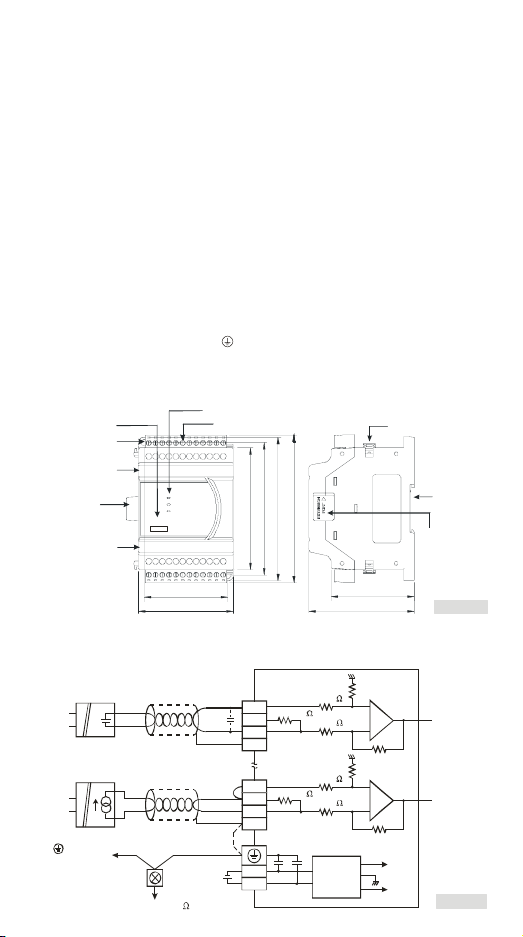
Product Profile & Dimension
[ Fig ure 1 ]
70
62
106
98
78
90
61.5
110
06XA-E2
4AI/2A O
Direct mounting
hole
Model Name
Terminal No.
I/O module
conn ection port
Ter mina l No .
Power / A<->D / Errorindicators
Removable I/O terminal
I/O module
conn ection port
I/O module clip
Mounting slot
(35mm)
(Uni t: mm)
External Wiring
y Input: Active-type
CH1
1M
250
V1+
I1+
VI1-
CH1
CH4
V4+
I4+
VI4-
CH4
*3
*2
AG
0V
24V
DC/DC
+15V
-15V
AG
FE
FE
Volta ge input
Current input
Shielded cable*1
Shielded cable*1
Te rmi nal of
power module
Grounding
(100 or less)
Convert er
[ Fig ure 2 ]
1M
1M
250
AG
1M
+
-
U
IN
+
-
U
IN

- 2 -
y Input: Passive-type
CH1
1M
250
V1+
I1+
VI1-
CH1
CH4
V4+
I4+
VI4-
CH4
*3
*2
AG
0V
24V
DC/DC
+15V
-15V
AG
FE
FE
Volta ge input
Current input
Shielded cable*1
Shielded cable*1
Te rmi nal of
power module
Grounding
(100 or less)
Converter
[ Fig ure 3 ]
1M
1M
250
AG
1M
-
+
U
IN
-
+
y Output
VO1
IO1
AG
CH5
*5
CH5
Voltage output
AC motor d rive,
recorder,
scale valve...
Shielded cable*4
VO2
IO2
AG
CH6
CH6
0V
24V
DC24V
DC/DC
+15V
-15V
AG
Class 3 grounding (100 or less)
converter
Shielded cable*4
Current output
Te rmi nal o f
power module
AC motor d rive,
recorder,
scale valve...
[ Fig ure 4 ]
*1: When performing analog input, please isolate other power wirings.
*2: When the XA module is connected to current signals, make sure you short-circuit "V+” and “I+”
terminals.
*3: If the ripples at the loaded input terminal are too significant that causes noise interference on the
wiring, connect the wiring to 0.1 ~ 0.47μF 25V capacitor.
*4: When performing analog output, please isolate other power wirings.
*5: If the ripples at the loaded output terminal are too significant that causes noise interference on the
wiring, connect the wiring to 0.1 ~ 0.47μF 25V capacitor.
*6: Please connect the
terminal on both the power module and XA module to the system earth point
and ground the system contact or connect it to the cover of power distribution cabinet.
I/O Terminal Layout
FEFEFE0V
24V
DVP06XA-E2 (4AI/2AO)
IO1VO1
VI2-I2+V2+VI1-I1+V1+
VI4-I4 +V4+VI3-I3+V3+
A
GIO2VO2AG
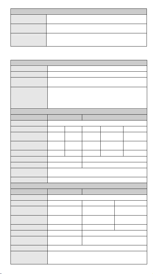
Electrical Specifications
DVP06XA-E2
Power supply voltage 24VDC (20.4VDC ~ 28.8VDC) (-15% ~ +20%)
Max. rated power
consumption
2.5W, supplied by external power source
Connector European standard removable terminal block (Pin pitch: 5mm)
- 3 -
DVP06XA-E2
Operation/storage
Operation: 0°C~55°C (temp.), 50~95% (humidity), Pollution degree2
Storage: -25°C~70°C (temp.), 5~95% (humidity)
Vibration/shock
immunity
International standards: IEC61131-2, IEC 68-2-6 (TEST Fc)/
IEC61131-2 & IEC 68-2-27 (TEST Ea)
Series connection to
DVP-PLC MPU
The modules are numbered from 0 to 7 automatically by their
distance from MPU. Max. 8 modules are allowed to connect to MPU
and will not occupy any digital I/O points.
Functions Specifications
Common specifications
Digital data format 2’s complement of 16 bits
Response time 400μs / each channel
Overall accuracy
±0.5% when in full scale within the range of (25°C, 77°F);
±1% when in full scale within the range of (0 ~ 55°C, 32 ~ 131°F)
Isolation
Optical coupler isolation between digital circuits and analog circuits.
No isolation among analog channels.
500VDC between digital circuits and Ground. 500VDC between
analog circuits and Ground. 500VDC between analog circuits and
digital circuits. 500VDC between 24VDC and Ground
Analog / Digital
Voltage input Current input
Analog input channel 4 channels / each module
Range of analog input ±10V ±5V ±20mA 0 ~ 20mA 4 ~ 20mA
Range of digital
conversion
±32,000 ± 32,000 ±32,000 0 ~ 32,000 0 ~ 32,000
Max./Min. output range
of digital data
±32,384 ±32,384 ±32,384 -384 ~+32,384 -384 ~+32,384
Hardware Resolution 14 bits 14 bits 14 bits 13 bits 13 bits
Input impedance ≧1MΩ 250Ω
Range of absolute input ±15V ±32mA
Average Function
Supported. Available for setting up sampling range in CR#8 ~
CR#11. Range: K1 ~ K100.
Self-diagnosis Upper and lower bound detection in all channels
Digital / Analog
Voltage output Current output
Analog output channel 2 channels / each module
Range of analog output -10V ~ 10V 0 ~ 20mA 4m A ~ 20mA
Range of digital
conversion
-32,000 ~ +32,000 0 ~ +32,000 0 ~ +32,000
Max./Min. input range of
digital data
-32,768 ~ +32,767 0 ~ +32,767 -6,400 ~ +32,767
Hardware Resolution 14 bits 14 bits 14 bits
Max. output current 5mA -
Tolerance load
impedance
1KΩ ~ 2MΩ 0 ~ 500Ω
Output impedance 0.5Ω or lower
Protection
Voltage output is protected by short circuit. Short circuit lasting for
too long may cause damage on internal circuits. Current output can
be open circuit.
- 4 -
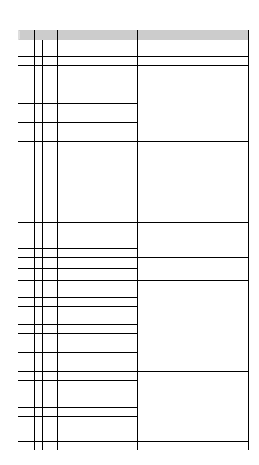
Control Register
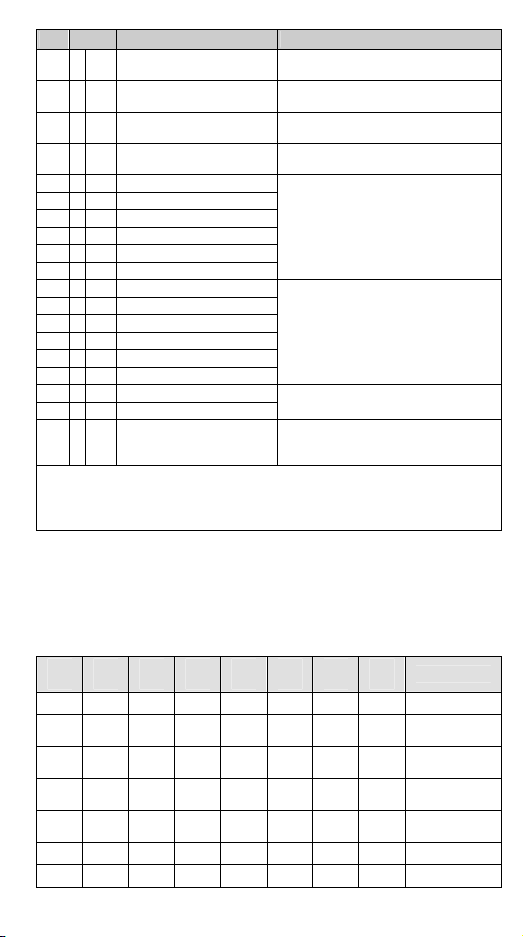
CR# Attrib. Register name Explanation
#0 O R Model name
Set up by the system:
DVP06XA-E2 model code = H’00C4
#1 O R Firmware version Display the current firmware version in hex.
#2 O R/W CH1 Input mode setting
#3 O R/W CH2 Input mode setting
#4 O R/W CH3 Input mode setting
#5 O R/W CH4 Input mode setting
Input mode: Default = H’0000. Take CH1 for
example:
Mode 0 (H’0000):Voltage input (±10V)
Mode 1 (H’0001):Voltage input (±5V)
Mode 2 (H’0002):Voltage input (0 ~+10V)
Mode 3 (H’0003):Voltage input (0 ~+5V)
Mode 4 (H’0004):Current input (±20mA)
Mode 5 (H’0005):Current input (0 ~+20mA)
Mode 6 (H’0006):Current input (4 ~+20mA)
Mode -1 (H’FFFF):Channel 1 unavailable
#6 O R/W CH5 output mode setting
#7 O R/W CH6 output mode setting
Output mode: Default = H’0000. Take CH5
for example:
Mode 0 (H’0000):Voltage output (±10V)
Mode 1 (H’0001):Current output (0~+20mA)
Mode 2 (H’0002):Current output (4~+20mA)
Mode -1 (H’FFFF):Channel 5 unavailable
#8 O R/W CH1 sampling range
#9 O R/W CH2 sampling range
#10 O R/W CH3 sampling range
#11 O R/W CH4 sampling range
Set sampling range in CH1 ~ CH4:
Range = K1 ~ K100
Default = K10
#12 X R CH1 average input value
#13 X R CH2 average input value
#14 X R CH3 average input value
#15 X R CH4 average input value
Average value of input signals at CH1 ~
CH4
#16 X
R/W
CH5 output signal value
#17 X
R/W
CH6 output signal value
Voltage output range: K-32,000~K32,000.
Current output range: K0~K32,000.
Default: K0.
#20 X R CH1 present input value
#21 X R CH2 present input value
#22 X R CH3 present input value
#23 X R CH4 present input value
Present value of input signals at CH1 ~ CH4
#28 O R/W Adjusted Offset value of CH1
#29 O R/W Adjusted Offset value of CH2
#30 O R/W Adjusted Offset value of CH3
#31 O R/W Adjusted Offset value of CH4
#32 O R/W Adjusted Offset value of CH5
#33 O R/W Adjusted Offset value of CH6
Set the adjusted Offset value of CH1 ~ CH6
Default = K0.
Definition of Offset in DVP06XA -E2:
The corresponding voltage (current) input
value when the digital output value = 0
#34 O R/W Adjusted Gain value of CH1
#35 O R/W Adjusted Gain value of CH2
#36 O R/W Adjusted Gain value of CH3
#37 O R/W Adjusted Gain value of CH4
#38 O R/W Adjusted Gain value of CH5
#39 O R/W Adjusted Gain value of CH6
Set the adjusted Gain value in CH1 ~ CH6
Default = K16,000. Definition of Gain in
DVP06XA-E2: The corresponding voltage
(current) input value when the digital output
value = 16,000.
#40 O R/W Set value changing prohibited
Prohibit set value changing in CH1 ~ CH4
Default= H’0000.
#41 X R/W Save all the set values Save all the set values, Default =H’0000
- 5 -
CR# Attrib. Register name Explanation
#42 X R/W Return to default setting
Set all values to default setting, Default =
H’0000
#43 X R Error status
Register for storing all error status. Refer to
table of error status for more information.
#100 O R/W Enable/Disable limit detection
Enable/Disable the upper and lower bound
detection function. Default= H’0000.
#101 X R/W Upper and lower bound status
Display the upper and lower bound value,
Default =H’0000
#102 O R/W Set value of CH1 upper bound
#103 O R/W Set value of CH2 upper bound
#104 O R/W Set value of CH3 upper bound
#105 O R/W Set value of CH4 upper bound
#106 O R/W Set value of CH5 upper bound
#107 O R/W Set value of CH6 upper bound
Set value of CH1~CH6 upper bound.
Default = K32000.
#108 O R/W Set value of CH1 lower bound
#109 O R/W Set value of CH2 lower bound
#110 O R/W Set value of CH3 lower bound
#111 O R/W Set value of CH4 lower bound
#112 O R/W Set value of CH5 lower bound
#113 O R/W Set value of CH6 lower bound
Set value of CH1~CH6 lower bound.
Default = K-32000.
#114 O R/W Output update time of CH5
#115 O R/W Output update time of CH6
Set output update time of CH5 ~ CH6
#118 O R/W
LV output mode setting of Ch5
~ Ch6
Set the output mode of CH5~CH6 when the
power is at LV (low voltage) condition.
Default=0
Symbols: O: When CR#41 is set to H’5678, the set value of CR will be saved.
X: set value will not be saved.
R: able to read data by using FROM instruction.
W: able to write data by using TO instruction.
Explanation on Special Registers D9900~D9999
When DVP-ES2 MPU is connected with modules, registers D9900~D9999 will be
reserved for storing values from modules. You can apply MOV instruction to operate
values in D9900~D9999.
When DVP-ES2 MPU is connected with DVP06XA-E2, the configuration of special
registers is as below:
Module
#0
Module
#1
Module
#2
Module
#3
Module
#4
Module
#5
Module
#6
Module
#7
Description
D1320 D1321 D1322 D1323 D1324 D1325 D1326 D1327 Model Code
D9900 D9910 D9920 D9930 D9940 D9950 D9960 D9970
CH1 average
input value
D9901 D9911 D9921 D9931 D9941 D9951 D9961 D9971
CH2 average
input value
D9902 D9912 D9922 D9932 D9942 D9952 D9962 D9972
CH3 average
input value
D9903 D9913 D9923 D9933 D9943 D9953 D9963 D9973
CH4 average
input value
D9904 D9914 D9924 D9934 D9944 D9954 D9964 D9974 CH5 output value
D9905 D9915 D9925 D9935 D9945 D9955 D9965 D9975 CH6 output value
Note 1: D9900 ~ D9999 are average input values of CH1 ~ CH4 and the sampling range is K1 ~ K100.
 Loading...