


2010-06-29
5011696001-A4L1
DVP-1050130-02
………………………………………………………………… ENGLISH …………………………………………………………………
Thank you for choosing Delta’s DVP series PLC. The analog input module of DVP04AD-SL series can read/write the data of analog input module by using instructions FROM/TO via DVP SV/EH2-L MPU program. The analog input module receives 16bit digital data of 4 groups from PLC MPU and converts it into 4 points analog input signal either in voltage or in current. Users can select input from voltage or current via wiring. Voltage input range is -10V~10VDC (resolution is 312.5μV). Current input range is -20mA ~ 20mA (resolution is 625nA).
This instruction sheet provides only information on the electrical specification, general functions, installation and wiring. For detailed program design and applicable instructions, please refer to “DVP-ES2 Operation Manual: Modules”. For details of the optional peripheral, please refer to the instruction sheet enclosed in the package. This is an OPEN TYPE I/O module and therefore should be installed in an enclosure free of airborne dust, humidity, electric shock and vibration. The enclosure should prevent non-maintenance staff from operating the device (e.g. key or specific tools are required for operating the enclosure) in case danger and damage on the device may occur.
DO NOT connect the input AC power supply to any of the I/O terminals; otherwise serious damage may occur. Check all the wiring again before switching on the power. Make sure the ground terminal  is correctly grounded in order to prevent electromagnetic interference.
Tightening torque for I/O terminal block is 1.95 kg-cm (1.7 in-lbs) and please uses 60/75°C copper conductors only.
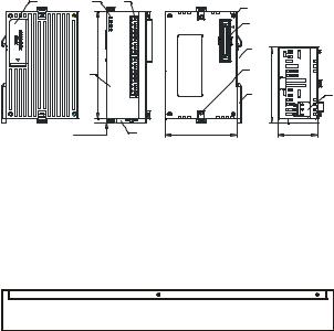
Product Profile & Dimension
1 |
2 |
4 |
|
6 |
|
|
|
|
|
|
|
|
[3.543] |
|
|
7 |
|
|
|
|
8 |
|
|
|
90 |
|
|
|
[2.496]63.4 |
|
DVP-04AD |
|
|
9 |
|
|
3 |
|
|
|
|
|
|
|
|
5 |
|
|
3 [0.118] |
5 |
60 [2.362] |
|
33.1 [1.303] |
|
|
|
|
|
10
|
|
|
|
|
|
|
|
|
|
|
|
|
|
|
|
|
|
|
|
|
|
|
Unit: mm [inch] |
|
|
|
|
|
|
|
|
[ Figure 1 ] |
|
||||||||||||||||||||||
|
|
|
|
|
|
|
|
|
|
|
|
|
|
|
|
|
|
|
|
|
|
|
|
|
|
|
|
|
|
|
|
|
|
|
|
|
|
|
|
|
|
|
|
|
|
|
|
|
|
|
|
|
|||
1. |
I/O module connection port |
6. |
|
Mounting hole of the I/O module |
|
||||||||||||||||||||||||||||||||||||||||||||||||||
2. |
Status indicator |
|
|
|
|
|
|
|
|
|
7. |
|
I/O module connection port |
|
|||||||||||||||||||||||||||||||||||||||||
|
|
(POWER, RUN and ERROR) |
|
|
|||||||||||||||||||||||||||||||||||||||||||||||||||
|
|
|
|
|
|
|
|
|
|
|
|
|
|
|
|
|
|
|
|
|
|
|
|
|
|
|
|
|
|
|
|
|
|
||||||||||||||||||||||
3. |
Model name |
|
|
|
|
|
|
|
|
|
8. |
|
Mounting slot (35mm) |
|
|||||||||||||||||||||||||||||||||||||||||
4. |
I/O terminals |
|
|
|
|
|
|
|
|
|
9. |
|
I/O module clip |
|
|
|
|
|
|
|
|
|
|
|
|
|
|
|
|||||||||||||||||||||||||||
5. |
Mounting slot clip |
|
|
|
|
|
|
|
|
|
10. |
|
DC power input |
|
|
|
|
|
|
|
|
|
|
|
|
|
|
|
|||||||||||||||||||||||||||
I/O Terminal Layout |
|
|
|
|
|
|
|
|
|
|
|
|
|
|
|
|
|
|
|
|
|
|
|
|
|
|
|
|
|
|
|
|
|||||||||||||||||||||||
|
V1+ |
|
I1+ |
|
V1- |
|
FG |
|
V2+ |
|
I2+ |
|
V2- |
|
FG |
|
|
|
V3+ |
|
I3+ |
|
V3- |
|
FG |
|
V4+ |
|
I4+ |
|
V4- |
|
FG |
|
|
|
|
|
|||||||||||||||||
|
|
|
|
|
|
|
|
|
|
|
|
|
|
|
|
|
|
|
|
||||||||||||||||||||||||||||||||||||
|
|
|
|
|
CH1 |
|
|
|
|
|
Ch2 |
|
|
|
|
|
|
|
|
|
Ch3 |
|
|
|
|
|
Ch4 |
|
|
|
|||||||||||||||||||||||||
|
|
|
|
|
|
|
|
|
|
|
|
|
|
|
|
|
|
|
|
|
|
|
|
|
|
|
|||||||||||||||||||||||||||||
|
|
|
|
|
|
|
|
|
|
|
|
|
|
|
|
|
|
|
|
|
|
|
|
||||||||||||||||||||||||||||||||
DVP04AD-SL (4AI) |
|
|
|
|
|
|
|
|
|
|
|
|
|
|
|
|
|
|
|
|
|
|
|
|
|
|
|
|
|
|
|
|
|
|
|
|
|
|
|
|
|
||||||||||||||
|
|
|
|
|
|
|
|
|
|
|
|
|
|
|
|
|
|
|
|
|
|
|
|
- 1 - |
|
|
|
|
|
|
|
|
|
|
|
|
|
|
|
|
|
|
|
|
|
|
|
|
|
|
|
||||

External Wiring
yActive-type
Voltage input |
CH1 |
+ |
|
|
|
|
|
|
|
|
|
|
|
|
|
|
|
|
V1+ |
|||||||
|
|
|
|
|
|
|
|
|
|
|
|
|
|
|
|
|||||||||
UIN |
|
|
|
|
|
|
|
|
|
|
|
|
|
|
|
|
*5 |
|
|
I1+ |
||||
- |
|
|
|
|
|
|
|
|
|
|
|
|
|
|
||||||||||
|
|
|
|
Shielded cable*1 |
|
|
|
|
|
|
|
VI1- |
||||||||||||
|
|
|
|
|
|
|
|
|
||||||||||||||||
|
|
|
|
|
|
|
|
|
|
|
|
FE |
||||||||||||
|
|
Current input |
CH4 |
|
|
|
|
|||||||||||||||||
|
|
|
|
|
|
|||||||||||||||||||
|
|
|
|
|
|
|||||||||||||||||||
|
|
|
|
|
|
|||||||||||||||||||
|
|
|
|
|
|
|
|
|
|
|
|
|
|
|
|
|
V4+ |
|||||||
|
|
+ |
|
|
|
|
|
|
|
|
|
|
|
|
*2 |
|
||||||||
UIN |
|
|
|
|
|
|
|
|
|
|
|
|
|
|
|
|
|
|
|
|
I4+ |
|||
|
|
|
|
|
|
|
|
VI4- |
||||||||||||||||
- |
|
|
|
|
|
|
|
|
|
|
|
|
|
|
|
|
FE |
|||||||
|
|
|
|
|
|
|
Shielded cable*1 |
*3 |
|
|||||||||||||||
|
|
|
|
|
|
|
|
|
|
|
|
|||||||||||||
Terminal of |
|
|
|
|
|
|||||||||||||||||||
|
|
|
|
|
|
|
|
|||||||||||||||||
power module |
|
|
|
|
|
|
|
|
|
|
|
|
|
|
||||||||||
*4 |
|
|
|
|
|
|
|
0V |
||||||||||||||||
|
|
|
|
|
|
|||||||||||||||||||
|
|
|
|
|
|
|
|
|
|
|
|
System |
|
|
|
|
24V |
|||||||
|
|
|
|
|
|
|
|
|
|
|
|
|
|
|
||||||||||
|
|
|
|
|
|
|
|
|
|
|
|
grounding |
|
|
|
|
|
|
|
|
||||
|
|
|
|
|
|
|
|
|
|
|
|
|
|
|
|
|
|
|
||||||
Grounding (100 or less)
y Passive-type
|
AG |
|
1M |
|
|
250 |
CH1 |
|
1M |
|
|
|
AG |
|
1M |
|
|
250 |
CH4 |
|
1M |
|
|
DC/DC |
+15V |
|
AG |
||
Converter |
||
|
-15V |
[ Figure 2 ]
Voltage input |
|
|
|
|
|
AG |
|
|
|
|
|
|
|
+ |
|
CH1 |
V1+ |
|
1M |
|
UIN |
|
|
250 |
|
CH1 |
|
|
*5 |
I1+ |
1M |
|||
- |
|
|
|
|||
|
|
VI1- |
|
|
|
|
|
|
|
|
|
|
|
|
Shielded cable*1 |
FE |
|
|
|
|
|
|
|
|
AG |
||
|
|
|
|
|
|
|
Current input |
|
CH4 |
V4+ |
|
1M |
|
|
*2 |
250 |
|
CH4 |
||
|
|
|
||||
- |
|
I4+ |
1M |
|||
|
|
|
|
|||
+ |
|
|
VI4- |
|
|
|
Shielded cable*1 |
FE |
|
|
|
||
|
|
|
|
|
||
|
|
*3 |
|
|
|
|
Terminal of |
|
|
|
|
|
|
power module |
*4 |
|
0V |
|
DC/DC |
+15V |
|
|
|
AG |
|||
|
System |
24V |
|
Converter |
||
|
grounding |
|
-15V |
|||
Grounding (100 |
or less) |
|
|
|
[ Figure 3 ] |
|
|
|
|
|
|
|
|
Note 1: When performing analog input, please isolate other power wirings.
Note 2: When the A/D module is connected to current signals, make sure you short-circuit “V+” and “I+” terminals.
Note 3: If the noise is too significant, please connect FE to the grounding terminal.
Note 4: Please connect the  terminal on both the power module and A/D module to the system earth point and ground the system contact or connect it to the cover of power distribution cabinet.
Note 5: If the ripples at the loaded input terminal are too significant that causes noise interference on the wiring, connect the wiring to 0.1 ~ 0.47μF 25V capacitor.
Electrical Specifications
Analog / Digital module |
Voltage input |
|
|
Current input |
|
||
Power supply voltage |
24VDC (-15% ~ +20%) / 3.5W |
|
|
|
|||
DVPPS01(PS02): input 100-240VAC, output 24VDC/1A(PS02: 2A) |
|||||||
|
|||||||
Analog input channel |
4 channels / each module |
|
|
|
|||
Range of analog input |
±10V |
±5V |
|
±20mA |
0 ~ 20mA |
4 ~ 20mA |
|
Range of digital |
±32,000 |
±32,000 |
|
±32,000 |
0 ~ 32,000 |
0 ~ 32,000 |
|
conversion |
|
||||||
|
|
|
|
|
|
||
- 2 -
Analog / Digital module |
Voltage input |
|
|
|
|
Current input |
|
||||||||||
Hardware Resolution |
16 bits |
|
16 bits |
|
16 bits |
|
15 bits |
|
|
15 bits |
|||||||
Input impedance |
|
< 0.5Ω |
|
|
|
|
|
|
|
|
|
|
|||||
Overall accuracy |
|
±0.3% when in full scale (25°C, 77°F) |
|
|
|
|
|
|
|||||||||
|
±0.5% when in full scale within the range of 0 ~ 55°C (32 ~ 131°F) |
||||||||||||||||
|
|
|
|
|
|||||||||||||
Response time |
|
250μs / each channel |
|
|
|
|
|
|
|
|
|
||||||
Max. output current |
1KΩ ~ 2MΩ |
|
|
|
|
|
|
|
|||||||||
Tolerance carried |
|
|
|
|
|
|
0Ω~500Ω |
|
|||||||||
impedance |
|
|
|
|
|
|
|
||||||||||
|
|
|
|
|
|
|
|
|
|
|
|
|
|||||
Digital data format |
2’s complement of 16 bits, 15 significant bits |
|
|
|
|
||||||||||||
|
|
|
|
|
Optical coupler isolation between digital circuits and analog circuits. |
||||||||||||
|
|
|
|
|
No isolation among analog channels. |
|
|
|
|
|
|
||||||
Isolation method |
|
500VDC between digital circuits and Ground |
|
|
|
|
|||||||||||
|
500VDC between analog circuits and Ground |
|
|
|
|
||||||||||||
|
|
|
|
|
|
|
|
|
|||||||||
|
|
|
|
|
500VDC between analog circuits and digital circuits |
|
|||||||||||
|
|
|
|
|
500VDC between 24VDC and Ground |
|
|
|
|
|
|
||||||
Series connection to |
Connectable to the left side of MPU, numbered from 100 to 107 |
||||||||||||||||
according to the position of module from the closest to farthest to |
|||||||||||||||||
DVP-PLC MPU |
|
||||||||||||||||
|
MPU. |
|
|
|
|
|
|
|
|
|
|
||||||
|
|
|
|
|
|
|
|
|
|
|
|
|
|
|
|||
Operation/storage |
Operation: 0°C~55°C (temp.), 50~95% (humidity), Pollution degree2 |
||||||||||||||||
temperature |
|
Storage: -25°C~70°C (temp.), 5~95% (humidity) |
|
||||||||||||||
Vibration/shock |
|
International standards: IEC61131-2, IEC 68-2-6 (TEST Fc)/ |
|||||||||||||||
immunity |
|
|
|
IEC61131-2 & IEC 68-2-27 (TEST Ea) |
|
|
|
|
|
|
|||||||
Control Register |
|
|
|
|
|
|
|
|
|
|
|||||||
|
|
|
|
|
|
|
|
|
|
|
|
|
|
||||
CR# |
Attrib. |
|
|
Register name |
|
|
|
|
Explanation |
|
|||||||
#0 |
O |
R |
|
Model name |
|
Set up by the system: |
|
|
|
|
|||||||
|
|
DVP04AD-SL model code = H’4400 |
|||||||||||||||
|
|
|
|
|
|
|
|
||||||||||
#1 |
O |
R |
|
Firmware version |
|
Display the current firmware version in hex. |
|||||||||||
#2 |
X |
R/W |
|
CH1 input mode setting |
|
Input mode: Default = H’0000. |
|
||||||||||
|
|
Take CH1 for example: |
|
|
|
|
|||||||||||
|
|
|
|
|
|
|
|
|
|
|
|
||||||
|
|
|
|
|
|
|
|
Mode 0 (H’0000): Voltage input (±10V) |
|||||||||
|
|
|
|
|
|
|
|
||||||||||
#3 |
X |
R/W |
|
CH2 input mode setting |
|
Mode 1 (H’0001): Current input (±20mA) |
|||||||||||
|
|
Mode 2 (H’0002): Current input (0~+20mA) |
|||||||||||||||
|
|
|
|
|
|
|
|
||||||||||
#4 |
X |
R/W |
|
CH3 input mode setting |
|
Mode 3 (H’0003): Current input (+4~+20mA) |
|||||||||||
|
|
Mode 4 (H’0004): Voltage input (±5V) |
|||||||||||||||
|
|
|
|
|
|
|
|
Mode 5 (H’0005): Voltage input (0V~+5V) |
|||||||||
|
|
|
|
|
|
|
|
||||||||||
#5 |
X |
R/W |
|
CH4 input mode setting |
|
Mode 6 (H’0006): Voltage input (1V~+5V) |
|||||||||||
|
|
Mode -1 (H’FFFF): Channel 1 unavailable |
|||||||||||||||
|
|
|
|
|
|
|
|
||||||||||
|
|
|
|
|
|
|
|
b15 ~ b12 |
b11 ~ b8 |
b7 ~ b4 |
|
b3 ~ b0 |
|||||
|
|
|
|
|
|
|
|
CH4 |
|
CH3 |
CH2 |
|
CH1 |
||||
#6 |
X |
R/W |
|
History mode |
|
Only average values are recorded. |
|
||||||||||
|
|
Default = H’0000. Take CH1 for example: |
|||||||||||||||
|
|
|
|
|
|
|
|
K0: Disable (Default). K1: Single. K2: Auto. |
|||||||||
|
|
|
|
|
|
|
|
K3: Rising Edge Triggered |
|
||||||||
|
|
|
|
|
|
|
|
K4: Falling Edge Triggered |
|
||||||||
#7 |
X |
R/W |
|
History command |
|
Refer to table of history command for detail. |
|||||||||||
|
|
Default = H’0000 |
|
|
|
|
|||||||||||
|
|
|
|
|
|
|
|
|
|
|
|
||||||
- 3 -
CR# |
Attrib. |
Register name |
Explanation |
||
#8 |
X |
R/W |
CH1 sampling range |
Set sampling range in CH1 ~ CH4: |
|
#9 |
X |
R/W |
CH2 sampling range |
||
Range = K1 ~ K20 |
|||||
#10 |
X |
R/W |
CH3 sampling range |
||
Default = K10 |
|||||
#11 |
X |
R/W |
CH4 sampling range |
||
|
|||||
#12 |
X |
R |
CH1 average input value |
|
|
#13 |
X |
R |
CH2 average input value |
Average value of input signals at CH1 ~ CH4 |
|
#14 |
X |
R |
CH3 average input value |
||
|
|||||
#15 |
X |
R |
CH4 average input value |
|
|
#16 |
X |
R |
CH1 present input value |
|
|
#17 |
X |
R |
CH2 present input value |
Present value of input signals at CH1 ~ CH4 |
|
#18 |
X |
R |
CH3 present input value |
||
|
|||||
#19 |
X |
R |
CH4 present input value |
|
|
#20 |
X |
R/W |
Set value of CH1 upper bound |
|
|
#21 |
X |
R/W |
Set value of CH2 upper bound |
Set value of CH1~CH4 upper bound. |
|
#22 |
X |
R/W |
Set value of CH3 upper bound |
Default = K32767. |
|
#23 |
X |
R/W |
Set value of CH4 upper bound |
|
|
#24 |
X |
R/W |
Set value of CH1 lower bound |
|
|
#25 |
X |
R/W |
Set value of CH2 lower bound |
Set value of CH1~CH4 lower bound. |
|
#26 |
X |
R/W |
Set value of CH3 lower bound |
Default = K-32768. |
|
#27 |
X |
R/W |
Set value of CH4 lower bound |
|
|
#28 |
X |
R/W |
Adjusted Offset value of CH1 |
Set the adjusted Offset value of CH1 ~ CH4. |
|
|
|
|
|
Default = K0 |
|
#29 |
X |
R/W |
Adjusted Offset value of CH2 |
||
Definition of Offset in DVP04AD-SL: |
|||||
#30 |
X |
R/W |
Adjusted Offset value of CH3 |
||
The corresponding voltage (current) input |
|||||
#31 |
X |
R/W |
Adjusted Offset value of CH4 |
value when the digital input value = 0. |
|
#34 |
X |
R/W |
Adjusted Gain value of CH1 |
Set the adjusted Gain value in CH1 ~ CH4. |
|
#35 |
X |
R/W |
Adjusted Gain value of CH2 |
Default = K16,000 |
|
Definition of Gain in DVP04AD-SL: |
|||||
|
|
|
|
||
#36 |
X |
R/W |
Adjusted Gain value of CH3 |
||
The corresponding voltage (current) input |
|||||
#37 |
X |
R/W |
Adjusted Gain value of CH4 |
value when the digital input value = 16,000. |
|
#38 |
X |
R/W |
CH1 Edge value |
|
|
#39 |
X |
R/W |
CH2 Edge value |
Default = K0 |
|
#40 |
X |
R/W |
CH3 Edge value |
||
|
|||||
#41 |
X |
R/W |
CH4 Edge value |
|
|
|
|
|
|
b0 ~ b3: reset CH1 ~ CH4 |
|
|
|
|
Function: Return to default |
b4 ~ b15: reserved |
|
#42 |
X |
R/W |
Default = H’0000. Give CH1 setting for |
||
setting |
|||||
|
|
|
|
example: When b0 is set to 1, all settings are |
|
|
|
|
|
reset to default setting. |
|
|
|
|
|
Register for storing all error status. Refer to |
|
#43 |
X |
R |
Error status |
table of error status for more information. |
|
|
|
|
|
Default = H’0000. |
|
#44 |
X |
R |
History status |
Refer to table of history status for detail. |
|
Default = K1 |
|||||
|
|
|
|
||
- 4 -
CR# |
Attrib. |
Register name |
|
Explanation |
|
|||
#46 |
X |
R |
CH1 History timer |
|
Set history timer in CH1 ~ CH4: |
|
||
#47 |
X |
R |
CH2 History timer |
|
|
|||
|
Range = K1 ~ K32767 |
|
||||||
#48 |
X |
R |
CH3 History timer |
|
|
|||
|
Default = K1 |
|
||||||
#49 |
X |
R |
CH4 History timer |
|
|
|||
|
|
|
||||||
#100 ~ #199 |
CH1 ~ CH4 history |
|
|
|
||||
Symbols: O means latched. X means not latched. |
|
|||||||
|
|
|
R means can read data by using FROM instruction. |
|
||||
|
|
|
W means can write data by using TO instruction. |
|
||||
|
|
|
LSB (Least Significant Bit):1. Voltage input: 1LSB=10V/32,000=312.5μV |
|
||||
|
|
|
|
|
2. Current input: 1LSB=20mA/32,000=625nA |
|
||
CR#7 History command. See the table below. |
|
|||||||
|
|
|
|
|
|
|
|
|
|
|
|
CMD |
|
|
|
History Command |
|
|
|
H’1000 ~ H’1003 |
|
|
CH1 ~ CH4 start |
|
||
|
|
H’2000 ~ H’2003 |
|
|
CH1 ~ CH4 stop |
|
||
|
|
H’4000 ~ H’4003 |
|
Reset history buffers of CH1 ~ CH4 |
|
|||
|
|
H’6000 ~ H’6003 |
|
Read histories of CH1 ~ CH4 |
|
|||
Note: Please use pulse instruction for executing history commands When the instruction is completed, the CR will be reset to 0.
CR#43: Error status value. See the table below. |
|
|
|
|
||||
|
|
|
|
|
|
|
|
|
|
Bit |
Error Status |
Content Value |
Bit |
|
Error Status |
|
Content Value |
|
b0 |
K1 (H’0001) |
Power supply error |
b1 |
K2 (H’0002) |
Hardware error |
||
|
|
|
|
|
|
|
|
|
|
b2 |
K4 (H’0004) |
Mode setting error |
|
|
b3 ~ b7 Reserved |
||
|
b8 |
K256 (H’0100) |
CH1 Conversion error |
b9 |
K512 (H’0200) |
CH2 Conversion error |
||
|
|
|
|
|
|
|
||
|
b10 |
K1024 (H’0400) |
CH3 Conversion error |
b11 |
K2048 (H’0800) |
CH4 Conversion error |
||
|
|
|
|
|
|
|
|
|
|
b12 |
K4096 (H’1000) |
CH1 Upper / lower |
b13 |
K8192 (H’2000) |
CH2 Upper / lower |
||
|
bound error |
bound error |
||||||
|
b14 |
K16384 |
CH3 Upper / lower |
b15 |
K32768 |
CH4 Upper / lower |
||
|
(H’4000) |
bound error |
(H’8000) |
bound error |
||||
Note: Each error status is determined by the corresponding bit and there may be more than 2 errors occurring at the same time. 0 = normal; 1 = error.
CR#44: History status. See the table below. |
|
|
|
|
|
|
|
|
|
||||||
b15 |
b14 |
b13 |
b12 |
b11 |
b10 |
b9 |
b8 |
b7 |
b6 |
b5 |
b4 |
b3 |
b2 |
b1 |
b0 |
Value |
|
|
|
|
|
|
|
|
|
|
|
|
|
|
|
Ch4 Ch3 Ch2 Ch1 Ch4 Ch3 Ch2 Ch1 Ch4 Ch3 Ch2 Ch1 Ch4 Ch3 Ch2 Ch1 |
|||||||||||||||
0 |
Not Ready |
|
|
Not Full |
|
|
Empty |
|
|
Stop |
|
||||
1 |
Ready |
|
|
Full |
|
|
Not Empty |
|
|
Run |
|
||||
Note: History Command for reading will be executed only when a set of full 100 records are ready. If there are less than 100 records, Not Ready will be indicated.
bit 8 ~ bit11 = 1: History buffer full. bit12 ~ bit15 = 1: History buffer ready.
Adjust A/D Conversion Curve
Users can adjust the conversion curves according to the actual needs by changing the Offset value (CR#28 ~ CR#31) and Gain value (CR#34 ~ CR#37).
- 5 -
Gain: The corresponding voltage/current input value when the digital output value = 16,000.
Offset: The corresponding voltage/current input value when the digital output value = 0. y Equation for voltage input Mode0: 0.3125mV = 20V/64,000 = 10V/32,000
|
X (V ) |
|
(Gain −Offset ) |
Y =16000 × |
|
×32000 −Offset |
|
|
10(V ) |
|
Y=Digital output, X=Voltage input |
yEquation for voltage input Mode4 / Mode5 / Mode6: 0.15625mV = 10V/64,000 = 5V/32,000
|
X (V ) |
|
(Gain −Offset) |
Y =16000 × |
|
×32000 −Offset |
|
|
5(V ) |
|
Y=Digital output, X=Voltage input |
y Equation for current input Mode1 / Mode2: 0.625μA = 40mA/64,000 = 20mA/32,000
|
X (mA) |
|
(Gain −Offset) |
Y =16000 × |
|
×32000 −Offset |
|
|
20(mA) |
|
Y=Digital output, X=Current input |
yEquation for current input Mode3: 0.5μA = 16mA/32,000
Adopt the Equation of current input Mode3, substitute Gain for 19200 (12mA) and Offset for 6400 (4mA)
|
X (mA) |
×32000 |
|
(19200 −6400) |
|
|
|
Y =16000 × |
20(mA) |
−6400 |
|
|
|||
|
|
|
|
|
Y=Digital output, X=Current input |
||
y Mode 0: |
|
|
|
|
y Mode 1: |
|
|
|
+32384 |
|
|
|
|
+32384 |
|
|
+32000 |
|
|
|
|
+32000 |
|
Digital |
|
|
|
|
Digital |
|
|
output |
+16000 |
|
|
|
output |
+16000 |
|
|
|
|
|
|
|
||
-10V |
0 |
|
5V |
|
-20mA |
0 |
10mA |
|
|
|
|
||||
|
|
|
|
10V |
|
|
20mA |
|
|
Offset |
Gain |
|
|
Offset |
Gain |
|
|
-16000 |
|
|
|
-16000 |
|
|
|
Voltage input |
|
Current input |
|||
|
|
-32000 |
|
|
|
-32000 |
|
|
|
-32384 |
|
|
|
-32384 |
|
Mode 0 of CR#2 ~ CR#5 |
-10V ~ +10V Gain = 5V (16,000) Offset = 0V (0) |
|
Mode 1 of CR#2 ~ CR#5 |
20mA ~ +20mA Gain = 10mA (16,000) Offset = 0V (0) |
|
Range of digital conversion |
-32,000 ~ +32,000 |
|
Max./Min. range of digital |
-32,384 ~ +32,384 |
|
conversion |
||
|
y Mode 2: |
|
|
|
y Mode 3: |
|
|
|
|
+32384 |
|
|
|
+32384 |
|
|
|
+32000 |
|
|
|
+32000 |
|
|
Digital |
|
|
|
Digital |
|
|
|
output |
+16000 |
|
|
output |
+16000 |
|
|
|
|
|
|
|
|
||
|
|
Gain |
|
|
|
Gain |
|
|
0 |
|
|
|
0 |
|
|
|
-384 |
10mA |
20mA |
|
-384 |
4mA 12mA |
20mA |
|
|
Offset |
|
|
|
Offset |
|
|
|
Current input |
|
|
Current input |
||
|
|
|
|
- 6 - |
|
|
|
 Loading...