


2010-04-22
5011686201-E2A1
DVP-1130130-02
………………………………………………………………… ENGLISH …………………………………………………………………
Thank you for choosing Delta’s DVP series PLC. DVP04AD-E2 analog input module receives external 4 points of analog input signals (voltage or current) and converts them into 16-bit digital signals. You can select voltage input or current input by the wiring. In addition, you can access the data in the module by applying FROM/TO instructions or read the average value of channels directly by using MOV instruction (Please refer to allocation of special registers D9900 ~ D9999).
This instruction sheet provides only information on the electrical specification, general functions, installation and wiring. For detailed program design and applicable instructions, please refer to “DVP-ES2 Operation Manual: Modules”. For details of the optional peripheral, please refer to the instruction sheet enclosed in the package.
This is an OPEN TYPE I/O module and therefore should be installed in an enclosure free of airborne dust, humidity, electric shock and vibration. The enclosure should prevent non-maintenance staff from operating the device (e.g. key or specific tools are required for operating the enclosure) in case danger and damage on the device may occur.
DO NOT connect the input AC power supply to any of the I/O terminals; otherwise serious damage may occur. Check all the wiring again before switching on the power. Make sure the ground terminal  is correctly grounded in order to prevent electromagnetic interference.
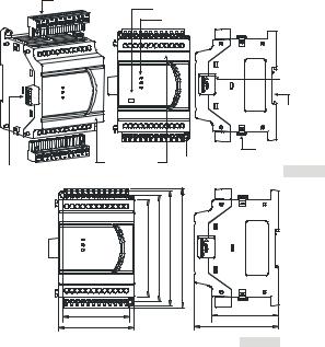
Product Profile & Dimension
Removable I/O terminal |
|
Model Name |
|
|
Power / A->D / Error indicators |
|
I/O module |
|
connection port |
04AD-E2 |
|
4AI |
|
|
Mounting slot |
|
(35mm) |
|
I/O module clip |
I/O terminal No. |
Direct mounting hole |
I/O module connection port |
[ Figure 1 ] |
90 |
98 |
106 |
110 |
|
62 |
|
|
|
61.5 |
|
|
|
|
|
70 |
|
|
|
78 |
|
Unit:mm |
[ Figure 2 ] |
||
- 1 -

External Wiring
yActive-type
Voltage input |
CH1 |
+ |
|
|
|
|
|
|
|
|
|
|
|
|
|
|
|
|
V1+ |
|||||||
|
|
|
|
|
|
|
|
|
|
|
|
|
|
|
|
|||||||||
UIN |
|
|
|
|
|
|
|
|
|
|
|
|
|
|
|
|
*5 |
|
|
I1+ |
||||
- |
|
|
|
|
|
|
|
|
|
|
|
|
|
|
||||||||||
|
|
|
|
Shielded cable*1 |
|
|
|
|
|
|
|
VI1- |
||||||||||||
|
|
|
|
|
|
|
|
|
||||||||||||||||
|
|
|
|
|
|
|
|
|
|
|
|
FE |
||||||||||||
|
|
Current input |
CH4 |
|
|
|
|
|||||||||||||||||
|
|
|
|
|
|
|||||||||||||||||||
|
|
|
|
|
|
|||||||||||||||||||
|
|
|
|
|
|
|||||||||||||||||||
|
|
|
|
|
|
|
|
|
|
|
|
|
|
|
|
|
V4+ |
|||||||
|
|
+ |
|
|
|
|
|
|
|
|
|
|
|
|
*2 |
|
||||||||
UIN |
|
|
|
|
|
|
|
|
|
|
|
|
|
|
|
|
|
|
|
|
I4+ |
|||
|
|
|
|
|
|
|
|
VI4- |
||||||||||||||||
- |
|
|
|
|
|
|
|
|
|
|
|
|
|
|
|
|
FE |
|||||||
|
|
|
|
|
|
|
Shielded cable*1 |
*3 |
|
|||||||||||||||
|
|
|
|
|
|
|
|
|
|
|
|
|||||||||||||
Terminal of |
|
|
|
|
|
|||||||||||||||||||
|
|
|
|
|
|
|
|
|||||||||||||||||
power module |
|
|
|
|
|
|
|
|
|
|
|
|
|
|
||||||||||
*4 |
|
|
|
|
|
|
|
0V |
||||||||||||||||
|
|
|
|
|
|
|||||||||||||||||||
|
|
|
|
|
|
|
|
|
|
|
|
System |
|
|
|
|
24V |
|||||||
|
|
|
|
|
|
|
|
|
|
|
|
|
|
|
||||||||||
|
|
|
|
|
|
|
|
|
|
|
|
grounding |
|
|
|
|
|
|
|
|
||||
|
|
|
|
|
|
|
|
|
|
|
|
|
|
|
|
|
|
|
||||||
Grounding (100 or less)
|
AG |
|
1M |
|
|
250 |
CH1 |
|
1M |
|
|
|
AG |
|
1M |
|
|
250 |
CH4 |
|
1M |
|
|
DC/DC |
+15V |
|
AG |
||
Converter |
||
|
-15V |
[ Figure 3 ]
y Passive-type |
|
|
|
|
|
|
Voltage input |
|
|
|
|
|
AG |
|
|
|
|
|
|
|
+ |
|
CH1 |
V1+ |
|
1M |
|
UIN |
|
|
250 |
|
CH1 |
|
|
*5 |
I1+ |
1M |
|||
- |
|
|
|
|||
|
|
VI1- |
|
|
|
|
|
|
|
|
|
|
|
|
Shielded cable*1 |
FE |
|
|
|
|
|
|
|
|
AG |
||
|
|
|
|
|
|
|
Current input |
|
CH4 |
V4+ |
|
1M |
|
|
*2 |
250 |
|
CH4 |
||
|
|
|
||||
- |
|
I4+ |
1M |
|||
|
|
|
|
|||
+ |
|
|
VI4- |
|
|
|
Shielded cable*1 |
FE |
|
|
|
||
|
|
|
|
|
||
|
|
*3 |
|
|
|
|
Terminal of |
|
|
|
|
|
|
power module |
*4 |
|
0V |
|
DC/DC |
+15V |
|
|
|
AG |
|||
|
System |
24V |
|
Converter |
||
|
grounding |
|
-15V |
|||
Grounding (100 |
or less) |
|
|
|
[ Figure 4 ] |
|
|
|
|
|
|
|
|
Note 1: When performing analog input, please isolate other power wirings.
Note 2: When the A/D module is connected to current signals, make sure you short-circuit “V+” and “I+” terminals.
Note 3: If the noise is too significant, please connect FE to the grounding terminal.
Note 4: Please connect the  terminal on both the power module and A/D module to the system earth point and ground the system contact or connect it to the cover of power distribution cabinet.
Note 5: If the ripples at the loaded input terminal are too significant that causes noise interference on the wiring, connect the wiring to 0.1 ~ 0.47μF 25V capacitor.
I/O Terminal Layout
V1+ I1+ VI1FE V2+ I2+ VI2FE V3+ I3+ VI3FE
DVP04AD-E2 (4AI)
24V 0V 

 FE V4+ I4+ VI4FE
Electrical Specifications
|
Analog / Digital module (04A/D) |
Power supply voltage |
24VDC (20.4VDC ~ 28.8VDC) (-15% ~ +20%) |
|
- 2 - |
|
|
|
|
|
|
|
Analog / Digital module (04A/D) |
|
|
||||
Max. rated power |
1W, supplied by external power source |
|
|
||||||||||
consumption |
|
|
|
|
|||||||||
|
|
|
|
|
|
|
|
|
|||||
Connector |
|
|
European standard removable terminal block (Pin pitch: 5mm) |
||||||||||
|
|
|
|
Operation: 0°C~55°C (temp.), 50~95% (humidity), Pollution degree2 |
|||||||||
Operation/storage |
|
||||||||||||
temperature |
|
|
Storage: -25°C~70°C (temp.), 5~95% (humidity) |
|
|||||||||
Vibration/shock |
|
|
International standards: IEC61131-2, IEC 68-2-6 (TEST Fc)/ |
||||||||||
immunity |
|
|
|
|
IEC61131-2 & IEC 68-2-27 (TEST Ea) |
|
|
||||||
Series connection to |
|
The modules are numbered from 0 to 7 automatically by their |
|||||||||||
|
distance from MPU. Max. 8 modules are allowed to connect to MPU |
||||||||||||
DVP-PLC MPU |
|
|
|||||||||||
|
|
and will not occupy any digital I/O points. |
|
||||||||||
|
|
|
|
|
|
|
|
||||||
Functions Specifications |
|
|
|
|
|||||||||
|
|
|
|
|
|
|
|
|
|
|
|||
Analog / Digital module |
|
Voltage input |
|
|
Current input |
|
|||||||
Analog input channel |
|
4 channels / each module |
|
|
|||||||||
Range of analog input |
|
±10V |
±5V |
|
±20mA |
0 ~ 20mA |
4 ~ 20mA |
||||||
Range of digital |
|
|
±32,000 |
±32,000 |
|
|
±32,000 |
0 ~ 32,000 |
0 ~ 32,000 |
||||
|
|
|
|
||||||||||
conversion |
|
|
|
|
|||||||||
|
|
|
|
|
|
|
|
|
|||||
Max./Min. range of |
±32,384 |
±32,384 |
|
|
±32,384 |
-384~+32,384 |
-384~+32,384 |
||||||
digital data |
|
|
|
|
|||||||||
|
|
|
|
|
|
|
|
|
|||||
Hardware Resolution |
|
14 bits |
14 bits |
|
14 bits |
13 bits |
13 bits |
||||||
Input impedance |
|
1MΩ |
|
|
|
250Ω |
|
|
|||||
Range of absolute input |
|
±15V |
|
|
|
±32mA |
|
|
|||||
Overall accuracy |
|
±0.5% when in full scale (25°C, 77°F) |
|
|
|||||||||
|
±1% when in full scale within the range of 0 ~ 55°C (32 ~ 131°F) |
||||||||||||
|
|
|
|
|
|
|
|||||||
Response time |
|
|
400μs / each channel |
|
|
|
|
||||||
|
|
|
|
|
|
||||||||
Digital data format |
|
2’s complement of 16 bits |
|
|
|||||||||
Average function |
|
Supported. Available for setting up sampling range in CR#8 ~ |
|||||||||||
|
|||||||||||||
|
CR#11. Range: K1 ~ K100. |
|
|
||||||||||
|
|
|
|
|
|
|
|
|
|||||
Self-diagnosis |
|
|
Upper and lower bound detection in all channels |
|
|||||||||
|
|
|
|
|
|
|
Optical coupler isolation between digital circuits and analog circuits. |
||||||
|
|
|
|
|
|
|
No isolation among analog channels. |
|
|
||||
Isolation method |
|
500VDC between digital circuits and Ground |
|
||||||||||
|
500VDC between analog circuits and Ground |
|
|||||||||||
|
|
|
|
|
|
|
|
||||||
|
|
|
|
|
|
|
500VDC between analog circuits and digital circuits |
|
|||||
|
|
|
|
|
|
|
500VDC between 24VDC and Ground |
|
|
||||
Control Register |
|
|
|
|
|
|
|||||||
|
|
|
|
|
|
|
|
|
|
||||
CR# |
Attrib. |
|
Register name |
|
|
Explanation |
|
|
|||||
#0 |
O |
|
R |
|
Model name |
|
|
Set up by the system: |
|
||||
|
|
|
|
DVP04AD-E2 model code = H’0080 |
|||||||||
|
|
|
|
|
|
|
|
|
|
||||
#1 |
O |
|
R |
|
Firmware version |
|
|
Display the current firmware version in hex. |
|||||
#2 |
O |
|
R/W |
|
CH1 input mode setting |
|
Input mode: Default = H’0000. |
|
|||||
|
|
|
Take CH1 for example: |
|
|||||||||
|
|
|
|
|
|
|
|
|
|
|
|||
|
|
|
|
|
|
|
|
|
|
Mode 0 (H’0000): Voltage input (±10V) |
|||
|
|
|
|
|
|
|
|
|
|
||||
#3 |
O |
|
R/W |
|
CH2 input mode setting |
|
Mode 1 (H’0001): Voltage input (±5V) |
||||||
|
|
|
|
|
|
|
|
|
|
Mode 2 (H’0002): Voltage input (0 ~ +10V) |
|||
#4 |
O |
|
R/W |
|
CH3 input mode setting |
|
Mode 3 (H’0003): Voltage input (0 ~ +5V) |
||||||
|
|
|
Mode 4 (H’0004): Current input (±20mA) |
||||||||||
|
|
|
|
|
|
|
|
|
|
||||
|
|
|
|
|
|
|
|
|
|
Mode 5 (H’0005): Current input (0 ~ +20mA) |
|||
|
|
|
|
|
|
|
|
|
|
||||
#5 |
O |
|
R/W |
|
CH4 input mode setting |
|
Mode 6 (H’0006): Current input (+4~ +20mA) |
||||||
|
|
|
|
|
|
|
|
|
|
Mode -1 (H’FFFF): Channel 1 unavailable |
|||
- 3 -

CR# |
Attrib. |
Register name |
Explanation |
||
#8 |
O |
R/W |
CH1 sampling range |
Set sampling range in CH1 ~ CH4: |
|
#9 |
O |
R/W |
CH2 sampling range |
||
Range = K1 ~ K100 |
|||||
#10 |
O |
R/W |
CH3 sampling range |
||
Default = K10 |
|||||
#11 |
O |
R/W |
CH4 sampling range |
|
|
#12 |
X |
R |
CH1 average input value |
|
|
#13 |
X |
R |
CH2 average input value |
Average value of input signals at CH1 ~ CH4 |
|
#14 |
X |
R |
CH3 average input value |
||
|
|||||
#15 |
X |
R |
CH4 average input value |
|
|
#20 |
X |
R |
CH1 present input value |
|
|
#21 |
X |
R |
CH2 present input value |
Present value of input signals at CH1 ~ CH4 |
|
#22 |
X |
R |
CH3 present input value |
||
|
|||||
#23 |
X |
R |
CH4 present input value |
|
|
#28 |
O |
R/W |
Adjusted Offset value of CH1 |
Set the adjusted Offset value of CH1 ~ CH4. |
|
#29 |
O |
R/W |
Adjusted Offset value of CH2 |
Default = K0 |
|
Definition of Offset in DVP04AD-E2: |
|||||
|
|
|
|
||
#30 |
O |
R/W |
Adjusted Offset value of CH3 |
||
The corresponding voltage (current) input |
|||||
#31 |
O |
R/W |
Adjusted Offset value of CH4 |
value when the digital output value = 0. |
|
|
|
|
|
|
|
#34 |
O |
R/W |
Adjusted Gain value of CH1 |
Set the adjusted Gain value in CH1 ~ CH4. |
|
#35 |
O |
R/W |
Adjusted Gain value of CH2 |
Default = K16,000 |
|
Definition of Gain in DVP04AD-E2: |
|||||
|
|
|
|
||
#36 |
O |
R/W |
Adjusted Gain value of CH3 |
||
The corresponding voltage (current) input |
|||||
|
|
|
|
||
#37 |
O |
R/W |
Adjusted Gain value of CH4 |
value when the digital output value = 16,000. |
|
|
|
|
|
|
|
#40 |
O |
R/W |
Function: Set value changing |
Prohibit set value changing in CH1 ~ CH4. |
|
|
|
|
prohibited |
Default= H’0000. |
|
#41 |
X |
R/W |
Function: Save all the set |
Save all the set values, Default =H’0000 |
|
values |
|||||
#42 |
X |
R/W |
Function: Return to default |
Set all values to default setting, Default = |
|
|
|
|
setting |
H’0000 |
|
#43 |
X |
R |
Error status |
Register for storing all error status. Refer to |
|
table of error status for more information. |
|||||
|
|
|
|
||
#100 |
O |
R/W |
Function: Enable/Disable limit |
Enable/Disable the upper and lower bound |
|
|
|
|
detection |
detection function. Default= H’0000. |
|
#101 |
X |
R/W |
Upper and lower bound status |
Display the upper and lower bound value, |
|
|
|
|
|
Default =H’0000 |
|
#102 |
O |
R/W |
Set value of CH1 upper bound |
|
|
#103 |
O |
R/W |
Set value of CH2 upper bound |
Set value of CH1~CH4 upper bound. Default |
|
#104 |
O |
R/W |
Set value of CH3 upper bound |
= K32000. |
|
#105 |
O |
R/W |
Set value of CH4 upper bound |
|
|
#108 |
O |
R/W |
Set value of CH1 lower bound |
|
|
#109 |
O |
R/W |
Set value of CH2 lower bound |
Set value of CH1~CH4 lower bound. Default |
|
#110 |
O |
R/W |
Set value of CH3 lower bound |
= K-32000. |
|
#111 |
O |
R/W |
Set value of CH4 lower bound |
|
|
Symbols:
O: When CR#41 is set to H’5678, the set value of CR will be saved.
X: set value will not be saved.
R: able to read data by using FROM instruction.
W: able to write data by using TO instruction.
- 4 -

CR#43: Error status value. See the table below:
|
|
Description |
|
|
|
bit0 |
K1 (H’1) |
Power supply error |
bit6 |
K64 (H’40) |
CH4 Conversion error |
|
|
|
|
|
|
bit1 |
K2 (H’2) |
Hardware error |
bit9 |
K512(H’0200) |
Mode setting error |
|
|
|
|
|
|
bit2 |
K4 (H’4) |
Upper/lower bound error |
bit10 |
K1024(H’0400) |
Sampling range error |
|
|
|
|
|
|
bit3 |
K8 (H’8) |
CH1 Conversion error |
bit11 |
K2048(H’0800) |
Upper / lower bound |
|
|
|
|
|
setting error |
bit4 |
K16 (H’10) |
CH2 Conversion error |
bit12 |
K4096(H’1000) |
Set value changing |
|
|
|
|
|
prohibited |
|
|
|
|
|
Communication |
bit5 |
K32 (H’20) |
CH3 Conversion error |
bit13 |
K8192(H’2000) |
breakdown on next |
|
|
|
|
|
module |
Note: Each error status is determined by the corresponding bit (b0 ~ b13) and there may be more than 2 errors occurring at the same time. 0 = normal; 1 = error
Explanation on Special Registers D9900~D9999
When DVP-ES2 MPU is connected with modules, registers D9900~D9999 will be reserved for storing values from modules. You can apply MOV instruction to operate values in D9900~D9999.
When DVP-ES2 MPU is connected with DVP04AD-E2, the configuration of special registers is as below:
Module |
Module |
Module |
Module |
Module |
Module |
Module |
Module |
|
Description |
|
|
#0 |
#1 |
#2 |
#3 |
#4 |
#5 |
#6 |
#7 |
|
|
||
|
|
|
|||||||||
D1320 |
D1321 |
D1322 |
D1323 |
D1324 |
D1325 |
D1326 |
D1327 |
Model Code |
|||
|
|
|
|
|
|
|
|
|
|||
D9900 |
D9910 |
D9920 |
D9930 |
D9940 |
D9950 |
D9960 |
D9970 |
CH1 average |
|||
input value |
|||||||||||
|
|
|
|
|
|
|
|
||||
D9901 |
D9911 |
D9921 |
D9931 |
D9941 |
D9951 |
D9961 |
D9971 |
CH2 average |
|||
input value |
|||||||||||
|
|
|
|
|
|
|
|
||||
D9902 |
D9912 |
D9922 |
D9932 |
D9942 |
D9952 |
D9962 |
D9972 |
CH3 average |
|||
input value |
|||||||||||
|
|
|
|
|
|
|
|
||||
D9903 |
D9913 |
D9923 |
D9933 |
D9943 |
D9953 |
D9963 |
D9973 |
CH4 average |
|||
input value |
|||||||||||
|
|
|
|
|
|
|
|
||||
Note 1: D9900 ~ D9999 are average input values of CH1 ~ CH4 and the sampling range is K1 ~ K100. When the sampling range is set to K1, the values displayed in D9900~D9999 are current values. You can use: 1. ES_AIO Configuration Function of WPLSoft or 2. FROM/TO instructions (CR#8
~CR#11) to set the sampling range as K1.
Adjust A/D Conversion Curve
Users can adjust the conversion curves according to the actual needs by changing the Offset value (CR#28 ~ CR#31) and Gain value (CR#34 ~ CR#37).
Gain: The corresponding voltage/current input value when the digital output value = 16,000.
Offset: The corresponding voltage/current input value when the digital output value = 0. y Equation for voltage input Mode0 / Mode2: 0.3125mV = 20V/64,000 = 10V/32,000
|
X (V ) |
|
(Gain −Offset ) |
Y =16000 × |
|
×32000 −Offset |
|
|
10(V ) |
|
Y=Digital output, X=Voltage input |
yEquation for voltage input Mode1 / Mode3: 0.15625mV = 10V/64,000 = 5V/32,000
-5 -
 Loading...