


DADD DLO31F-9A2, DLO31F-9, DLO31F-8MD4, DLO31F-8MD1, DLO31F-8M Datasheet
...
DLO31F
Doc #98001 DATA DELAY DEVICES, INC. 1
3/17/98 3 Mt. Prospect Ave. Clifton, NJ 07013
TTL-INTERFACED, GATED
DELAY LINE OSCILLATOR
(SERIES DLO31F)
FEATURES PACKAGES
• Continuous or keyable wave train
• Synchronizes with arbitrary gating signal
• Fits standard 14-pin DIP socket
• Low profile
• Auto-insertable
• Input & outputs fully TTL interfaced & buffered
• Available in frequencies from 2MHz to 40MHz
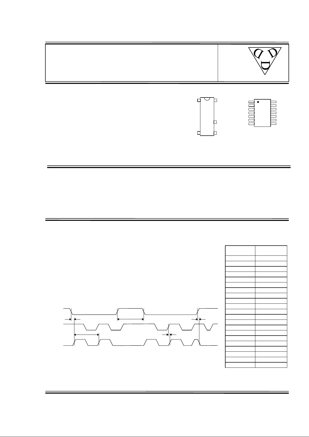
FUNCTIONAL DESCRIPTION
The DLO31F-series device is a gated delay line oscillator. The device
produces a stable square wave which is synchronized with the falling edge
of the Gate Input (GB). The frequency of oscillation is given by the device
dash number (See Table). The two outputs (C1,C2) are in phase during
oscillation, but return to opposite logic levels when the device is disabled.
SERIES SPECIFICATIONS
• Frequency accuracy: 2%
• Inherent delay (TE0): 5.5ns typical
• Output skew: 3.5ns typical
• Output rise/fall time: 2ns typical
• Supply voltage: 5VDC ± 5%
• Supply current: 40ma typical (7ma when disabled)
• Operating temperature: 0° to 70° C
• Temperature coefficient: 100 PPM/°C (See text)
GATE
(GB)
CLOCK 2
(C2)
Figure 1: Timing Diagram
CLOCK 1
(C1)
t
EO
1/f
0
t
DO
t
CS
t
GR
1998 Data Delay Devices
data
delay
devices,
inc.
3
1
2
3
4
5
6
7
14
13
12
11
10
9
8
C1
N/C
N/C
N/C
N/C
N/C
GND
VCC
N/C
N/C
N/C
C2
N/C
GB
14
10
8
1
7
C1
GND
VCC
C2
GB
DLO31F-xx DIP
DLO31F-xxA2 Gull-Wing
DLO31F-xxB2 J-Lead
DLO31F-xxM Military DIP
Military SMD
DLO31F-xxMD1
DLO31F-xxMD4
PIN DESCRIPTIONS
GB Gate Input
C1 Clock Output 1
C2 Clock Output 2
VCC +5 Volts
GND Ground
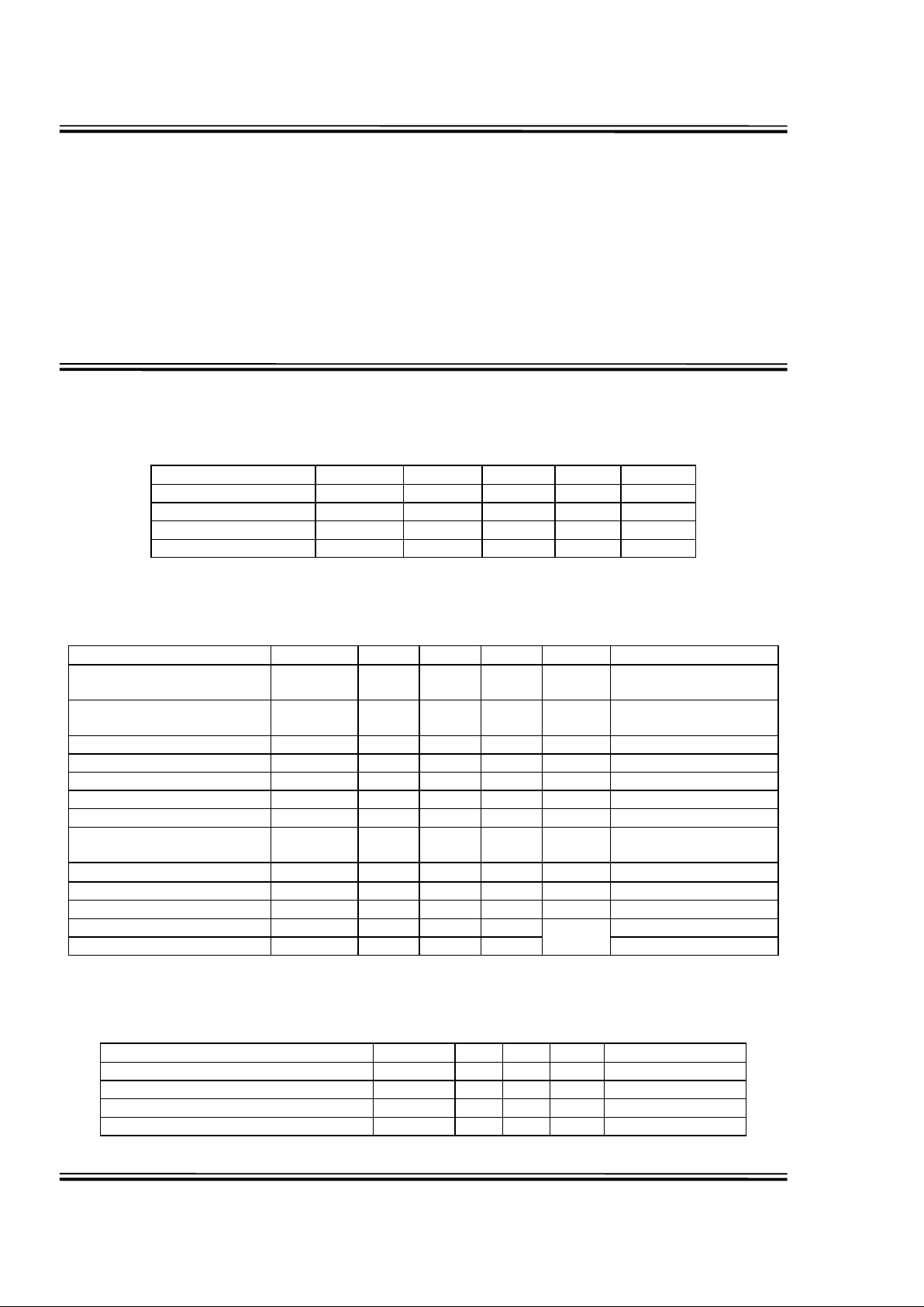
DASH NUMBER
SPECIFICATIONS
Part
Number
Frequency
(MHz)
DLO31F-2
2.0 ± 0.04
DLO31F-2.5
2.5 ± 0.05
DLO31F-3
3.0 ± 0.06
DLO31F-3.5
3.5 ± 0.07
DLO31F-4
4.0 ± 0.08
DLO31F-4.5
4.5 ± 0.09
DLO31F-5
5.0 ± 0.10
DLO31F-5.5
5.5 ± 0.11
DLO31F-6
6.0 ± 0.12
DLO31F-7
7.0 ± 0.14
DLO31F-8
8.0 ± 0.16
DLO31F-9
9.0 ± 0.18
DLO31F-10
10 ± 0.20
DLO31F-12
12 ± 0.24
DLO31F-14
14 ± 0.28
DLO31F-15
15 ± 0.30
DLO31F-20
20 ± 0.40
DLO31F-25
25 ± 0.50
DLO31F-30
30 ± 0.60
DLO31F-35
35 ± 0.70
DLO31F-40
40 ± 0.80
NOTE: Any dash number
between 2 and 40 not shown
is also available.
DLO31F
Doc #98001 DATA DELAY DEVICES, INC. 2
3/17/98 Tel: 973-773-2299 Fax: 973-773-9672 http://www.datadelay.com
APPLICATION NOTES
THERMAL STABILITY
The delay line used internally to develop the clock
signals in the DLO31F has a thermal coefficient
of 100ppm/C. For low frequency units, this is also
the thermal coefficient of the output frequency.
For higher frequency units, however, other
internal effects must be considered, and the
actual thermal coefficient may be somewhat
higher.
POWER SUPPLY BYPASSING
The DLO31F relies on a stable power supply to
produce a repeatable frequency within the stated
tolerances. A 0.1uf capacitor from VCC to GND,
located as close as possible to the VCC pin, is
recommended. A wide VCC trace and a clean
ground plane should be used.
DEVICE SPECIFICATIONS
TABLE 1: ABSOLUTE MAXIMUM RATINGS
PARAMETER SYMBOL MIN MAX UNITS NOTES
DC Supply Voltage V
CC
-0.3 7.0 V
Input Pin Voltage V
IN
-0.3 VDD+0.3 V
Storage Temperature T
STRG
-55 150 C
Lead Temperature T
LEAD
300 C 10 sec
TABLE 2: DC ELECTRICAL CHARACTERISTICS
(0C to 70C, 4.75V to 5.25V)
PARAMETER SYMBOL MIN TYP MAX UNITS NOTES
High Level Output Voltage V
OH
2.5 3.4 V VCC = MIN, IOH = MAX
VIH = MIN, VIL = MAX
Low Level Output Voltage V
OL
0.35 0.5 V VCC = MIN, IOL = MAX
VIH = MIN, VIL = MAX
High Level Output Current I
OH
-1.0 mA
Low Level Output Current I
OL
20.0 mA
High Level Input Voltage V
IH
2.0 V
Low Level Input Voltage V
IL
0.8 V
Input Clamp Voltage V
IK
-1.2 V VCC = MIN, II = I
IK
Input Current at Maximum
Input Voltage
I
IHH
0.1 mA VCC = MAX, VI = 7.0V
High Level Input Current I
IH
20
µA
VCC = MAX, VI = 2.7V
Low Level Input Current I
IL
-0.6 mA VCC = MAX, VI = 0.5V
Short-circuit Output Current I
OS
-60 -150 mA VCC = MAX
Output High Fan-out 25 Unit
Output Low Fan-out 12.5 Load
TABLE 3: AC ELECTRICAL CHARACTERISTICS
(0C to 70C, 4.75V to 5.25V)
PARAMETER SYMBOL MIN TYP MAX UNITS
Enable to Clock On (Inherent Delay) t
EO
3.5 5.5 7.0 ns
Disable to Clock Off t
DO
3.5 5.5 7.0 ns
Clock Skew t
CS
2.5 3.5 4.5 ns
Gate Recovery Time t
GR
50 % of Clock Period
 Loading...