


DADD 3D7304G-500, 3D7304G-50, 3D7304G-400, 3D7304G-40, 3D7304G-300 Datasheet
...
3D7304
MONOLITHIC QUADRUPLE
1
14
I1
VDD
data
3
FIXED DELAY LINE
(SERIES 3D7304)
FEATURES
• All-silicon, low-power CMOS technology
• TTL/CMOS compatible inputs and outputs
• Vapor phase, IR and wave solderable
• Auto-insertable (DIP pkg.)
• Low ground bounce noise
• Leading- and trailing-edge accuracy
• Delay range: 10 through 500ns
• Delay tolerance: 2% or 1.0ns
• Temperature stability: ±3% typical (0C-70C)
• Vdd stability: ±1% typical (4.75V-5.25V)
• Minimum input pulse width: 20% of total
delay
• 14-pin Gull-Wing available as drop-in replacement for hybrid delay lines
I1
N/C
I2
I3
I4
N/C
GND
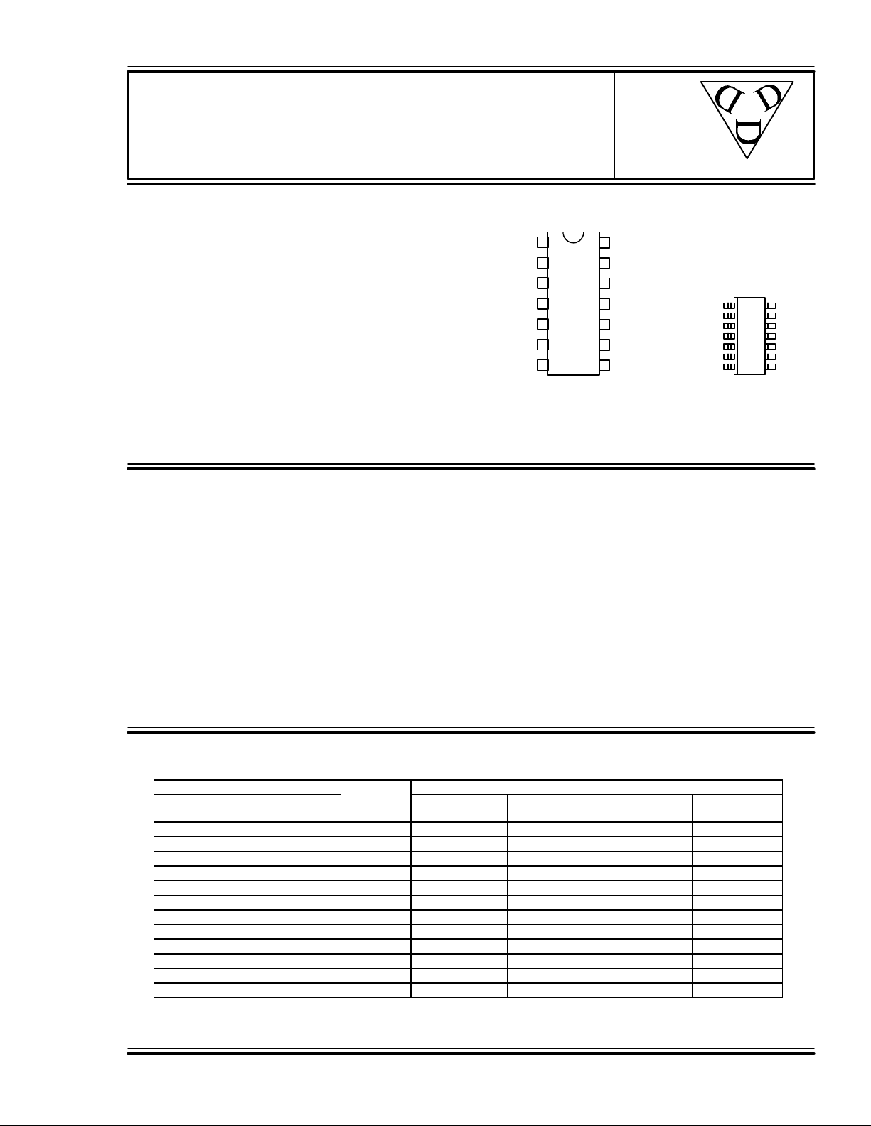
3D7304 DIP
3D7304G Gull-Wing
FUNCTIONAL DESCRIPTION
The 3D7304 Quadruple Delay Line product family consists of fixeddelay CMOS integrated circuits. Each package contains four matched,
independent delay lines. Delay values can range from 10ns through
500ns. The input is reproduced at the output without inversion, shifted
in time as per the user-specified dash number. The 3D7304 is TTLand CMOS-compatible, capable of driving ten 74LS-type loads, and
features both rising- and falling-edge accuracy.
The all-CMOS 3D7304 integrated circuit has been designed as a
reliable, economic alternative to hybrid TTL fixed delay lines. It is
offered in a standard 14-pin auto-insertable DIP and a space saving
surface mount 14-pin SOIC.
PACKAGES
14
1
13
2
12
3
11
4
10
5
9
6
8
7
(300 Mil)
delay
devices, inc.
VDD
N/C
O1
N/C
O2
O3
O4
N/C
N/C
GND
PIN DESCRIPTIONS
I1 Delay Line 1 Input
I2 Delay Line 2 Input
I3 Delay Line 3 Input
I4 Delay Line 4 Input
O1 Delay Line 1 Output
O2 Delay Line 2 Output
O3 Delay Line 3 Output
O4 Delay Line 4 Output
VCC +5 Volts
GND Ground
N/C No Connection
I2
I3
I4
3D7304D
(150 Mil)
2
13
3
12
4
11
5
10
6
7
SOIC
9
8
N/C
O1
N/C
O2
O3
O4
TABLE 1: PART NUMBER SPECIFICATIONS
PART NUMBER DELAY INPUT RESTRICTIONS
DIP-14
3D7304
-10 -10 -10
-15 -15 -15
-20 -20 -20
-25 -25 -25
-30 -30 -30
-40 -40 -40
-50 -50 -50
-100 -100 -100
-200 -200 -200
-300 -300 -300
-400 -400 -400
-500 -500 -500
NOTES: Any delay between 10 and 500 ns not shown is also available. 1996 Data Delay Devices
DIP-14
3D7304G
SOIC-14
3D7304D
PER LINE
(ns)
10 ± 1.0
15 ± 1.0
20 ± 1.0
25 ± 1.0
30 ± 1.0
40 ± 1.0
50 ± 1.0
100 ± 2.0
200 ± 4.0
300 ± 6.0
400 ± 8.0
500 ± 10.0
Max Operating
Frequency
33.3 MHz 100.0 MHz 15.0 ns 5.0 ns
22.2 MHz 100.0 MHz 22.5 ns 5.0 ns
16.7 MHz 100.0 MHz 30.0 ns 5.0 ns
13.3 MHz 83.3 MHz 37.5 ns 6.0 ns
11.1 MHz 71.4 MHz 45.0 ns 7.0 ns
8.33 MHz 62.5 MHz 60.0 ns 8.0 ns
6.67 MHz 50.0 MHz 75.0 ns 10.0 ns
3.33 MHz 25.0 MHz 150.0 ns 20.0 ns
1.67 MHz 12.5 MHz 300.0 ns 40.0 ns
1.11 MHz 8.33 MHz 450.0 ns 60.0 ns
0.83 MHz 6.25 MHz 600.0 ns 80.0 ns
0.67 MHz 5.00 MHz 750.0 ns 100.0 ns
Absolute Max
Oper. Freq.
Min Operating
Pulse Width
Absolute Min
Oper. P.W.
Doc #96002 DATA DELAY DEVICES, INC. 1
12/2/96 3 Mt. Prospect Ave. Clifton, NJ 07013
3D7304
APPLICATION NOTES
OPERATIONAL DESCRIPTION
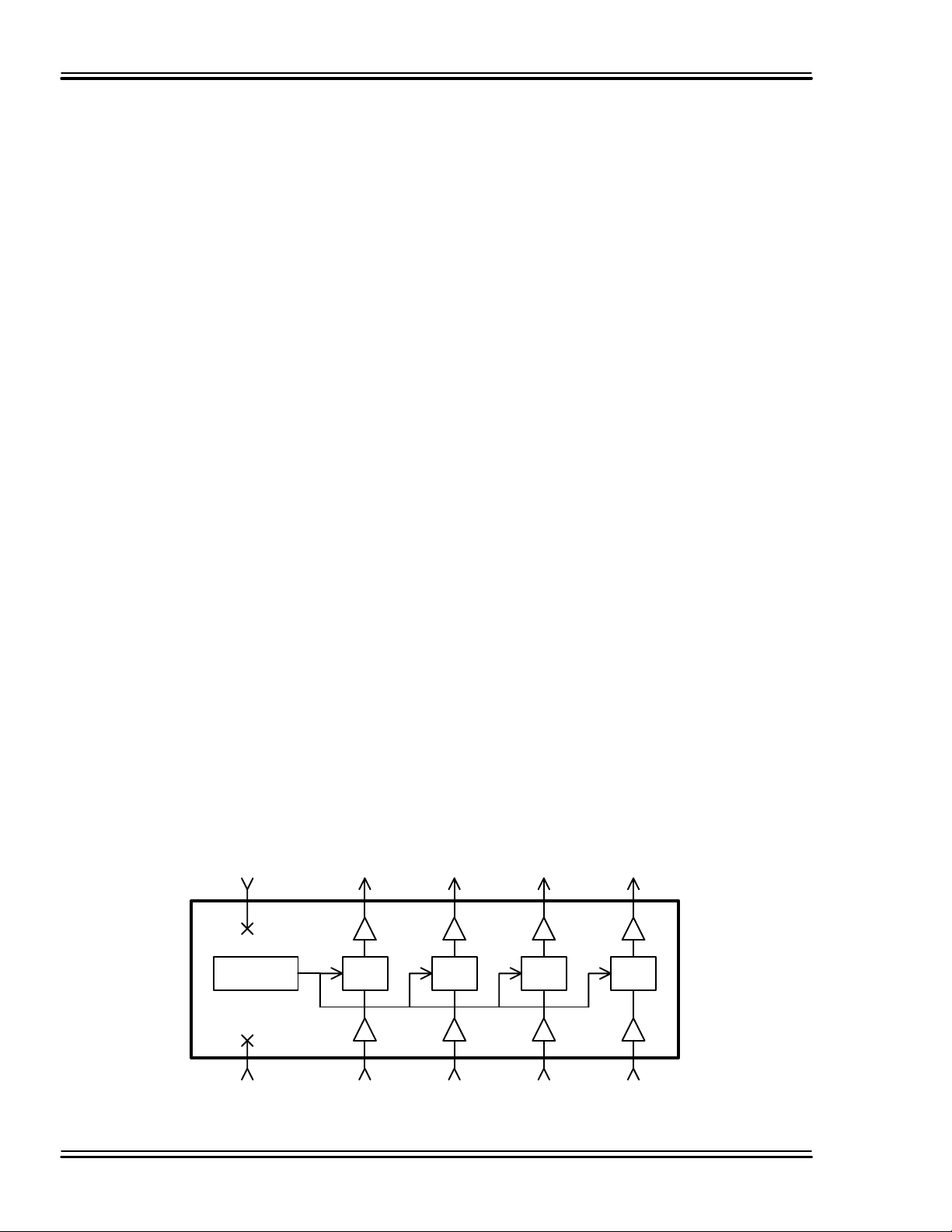
The 3D7304 quadruple delay line architecture is
shown in Figure 1. The individual delay lines are
composed of a number of delay cells connected
in series. Each delay line produces at its output
a replica of the signal present at its input, shifted
in time. The delay lines are matched and share
the same compensation signals, which
minimizes line-to-line delay deviations over
temperature and supply voltage variations.
INPUT SIGNAL CHARACTERISTICS
The Frequency and/or Pulse Width (high or low)
of operation may adversely impact the specified
delay accuracy of the particular device. The
reasons for the dependency of the output delay
accuracy on the input signal characteristics are
varied and complex. Therefore a Maximum and
an Absolute Maximum operating input
frequency and a Minimum and an Absolute
Minimum operating pulse width have been
specified.
OPERATING FREQUENCY
The Absolute Maximum Operating Frequency
specification, tabulated in Table 1, determines
the highest frequency of the delay line input
signal that can be reproduced, shifted in time at
the device output, with acceptable duty cycle
distortion.
The Maximum Operating Frequency
specification determines the highest frequency of
the delay line input signal for which the output
delay accuracy is guaranteed.
To guarantee the Table 1 delay accuracy for
input frequencies higher than the Maximum
Operating Frequency, the 3D7304 must be
tested at the user operating frequency.
Therefore, to facilitate production and device
identification, the part number will include a
custom reference designator identifying the
intended frequency of operation. The
programmed delay accuracy of the device is
guaranteed, therefore, only at the user specified
input frequency. Small input frequency variation
about the selected frequency will only marginally
impact the programmed delay accuracy, if at all.
Nevertheless, it is strongly recommended
that the engineering staff at DATA DELAY
DEVICES be consulted.
OPERATING PULSE WIDTH
The Absolute Minimum Operating Pulse
Width (high or low) specification, tabulated in
Table 1, determines the smallest Pulse Width of
the delay line input signal that can be
reproduced, shifted in time at the device output,
with acceptable pulse width distortion.
The Minimum Operating Pulse Width (high or
low) specification determines the smallest Pulse
Width of the delay line input signal for which the
output delay accuracy tabulated in Table 1 is
guaranteed.
To guarantee the Table 1 delay accuracy for
input pulse width smaller than the Minimum
Operating Pulse Width, the 3D7304 must be
tested at the user operating pulse width.
Therefore, to facilitate production and device
identification, the part number will include a
VDD
Temp & VDD
Compensation
GND
O1
Delay
Line
I1
O2
Delay
Line
I2
O3
Delay
Line
I3
O4
Delay
Line
I4
Figure 1: 3D7304 Functional Diagram
Doc #96002 DATA DELAY DEVICES, INC. 2
12/2/96 Tel: 973-773-2299 Fax: 973-773-9672 http://www.datadelay.com
 Loading...