


DADD 1505-90A, 1505-75B, 1505-70A, 1505-60C, 1505-60B Datasheet
...
1505
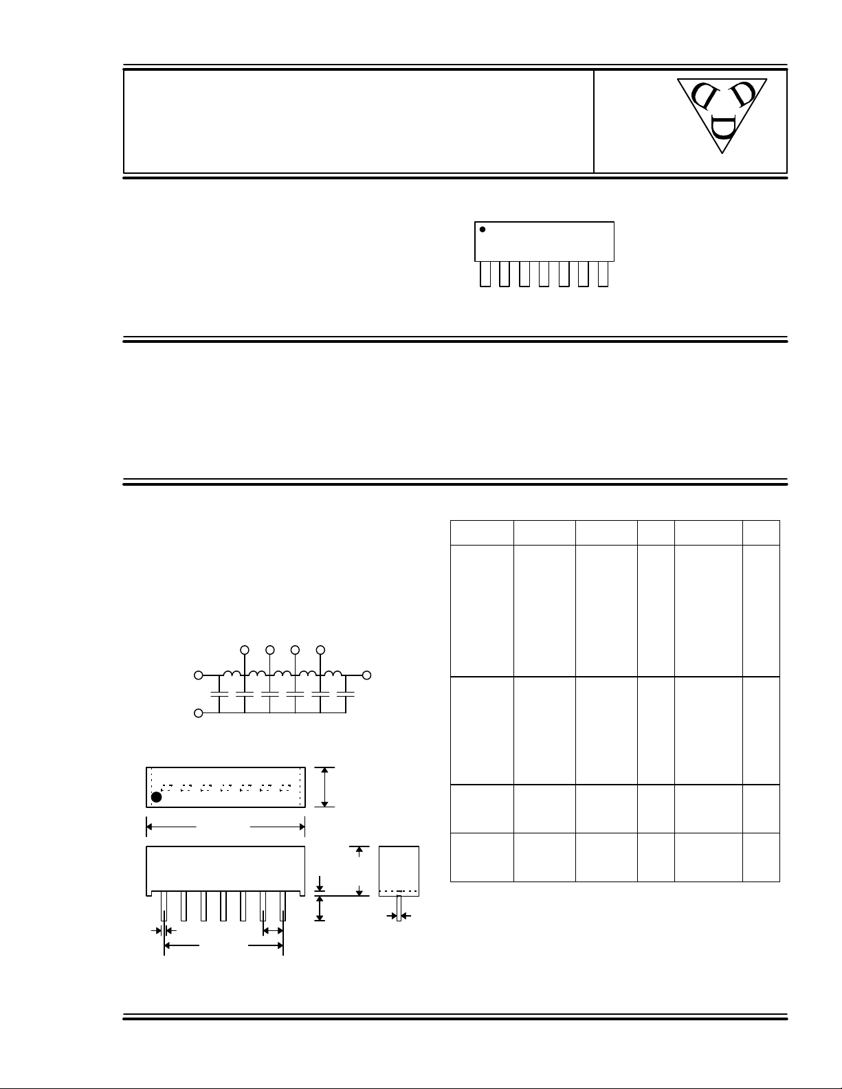
5-TAP SIP DELAY LINE
.800 MAX.
.020 TYP.
.600 TYP.
data
3
267
1
453
z = Impedance Code
TD/TR = 3
(SERIES 1505)
delay
devices, inc.
FEATURES PACKAGES
• 5 taps of equal delay increment
• Very narrow device (SIP package)
• Stackable for PC board economy
• Low profile
• Epoxy encapsulated
GND IN T5
T1 T2 T3 T4
• Meets or exceeds MIL-D-23859C
FUNCTIONAL DESCRIPTION
The 1505-series device is a fixed, single-input, five-output, passive delay
line. The signal input (IN) is reproduced at the outputs (T1-T5) in equal
increments. The delay from IN to T5 (TD) is given by the device dash
number. The characteristic impedance of the line is given by the letter
code that follows the dash number (See Table). The rise time (TR) of the line is 33% of TD, and the 3dB
bandwidth is given by 1.05 / TD.
SERIES SPECIFICATIONS
• Dielectric breakdown: 50 Vdc
• Distortion @ output: 10% max.
• Operating temperature: -55°C to +125°C
• Storage temperature: -55°C to +125°C
• Temperature coefficient: 100 PPM/°C
T1 T2 T3 T4
IN T5
GND
Functional Diagram
.200
.020
TYP.
MAX.
.250
MAX.
1 2 3 4 5 6 7
DASH NUMBER SPECIFICATIONS
Part
Number
1505-5A
1505-10A
1505-20A
1505-30A
1505-40A
1505-50A
1505-60A
1505-70A
1505-80A
1505-90A
1505-100A
1505-5B
1505-10B
1505-20B
1505-30B
1505-40B
1505-50B
1505-60B
1505-75B
1505-100B
1505-30C
1505-50C
1505-60C
1505-100C
1505-50G
1505-100G
1505-200G
1505-300G
T
(ns)
5.0 ± 1.0 1.0 ± 0.3
10.0 ± 1.0 2.0 ± 0.4
20.0 ± 1.5 4.0 ± 0.6
30.0 ± 2.0 6.0 ± 1.0
40.0 ± 2.5 8.0 ± 1.5
50.0 ± 3.0 10.0 ± 1.8
60.0 ± 3.0 12.0 ± 2.0
70.0 ± 3.5 14.0 ± 2.0
80.0 ± 4.0 16.0 ± 2.0
90.0 ± 5.0 18.0 ± 3.0
100 ± 5.0 20.0 ± 3.0
5.0 ± 1.0 1.0 ± 0.3
10.0 ± 1.0 2.0 ± 0.4
20.0 ± 1.5 4.0 ± 0.6
30.0 ± 2.0 6.0 ± 1.0
40.0 ± 2.5 8.0 ± 1.5
50.0 ± 3.0 10.0 ± 1.8
60.0 ± 3.0 12.0 ± 2.0
75.0 ± 3.5 15.0 ± 2.0
100 ± 5.0 20.0 ± 3.0
30.0 ± 2.0 6.0 ± 1.0
50.0 ± 3.0 10.0 ± 1.8
60.0 ± 3.0 12.0 ± 2.0
100 ± 5.0 20.0 ± 3.0
50.0 ± 3.0 10.0 ± 1.8
100 ± 5.0 20.0 ± 3.0
200 ± 10.0 40.0 ± 6.0
300 ± 15.0 60.0 ± 8.0
Delay per
D
Tap (ns)
1505-xxz
xx = Delay (TD)
PIN DESCRIPTIONS
IN Signal Input
T1-T5 Tap Outputs
GND Ground
T
Impedance
R
(ns)
2.0 50 0.6
3.0 50 0.6
6.0 50 0.7
9.0 50 0.7
12.0 50 0.9
15.0 50 1.0
18.0 50 1.2
21.0 50 1.4
24.0 50 1.6
27.0 50 1.8
30.0 50 2.0
2.0 100 0.7
3.0 100 0.7
6.0 100 1.0
9.0 100 1.5
12.0 100 1.8
15.0 100 2.0
18.0 100 2.0
24.0 100 2.5
30.0 100 2.5
9.0 200 2.5
15.0 200 3.0
18.0 200 3.5
30.0 200 6.0
15.0 500 5.0
30.0 500 15.0
60.0 500 21.0
90.0 500 29.0
(ΩΩ)
R
(ΩΩ)
DC
.100
.100
TYP.
MIN.
.010
TYP.
Package Dimensions
1997 Data Delay Devices
Doc #97024 DATA DELAY DEVICES, INC. 1
2/6/97 3 Mt. Prospect Ave. Clifton, NJ 07013
1505
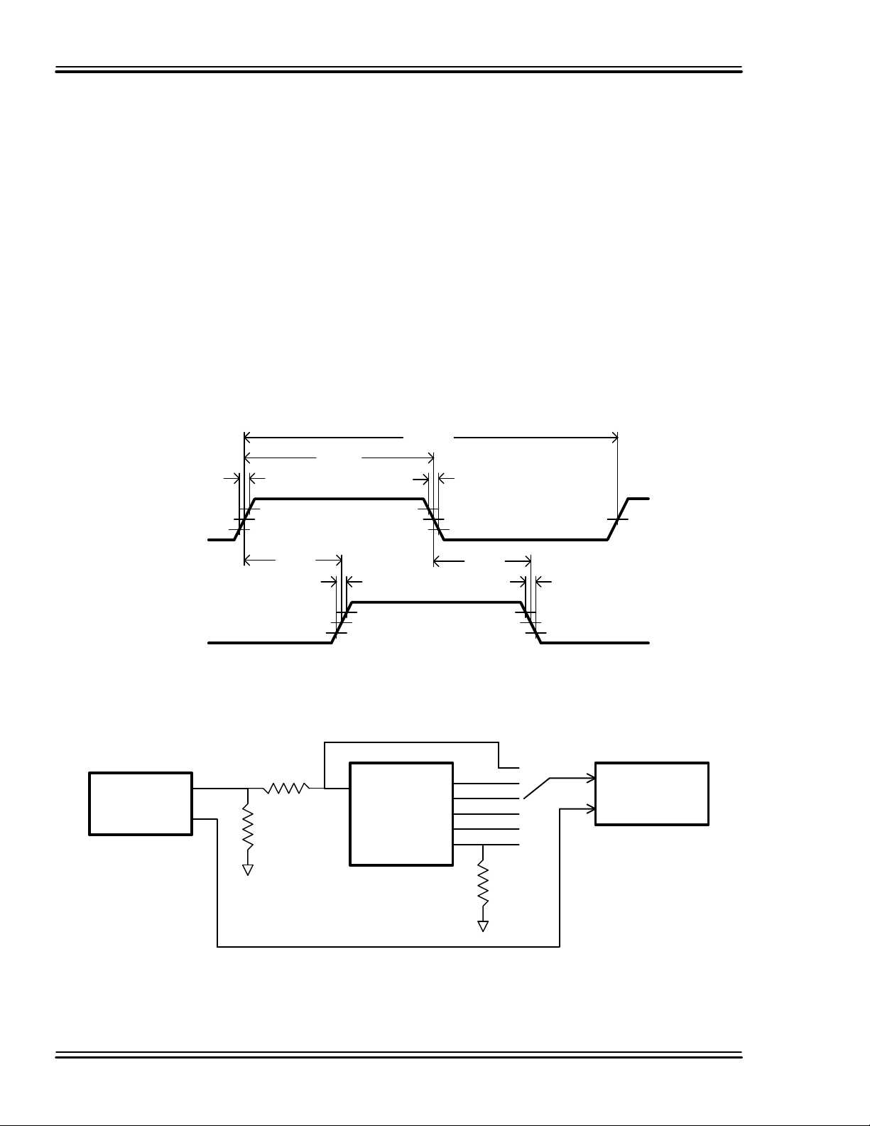
PASSIVE DELAY LINE TEST SPECIFICATIONS
10%
10%
50%
50%
90%
90%
50%
50%
10%
10%
90%
90%INT1
OUT
TRIGINTRIG
OSCILLOSCOPE
T2T3T4
T5
TEST CONDITIONS
INPUT: OUTPUT:
Ambient Temperature: 25oC ± 3oC R
Input Pulse: High = 3.0V typical C
Low = 0.0V typical Threshold: 50% (Rising & Falling)
Source Impedance: 50Ω Max.
Rise/Fall Time: 3.0 ns Max. (measured
at 10% and 90% levels)
Pulse Width (TD <= 75ns): PWIN = 100ns
Period (TD <= 75ns): PERIN = 1000ns
Pulse Width (TD > 75ns): PWIN = 2 x T
Period (TD > 75ns): PERIN = 10 x T
D
D
NOTE: The above conditions are for test only and do not in any way restrict the operation of the device.
PER
PW
IN
T
RISE
: 10MΩ
load
: 10pf
load
IN
T
FALL
INPUT
SIGNAL
OUTPUT
SIGNAL
PULSE
GENERATOR
R
50 Ω
V
IH
T
RISE
T
RISE
V
OH
Timing Diagram For Testing
IN
DEVICE UNDER
TEST (DUT)
RIN = R
OUT
= Z
LINE
T
FALL
V
IL
T
FALL
V
OL
R
OUT
Doc #97024 DATA DELAY DEVICES, INC. 2
2/6/97 Tel: 973-773-2299 Fax: 973-773-9672 http://www.datadelay.com
Test Setup
 Loading...