


DADD 1509J-40C, 1509J-10B, 1509-20D, 1509-20C, 1509-05B Datasheet
1509/1509J
Doc #01012 DATA DELAY DEVICES, INC. 1
11/2/01 3 Mt. Prospect Ave. Clifton, NJ 07013
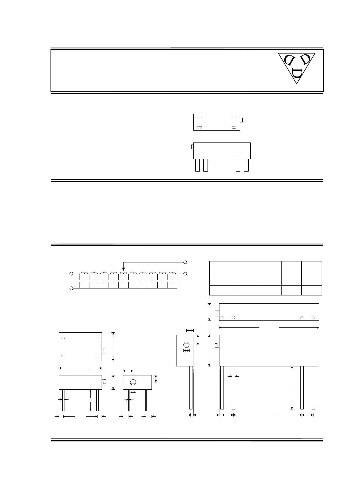
MECHANICALLY VARIABLE
DELAY LINE
(SERIES 1509 & 1509J)
FEATURES PACKAGES
• Ideal for “Set and Forget” applications
• Multi-turn adjustment screw
(1509: 20 turns, 1509J: 60 turns)
• Stackable for PC board economy
• Fits standard 14-pin DIP socket (1509)
• 20mil x 10mil flat leads (1509)
• #20 gauge leads (1509J)
• Resolution: As low as 0.15ns
• Dielectric breakdown: 50 Vdc
• Temperature coefficient: 200 PPM/°C
FUNCTIONAL DESCRIPTION
The 1509- and 1509J-series devices are mechanically variable, passive delay
lines. The signal input (IN) is reproduced at the tap output (TAP), shifted by an
amount which can be adjusted between 0 and TD, where TD is the device dash
number. The fixed output (OUT) reproduces the input, delayed by TD, and must
be terminated to match the characteristic impedance of the line, which is given
by the letter code that follows the dash number (See Table). The tap output is unbuffered. The 3dB
bandwidth of the line is given by 3.5 / TR, where TR is the rise time of the line (See Table).
SERIES SPECIFICATIONS
Functional Diagram
GND
IN
TAP
OUT
.250
Package Dimensions - 1509
.010
.170
.125
0.600
.080
.080
.300
.080
.080
.100
.460
0.760 MAX.
.375
3
4
.020
1
2
IN
GND TAP
OUT
.300
MAX.
1.750 MAX.
IN
G
TAPOUT
.565
MAX.
.032
Package Dimensions – 1509J
.125
.187
.750
1.200
.200
.200
.100
.062
.062
2001 Data Delay Devices
data
delay
devices,
inc.
3
1509
GND
IN OUT
TAP
1509J
GND IN OUT TAP
1509-xxz
1509J-xxz
xx = Max Delay (TD)
z = Impedance Code
PIN DESCRIPTIONS
IN Signal Input
TAP Variable Output
OUT Fixed Output
GND Ground
DASH NUMBER SPECIFICATIONS
Part
Number
Max Dly
(ns)
TR
(ns)
Imped
(ΩΩ)
RDC
(ΩΩ)
1509-05B 5 3 100 0.4
1509-20C 20 8 200 1.0
1509-20D 20 8 250 1.0
1509J-10B 10 4 100 0.8
1503J-40C 40 9 200 1.5
1509/1509J
Doc #01012 DATA DELAY DEVICES, INC. 2
11/2/01 Tel: 973-773-2299 Fax: 973-773-9672 http://www.datadelay.com
PASSIVE DELAY LINE TEST SPECIFICATIONS
TEST CONDITIONS
INPUT: OUTPUT:
Ambient Temperature: 25oC ± 3oC R
load
: 10MΩ
Input Pulse: High = 3.0V typical C
load
: 10pf
Low = 0.0V typical Threshold: 50% (Rising & Falling)
Source Impedance: 50Ω Max.
Rise/Fall Time: 3.0 ns Max. (measured
at 10% and 90% levels)
Pulse Width (TD <= 75ns): PWIN = 100ns
Period (TD <= 75ns): PERIN = 1000ns
Pulse Width (TD > 75ns): PWIN = 2 x T
D
Period (TD > 75ns): PERIN = 10 x T
D
NOTE: The above conditions are for test only and do not in any way restrict the operation of the device.
Timing Diagram For Testing
D
RISE
D
FALL
PER
IN
PW
IN
T
RISE
T
FALL
10%
10%
50%
50%
90%
90%
50%
50%
V
IH
V
IL
V
OH
V
OL
INPUT
SIGNAL
OUTPUT
SIGNAL
T
RISE
T
FALL
10%
10%
90%
90%INOUT
OUT
TRIGINTRIG
Test Setup
DEVICE UNDER
TEST (DUT)
OSCILLOSCOPE
PULSE
GENERATOR
50
Ω
R
OUT
R
IN
RIN = R
OUT
= Z
LINE
TAP
 Loading...