


DADD 1517-90C, 1517-80F, 1517-80C, 1517-75G, 1517-75E Datasheet
...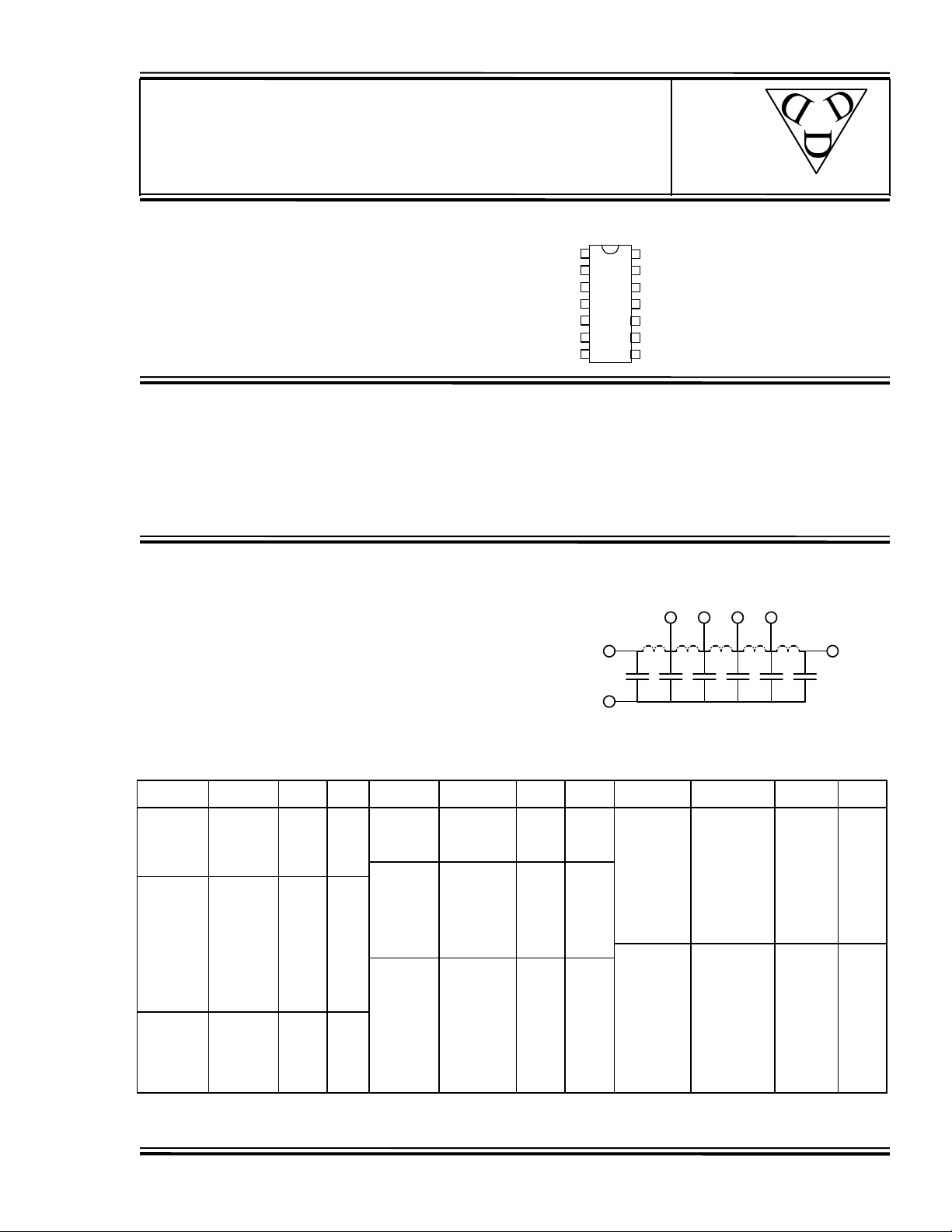
1517
5-TAP DIP DELAY LINE
data
3
z = Impedance Code
TD/TR = 3
(SERIES 1517)
delay
devices,
inc.
FEATURES PACKAGES
IN
• 5 taps of equal delay increment
• Delays as large as 300ns available
• Low DC resistance
• Standard 14-pin DIP package
• Epoxy encapsulated
• Meets or exceeds MIL-D-23859C
N/C
T2
N/C
T4
T5
GND
1
2
3
4
5
6
7
FUNCTIONAL DESCRIPTION
The 1517-series device is a fixed, single-input, five-output, passive delay
line. The signal input (IN) is reproduced at the outputs (T1-T5) in equal
increments. The delay from IN to T5 (TD) is given by the device dash
number. The characteristic impedance of the line is given by the letter
code that follows the dash number (See Table). The rise time (TR) of the
line is 33% of TD, and the 3dB bandwidth is given by 1.05 / TD.
N/C
14
T1
13
N/C
12
T3
11
N/C
10
N/C
9
N/C
8
1517-xxz
xx = Delay (TD)
PIN DESCRIPTIONS
IN Signal Input
T1-T5 Tap Outputs
GND Ground
SERIES SPECIFICATIONS FUNCTIONAL DIAGRAM
• Dielectric breakdown: 50 Vdc
• Distortion @ output: 10% max.
• Operating temperature: -55°C to +125°C
• Storage temperature: -55°C to +125°C
• Temperature coefficient: 100 PPM/°C
IN T5
T1 T2 T3 T4
Part
Number
1517-10A
1517-15A
1517-20A
1517-30A
1517-40A
1517-5B
1517-10B
1517-15B
1517-20B
1517-25B
1517-30B
1517-40B
1517-50B
1517-60B
1517-75B
1517-10C
1517-20C
1517-30C
1517-40C
1517-50C
1517-60C
Delay
(ns)
10.0 ± 1.0
15.0 ± 1.0
20.0 ± 1.0
30.0 ± 1.5
40.0 ± 2.0
5.0 ± 1.0
10.0 ± 1.0
15.0 ± 1.0
20.0 ± 1.0
25.0 ± 1.3
30.0 ± 1.5
40.0 ± 2.0
50.0 ± 2.5
60.0 ± 3.0
75.0 ± 3.8
10.0 ± 1.0
20.0 ± 1.0
30.0 ± 1.5
40.0 ± 2.0
50.0 ± 2.5
60.0 ± 3.0
Imped
2001 Data Delay Devices
DASH NUMBER SPECIFICATIONS
RDC
(ΩΩ)
(ΩΩ)
50 0.6 1517-80C
50 0.6 1517-90C
50 0.7 1517-120C
50 0.7 1517-150C
50 0.9 1517-25D
100 0.5 1517-37D
100 0.7 1517-50D
100 0.7 1517-60D
100 0.9 1517-75D
100 1.0 1517-100D
100 1.5 1517-150D
100 1.8 1517-15E
100 2.0 1517-30E
100 2.0 1517-50E
100 2.5 1517-60E
200 1.5 1517-75E
200 2.0 1517-90E
200 2.5 1517-120E
200 3.0 1517-130E
200 3.0 1517-180E
200 3.5 1517-220E
Part
Number
Delay
(ns)
80.0 ± 4.0
90.0 ± 4.5
120.0 ± 6.0
150.0 ± 7.5
25.0 ± 1.3
37.0 ± 1.9
50.0 ± 2.5
60.0 ± 3.0
75.0 ± 3.8
100.0 ± 5.0
150.0 ± 7.5
15.0 ± 1.0
30.0 ± 1.5
50.0 ± 2.5
60.0 ± 3.0
75.0 ± 3.8
90.0 ± 4.5
120.0 ± 6.0
130.0 ± 6.5
180.0 ± 9.0
220.0 ± 11.0
GND
Imped
RDC
(ΩΩ)
200 3.5 1517-20F
200 5.0 1517-40F
200 5.0 1517-60F
200 8.0 1517-80F
250 2.5 1517-100F
250 3.0 1517-120F
250 3.5 1517-160F
250 4.0 1517-180F
250 4.0 1517-240F
250 5.0 1517-300F
250 8.5 1517-25G
300 2.5 1517-50G
300 3.0 1517-75G
300 4.0 1517-100G
300 4.0 1517-125G
300 4.5 1517-150G
300 5.5 1517-200G
300 8.0 1517-225G
300 9.0 1517-300G
300 11.0
300 13.0
(ΩΩ)
Part
Number
Delay
(ns)
20.0 ± 1.0
40.0 ± 2.0
60.0 ± 3.0
80.0 ± 4.0
100.0 ± 5.0
120.0 ± 6.0
160.0 ± 8.0
180.0 ± 9.0
240.0 ± 12.0
300.0 ± 15.0
25.0 ± 1.3
50.0 ± 2.5
75.0 ± 3.8
100.0 ± 5.0
125.0 ± 6.3
150.0 ± 7.5
200.0 ± 10.0
225.0 ± 11.3
300.0 ± 15.0
Imped
(ΩΩ)
400 4.5
400 5.0
400 5.0
400 8.0
400 9.0
400 10.0
400 13.0
400 14.0
400 19.0
400 23.0
500 3.0
500 5.0
500 8.0
500 15.0
500 9.0
500 13.0
500 21.0
500 23.0
500 29.0
RDC
(ΩΩ)
Doc #01007 DATA DELAY DEVICES, INC. 1
10/30/01 3 Mt. Prospect Ave. Clifton, NJ 07013
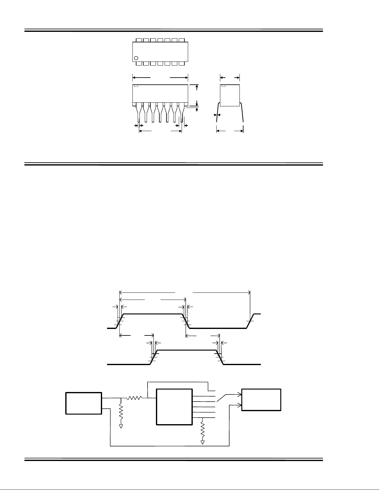
1517
.780 MAX.
1 2 3 4 5 6 7
.015 TYP.
.070 MAX.
Package Dimensions
10%
10%
50%
50%
90%
90%
50%
50%
10%
10%
90%
90%INT1
OUT
TRIGINTRIG
OSCILLOSCOP
T2T3T4
T5
814 13 12 11 10 9
Lead Material:
Nickel-Iron alloy 42
TIN PLATE
.280
MAX.
See
Table
.018
TYP.
.600±.010
6 Equal spaces
each .100±.010
Non-Accumulative
.010±.002
.350
MAX.
PASSIVE DELAY LINE TEST SPECIFICATIONS
TEST CONDITIONS
INPUT: OUTPUT:
Ambient Temperature: 25oC ± 3oC R
Input Pulse: High = 3.0V typical C
Low = 0.0V typical Threshold: 50% (Rising & Falling)
Source Impedance: 50Ω Max.
Rise/Fall Time: 3.0 ns Max. (measured
at 10% and 90% levels)
Pulse Width (TD <= 75ns): PWIN = 100ns
Period (TD <= 75ns): PERIN = 1000ns
Pulse Width (TD > 75ns): PWIN = 2 x T
Period (TD > 75ns): PERIN = 10 x T
D
D
NOTE: The above conditions are for test only and do not in any way restrict the operation of the device.
PER
PW
IN
T
RISE
INPUT
SIGNAL
OUTPUT
SIGNAL
V
IH
D
RISE
T
RISE
V
Timing Diagram For Testing
OH
: 10MΩ
load
: 10pf
load
IN
T
FALL
D
FALL
V
IL
T
FALL
V
OL
R
IN
PULSE
GENERATOR
50
Ω
DEVICE UNDER
TEST (DUT)
RIN = R
OUT
= Z
LINE
R
OUT
Test Setup
Doc #01007 DATA DELAY DEVICES, INC. 2
10/30/01 Tel: 973-773-2299 Fax: 973-773-9672 http://www.datadelay.com
 Loading...