


HP L1902 Service Manual
-
SERVICE MANUAL
19” LCD Monitor
L1902
THESE DOCUMENTS ARE FOR REPAIR SERVICE INFORMATION ONLY. EVERY REASONABLE EFFORT HAS BEEN MADE TO ENSURE THE ACCURACY OF THIS MANUAL; WE CANNOT GUARANTEE THE ACCURACY OF THIS INFORMATION AFTER THE DATE OF PUBLICATION AND DISCLAIMS RELIABILITY FOR CHANGES, ERRORS OR OMISSIONS.
MANUFACTURE DATA Feb-29-2004
Page 1 of 69

|
|
|
HP L1902 Service Manual |
|
|
Table of Contents |
|
Table of Contents ---------------------------------------------------------------------------------- |
02 |
||
Revision List |
---------------------------------------------------------------------------------------- |
04 |
|
1.Product Feature --------------------------------------------------------------------- |
05 |
||
2 LCD Monitor Description --------------------------------------------------------------- |
05 |
||
3 Operation Instructions -------------------------------------------------------------------- |
06 |
||
3.1 |
General |
Instructions ------------------------------------------------------------------ |
06 |
3.2 |
Control |
Button ------------------------------------------------------------------------- |
06 |
3.3 |
Adjusting The Picture ---------------------------------------------------------------- |
07 |
|
4. Input/Output Specification ---------------- --------------------------------------------------- |
08 |
||
4.1 |
Input Signal Connector ------------------------------------------------------------------ |
08 |
|
4.1.1 Analog D-SUB Connector ---------------------------------------------------------- |
08 |
||
4.2 |
Factory Preset Display Modes -------------------------------------------------------- |
09 |
|
4.3 |
Power Supply Requirements ---------------------------------------------------------- |
09 |
|
|
4.3.1 Input/Output Requirements ------------------------------------------------------ |
09 |
|
|
4.3.2 Inverter Max Brightness ----------------------------------------------------------- |
10 |
|
|
4.3.3 Inverter Min Brightness ------------------------------------------------------------ |
10 |
|
5.Panel Specification (LG E03/AU EN04) ------------------------------------------------ |
11 |
||
5.1 |
General Feature ------------------------------------------------------------------------- |
11 |
|
5.2 |
Optical |
Characteristics --------------------------------------------------------------- |
12 |
6. Block Diagram ----------------------------------------------------------------------------------- |
14 |
||
6.1 |
Monitor Exploded View ---------------------------------------------------------------- |
14 |
|
6.2 |
Software Flow Chart --------------------------------------------------------------------- |
15 |
|
|
|
Page 2 of 69 |
|

|
HP L1902 Service Manual |
6.3 Electrical Block Diagram ---------------------------------------------------------------- |
16 |
6.3.1 Scalar Board ---------------------------------------------------------------------- |
16 |
6.3.2 Inverter/Power Board ----------------------------------------------------------- |
17 |
7. Schematic ----------------------------------------------------------------------------------------- |
19 |
7.1 Scalar Board ---------------------------------------------------------------------------- |
19 |
7.2 Inverter/Power Board -------------------------------------------------------------- |
25 |
7.3 Key Pad Board ------------------------------------------------------------------------- |
26 |
8. PCB Layout -------------------------------------------------------------------------------------- |
27 |
8.1 Main Board ----------------------------------------------------------------------------- |
27 |
8.2 Inverter/Power Board ---------------------------------------------------------------- |
30 |
8.3 Keypad Board ------------------------------------------------------------------------- |
25 |
9. Maintainability ----------------------------------------------------------------------------------- |
30 |
9.1 Equipments and Tools Requirements --------------------------------------------- |
30 |
9.2 Trouble Shooting ----------------------------------------------------------------------- |
31 |
9.2.1 Main Board ------------------------------------------------------------------ |
31 |
9.2.2 Power/Inverter Board ------------------------------------------------------- |
33 |
9.2.3 Key Pad Board ----------------------------------------------------------------- |
35 |
10. White-Balance, Luminance Adjustment ----------------------------------------------- |
36 |
11. EDID Content ----------------------------------------------------------------------------------- |
37 |
12. BOM List ---------------------------------------------------------------------------------- |
38 69 |
12.1 T980KGLHKHHPN ------------------------------------------------------ |
38 53 |
12.2 T980KAXDKHHPN ------------------------------------------------------ |
53 69 |
Page 3 of 69 |
|
|
|
HP L1902 Service Manual |
|
|
|
Revision List |
|
|
|
|
|
Revision |
Date |
Change Description |
|
A00 |
May-31-04 |
Add Panel spec and BOM of AU Panel model |
|
|
|
|
|
|
|
|
|
|
|
|
|
|
|
|
|
|
|
|
|
|
|
|
|
|
|
|
|
|
|
|
|
|
|
|
|
|
|
|
|
|
|
|
|
|
|
|
|
|
|
|
|
|
|
|
|
|
|
|
|
|
|
|
|
|
|
|
|
|
|
|
|
|
|
|
|
|
|
|
|
|
|
|
|
|
|
|
|
|
|
|
|
|
|
|
|
|
|
|
|
|
|
|
|
|
|
|
|
|
|
|
|
|
|
|
|
|
|
|
|
|
|
|
|
Page 4 of 69

HP L1902 Service Manual
1.PRODUCT FEATURE
48.18cm(19”) a-si TFT Active matrix LCD panel, 0.294mm dot pitch Scalar chipset : gmZAN3SL ( or MST9111B)
Microprocessor controlled scan technology 16 factory presets, 20 new modes
Vertical refresh rate 50Hz to 75Hz; Horizontal frequency 30kHz to 83kHz Resolutions: 640 x 480 up to 1280 x 1024
Power Internal AC100V-240V (+/-10%) Tilt -5° to 20°
CE mark TCO 03 mark
VESA DPMS compliant
VESA DDC2B compliant and DDC/CI interface.
2. LCD MONITOR DESCRIPTION
The LCD Monitor will contain main board, power board, key board and which house the flat panel control logic, brightness control logic and DDC.
The power board will provide AC to DC Inverter voltage to drive the backlight of panel and the main board chips each voltage.
Monitor Block Diagram
CCFT Drive. |
Flat Panel and |
|
CCFL backlight |
||
|
||
|
|
Power Board |
|
|
Main Board |
|
|
|
||
|
|
|
|
RS232 Connector |
||||
|
|
|
|
|
|
|
|
|
|
|
|
|
|
|
|
|
For white balance |
|
|
|
|
|
|
|
|
adjustment in |
|
|
|
|
|
|
|
|
factory mode |
|
|
|
Keyboard |
|
|
|
||
|
|
|
|
|
|
|
||
AC-IN |
|
|
|
|
|
|
|
|
|
|
|
|
|
|
|
|
|
|
|
|
HOST Computer |
|
Video signal, DDC |
|||
100V-240V |
|
|
|
|
||||
Page 5 of 69
HP L1902 Service Manual
3. OPERATION INSTRUCTIONS
3.1 General Instructions
Press the power button to turn the monitor on or off. The other control buttons are located at front panel of the monitor. By changing these settings, the picture can be adjusted
to your personal performance.
-The power cord should be connected and insert to adaptor.
-Connect the video cable from the monitor to the computer VGA card.
-Press the power button to turn on the monitor, the power indicator will light up to Green.
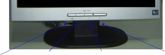
3.2Control Buttons
-Power Button:
When pressed, the monitor enters the off mode, and the LED turns blank. Press again to restore normal status.
-(Down/ Auto) and + (Up) Button:
The -/+ Button is browse OSD key. Press a select into adjustment.
The Auto Adjust Key is used to automatically set the H Position, V Position, Clock and Phase.
- Select Key:
Select key is into OSD sub-menu hot key when OSD turn on.
-Power Indicator:
Green — Power On mode. Amber — Power Saving mode. Blank — Power Off Mode.
CONTROL BUTTONS
Select Button |
Down / Auto Button |
Up Button |
On/Off Switch |
Page 6 of 69
HP L1902 Service Manual
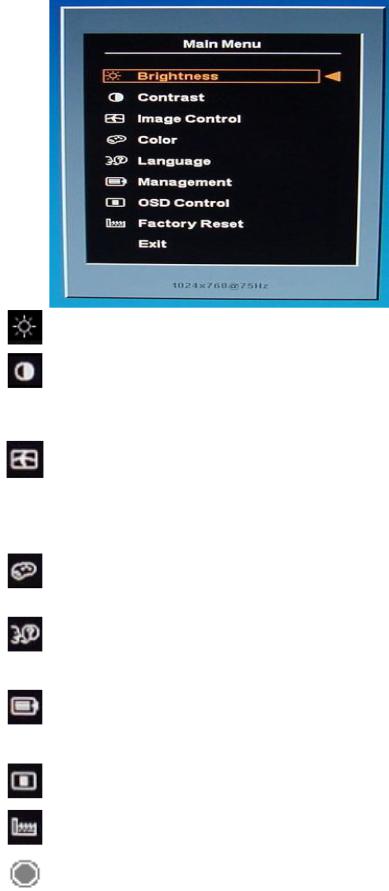
3.3 Adjust The Picture
1. |
|
Brightness |
Adjust the brightness. |
|
|
||
|
|
|
|
2. |
|
Contrast |
Adjust the contrast |
|
|
|
|
|
|
|
Adjust the: |
|
|
|
z Auto Adjustment: Adjusts the main settings and produces a |
|
|
|
stable, centered image. |
3. |
|
Image Control |
z H-Position: horizontal position of the screen image. |
|
|
z V-Position: vertical position of the screen image. |
|
|
|
|
|
|
|
|
z Clock: frequency of the pixel clock to minimize vertical bar. |
|
|
|
z Phase: phase value to minimize horizontal jitters. |
|
|
|
|
|
|
|
z 9300K: recall 9300K color |
|
|
|
z 6500K: recall 6500K color |
3. |
|
Color |
z SRGB: recall SRGB color |
|
|
|
z Custom Color: adjusts the color tint of white, and the red, |
|
|
|
green, and blue (RGB) mix for colors. |
4. |
|
Language |
Shows the language of the OSD window. |
|
|
|
|
5. |
|
|
z Power Saver: enable/disable power saving |
|
|
z Power On Recall: enable/disable power recall |
|
|
|
|
|
|
|
Management |
z Mode Display: enable/disable mode display |
|
|
|
z Sleep Timer: set sleep timer |
|
|
|
z Basic Menu: set to basic menu |
|
|
|
|
6. |
|
OSD Control |
OSD (on Screen Display) settings: adjusts the H/V position, |
|
timeout, On Screen Display window. |
||
|
|
|
|
|
|
|
|
7. |
|
Factory Reset |
Resets the display to original factory settings for color, brightness, |
|
phase, and clock. |
||
|
|
|
|
8. |
|
Exit |
Exit the current OSD window. |
|
|
|
|
Page 7 of 69
HP L1902 Service Manual
4. Input/Output Specification
4.1 Input Signal Connector
4.1.1 Analog D-SUB Connector
PIN |
MNEMONIC |
SIGNAL |
1 |
RV |
Red Video |
2 |
GV |
Green Video |
3 |
BV |
Blue Video |
4 |
NC |
None |
5 |
GND |
Ground (DDC Return) |
6 |
RG |
Red GND |
7 |
GG |
Green GND |
8 |
BG |
Blue GND |
9 |
+5 V |
+5 V (from PC) |
10 |
SG |
Sync Ground |
11 |
NC |
None |
12 |
SDA |
DDC Data |
13 |
HS |
Horizontal Sync |
14 |
VS |
Vertical Sync |
15 |
SCL |
DDC Clock |
VGA connector layout
PIN 1 |
PIN 5 |
PIN 11 |
|
Page 8 of 69
HP L1902 Service Manual
4.2 Factory Preset Display Modes
|
Preset |
Pixel |
|
Horz |
|
Horz |
Vert Freq |
Vert |
Pixel Clk |
Source |
|||
|
Format |
|
Freq (KHz) |
|
Polarity |
(Hz) |
Polarity |
(MHz) |
|||||
|
|
|
|
|
|
||||||||
|
|
|
|
|
|
|
|
|
|
|
|
|
|
|
1 |
640 x 480 |
|
31.469 |
|
- |
59.940 |
- |
25.175 |
VGA |
|||
|
2 |
640 x 480 |
|
37.861 |
|
- |
72.809 |
- |
31.500 |
VESA |
|||
|
3 |
640 x 480 |
|
37.500 |
|
- |
75.000 |
- |
31.500 |
VESA |
|||
|
4 |
720 x 400 |
|
31.469 |
|
- |
70.087 |
+ |
28.322 |
VGA |
|||
|
5 |
800 x 600 |
|
37.879 |
|
+ |
60.317 |
+ |
40.000 |
VESA |
|||
|
6 |
800 x 600 |
|
48.077 |
|
+ |
72.188 |
+ |
50.000 |
VESA |
|||
|
7 |
800 x 600 |
|
46.875 |
|
+ |
75.000 |
+ |
49.500 |
VESA |
|||
|
8 |
832 x 624 |
|
49.726 |
|
± |
74.551 |
± |
57.284 |
MAC |
|||
|
9 |
1024 x 768 |
|
48.363 |
|
- |
60.004 |
- |
65.000 |
VESA |
|||
|
10 |
1024 x 768 |
|
56.476 |
|
- |
70.069 |
- |
75.000 |
VESA |
|||
|
11 |
1024 x 768 |
|
60.023 |
|
+ |
75.029 |
+ |
78.750 |
VESA |
|||
|
12 |
1152 x 870 |
|
68.68 |
|
- |
75.06 |
- |
100.000 |
Mac |
|||
|
13 |
1152 x 900 |
|
71.71 |
|
- |
76.05 |
- |
105.561 |
Sun |
|||
|
14 |
1280 x 1024 |
|
63.98 |
|
+ |
60.02 |
+ |
108.000 |
VESA |
|||
|
15 |
1280 x 1024 |
|
79.97 |
|
+ |
75.02 |
+ |
135.000 |
VESA |
|||
4.3 Power Supply Requirements |
|
|
|
|
|
|
|||||||
4.3.1 Input / Output Requirements |
|
|
|
|
|
|
|||||||
|
|
|
PARAMETER |
|
|
|
|
RANGE |
|
|
|
|
|
|
|
|
|
|
|
|
|
|
|
||||
|
|
AC Input Voltage |
|
90 to 264V |
|
|
|
|
|
||||
|
|
|
|
|
|
|
|
|
|
||||
|
|
AC Input Frequency |
|
47 to 63 Hz |
|
|
|
|
|
||||
|
|
|
|
|
|
|
|
|
|
||||
|
|
AC Input Current |
|
1.5A MAX |
|
|
|
|
|
||||
|
|
|
|
|
|
|
|
||||||
|
|
Inrush Current |
|
60A MAX AT 264VAC COLD START |
|
|
|
||||||
|
|
|
|
|
|
|
|||||||
|
|
Leakage Current |
|
3.5 mA MAX and less than 0.25mA at 100Vac |
|
|
|||||||
|
|
|
|
|
|
|
|
|
|||||
|
|
Output voltage / current |
|
12V / 3.5A , 5V / 1.5A |
|
|
|
|
|||||
|
|
|
|
|
|
|
|
|
|
||||
|
|
Output power |
|
45W Max |
|
|
|
|
|
||||
|
|
|
|
|
|
|
|
|
|
|
|||
|
|
Efficiency |
|
>80% |
|
|
|
|
|
|
|||
|
|
|
|
|
|
|
|
|
|||||
|
|
Saving Mode |
|
<2W Max @5V/0.1A , 12V/0A |
|
|
|
|
|||||
|
|
|
|
|
|
|
|
|
|
|
|
|
|
Page 9 of 69
HP L1902 Service Manual
4.3.2 Inverter Max Brightness
(Vadj:4.5v), LOAD=100KΩX4 (ROOM TEMPERATURE 25 ±4 )
ITEM |
SYMBOL |
MIN. |
TYP. |
MAX. |
UNIT |
REMARK |
Input voltage |
Vin |
10.8 |
12 |
13.2 |
V |
|
Input current |
Iin |
|
1700 |
1870 |
mA |
FOR 4LOAD |
Output Current |
Iout |
6 |
6.5 |
7 |
mA |
FOR 1 LOAD |
Frequency |
F |
40 |
50 |
60 |
KHZ |
FOR 1 LOAD |
|
|
|||||
H.V open |
Vopen |
1350 |
1550 |
1750 |
Vrms |
NO LOAD |
|
|
|
|
|
|
|
H.V Load |
Vload |
550 |
650 |
750 |
Vrms |
RL=100KΩ |
|
|
|
|
|
|
|
Protect delay time |
PDT |
0.4 |
1 |
4 |
Sec |
|
|
|
|
|
|
|
|
4.3.3 Inverter Min Brightness
(Vadj:0.0v), LOAD=100KΩX4 (ROOM TEMPERATURE 25 ±4 )
ITEM |
SYMBOL |
MIN. |
TYP. |
MAX. |
UNIT |
REMARK |
input voltage |
Vin |
10.8 |
12 |
13.2 |
V |
|
input current |
Iin |
-- |
500 |
550 |
mA |
FOR 4 LOAD |
Output Current |
Iout |
3 |
3.5 |
4 |
mA |
FOR 1 LOAD |
Frequency |
F |
40 |
50 |
60 |
KHZ |
FOR 1 LOAD |
|
|
|||||
H.V open |
Vopen |
1350 |
1550 |
1750 |
Vrms |
NO LOAD |
|
|
|
|
|
|
|
H.V Load |
Vload |
250 |
350 |
450 |
Vrms |
RL=100KΩ |
|
|
|
|
|
|
|
Page 10 of 69
HP L1902 Service Manual
5. PANEL SPECIFICATION
5.1 General Feature
LG LM190E03
Active Screen Size |
|
19.0 inches(481.84mm) diagonal |
|||
Outline Dimension |
|
404.2(H) 330.0(V) 20.0(D) mm(Typ.) |
|||
Pixel Pitch |
|
0.098*RGB(H) 0.294(V)mm |
|||
Pixel Format |
|
1280 horizontal By 1024 vertical Pixels. RGB stripe arrangement |
|||
Interface |
|
LVDS 2Port |
|
|
|
Color Depth |
|
16.2M colors |
|
|
|
Luminance, White |
|
250 cd/m²(Center 1 Point ,Typ) |
|||
Viewing Angle(CR>10) |
|
Viewing Angle Free[R/L 140(Typ.), U/D 140(Typ.)] |
|||
Power Consumption |
|
Total 20.82Watt(Typ.),(2.22Watt @VLCD, 18.60 @ [Lamp=6.5mA]) |
|||
Weight |
|
2500g(Typ.) |
|
|
|
Display Operating Mode |
|
Transmissive mode, normally White |
|||
Surface treatments |
|
Hard coating(3H), Anti-glare treatment of the front polarizer |
|||
AU M190EN04 |
|
|
|
|
|
ITEM |
|
Unit |
Specifications |
|
|
Screen Diagonal |
|
[mm] |
480(19.0") |
|
|
Active Area |
|
[mm] |
376.32(H) 301.056(V) |
|
|
Pixels H V |
|
|
1280( 3) 1024 |
|
|
Pixel Pitch |
|
[mm] |
0.294(per one triad) 0.294 |
|
|
Pixel Arrangement |
|
|
R.G.B Vertical Stripe |
|
|
Display Mode |
|
|
Normally White |
|
|
White Luminance |
|
[cd/m²] |
250(center, Typ)@7mA |
|
|
Contrast Ratio |
|
|
450:1(Typ.) |
|
|
Optical Response Time |
|
[msec] |
16ms(Typ) |
|
|
Color Saturation |
|
|
72% NTSC |
|
|
Nominal input Voltage VDD |
|
[Volt] |
+5V |
|
|
Power Consumption |
|
[Watt] |
28W(Typ.)(w/o inverter, All back pattern) |
|
|
(VDD line + CCFL line) |
|
|
|||
|
|
|
|
||
Weight |
|
[Grams] |
2700(TBD) |
|
|
Physical Size |
|
[mm] |
396(H) 324(V) 18(D)(Typ) |
|
|
Electrical interface |
|
|
R.G.B data, Clock |
|
|
Support Color |
|
|
262k colors(RGB 6-bit data) |
|
|
Surface Treatment |
|
|
Anti-Glare,Hard Coating,3H |
|
|
Temperature Range |
|
[ ] |
0 to +50 |
|
|
Operating |
|
|
|||
|
[ ] |
-20 to +60 |
|
||
Storage(Shipping) |
|
|
|||
|
|
|
|
||
TCO compliance |
|
|
Meet TCO'03 regulation |
|
|
Page 11 of 69
HP L1902 Service Manual
5.2 Optical Characteristics
LG LM190E03
Ta= 25°C, VLCD=5.0V, fV=60Hz ,Dclk=54MHz
Parameter |
Symbol |
|
Values |
|
Units |
Notes |
||
Min |
Typ |
Max |
||||||
|
|
|
|
|
||||
Contrast Ratio |
|
CR |
300 |
500 |
- |
|
1 |
|
Surface Luminance, white |
LWH |
200 |
250 |
- |
cd/m² |
2 |
||
Luminance Variation |
δWHITE 5P |
|
|
1.3 |
|
3 |
||
Response time |
Rise Time |
TrR |
- |
4 |
6 |
ms |
4 |
|
Decay Time |
TrD |
- |
12 |
24 |
ms |
4 |
||
|
||||||||
|
RED |
Rx |
|
0.639 |
|
|
|
|
|
Ry |
|
0.342 |
|
|
|
||
|
|
|
|
|
|
|||
|
GREEN |
Gx |
|
0.297 |
|
|
|
|
Color |
Gy |
Typ |
0.615 |
Typ |
|
|
||
|
|
|
||||||
Coordinates |
BLUE |
Bx |
-0.03 |
0.146 |
+0.03 |
|
|
|
|
By |
|
0.068 |
|
|
|
||
|
|
|
|
|
|
|||
|
WHITE |
Wx |
|
0.313 |
|
|
|
|
|
Wy |
|
0.329 |
|
|
|
||
|
|
|
|
|
|
|||
Viewing Angle(CR>5) |
|
|
|
|
|
|
||
|
x axis, right(=0°) |
r |
70 |
80 |
|
degree |
5 |
|
|
x axis, right(=180°) |
l |
70 |
80 |
|
|
|
|
|
y axis, up(=90°) |
u |
70 |
80 |
|
|
|
|
|
y axis, down(=270°) |
d |
70 |
80 |
|
|
|
|
Viewing Angle(CR>10) |
|
|
|
|
|
|
||
|
x axis, right(=0°) |
r |
60 |
70 |
|
degree |
5 |
|
|
x axis, right(=180°) |
l |
60 |
70 |
|
|
|
|
|
y axis, up(=90°) |
u |
60 |
70 |
|
|
|
|
|
y axis, down(=270°) |
d |
60 |
70 |
|
|
|
|
Gray Scale |
|
|
|
2.2 |
|
|
6 |
|
Page 12 of 69
HP L1902 Service Manual
AU M190EN04
ITEM |
Unit |
Condition |
Min. |
Typ. |
Max. |
||
|
|
Horizontal (Right) |
65 |
70 |
|
||
|
|
CR=10 |
|
– |
|||
|
|
|
65 |
70 |
|||
|
|
(Left) |
|
|
|||
Viewing Angle |
[degree] |
|
|
|
|
||
Vertical |
(Up) |
65 |
70 |
|
|||
|
|
CR=10 |
|
– |
|||
|
|
|
60 |
65 |
|||
|
|
(Down) |
|
|
|||
|
|
|
|
|
|
||
Contrast ratio |
|
Normal Direction |
250 |
450 |
– |
||
Response Time |
|
Raising Time |
– |
4 |
5 |
||
[msec] |
Falling Time |
– |
12 |
20 |
|||
(Note 1) |
|||||||
|
Rising + Failing |
– |
16 |
25 |
|||
|
|
||||||
|
|
Red x |
|
0.604 |
0.634 |
0.664 |
|
|
|
Red y |
|
0.324 |
0.354 |
0.384 |
|
Color/Chromaticity |
|
Green X |
|
0.27 |
0.3 |
0.33 |
|
Coordinates(CIE) |
|
Green y |
|
0.585 |
0.615 |
0.645 |
|
|
|
Blue x |
|
0.108 |
0.138 |
0.168 |
|
|
|
Blue y |
|
0.047 |
0.077 |
0.107 |
|
Color Coordinates |
|
White x |
|
0.28 |
0.31 |
0.34 |
|
(CIE)White |
|
White y |
|
0.3 |
0.33 |
0.36 |
|
White Luminance@ |
[cd/m²] |
|
|
200 |
250 |
– |
|
CCFL 7mA(Center) |
|
|
|||||
|
|
|
|
|
|
||
|
|
|
|
|
|
|
|
Luminance Uniformity |
[%] |
|
|
70 |
75 |
– |
|
(Note 2) |
|
|
|||||
|
|
|
|
|
|
||
|
|
|
|
|
|
|
|
Closs talk (in 75Hz) |
[%] |
|
|
– |
– |
1.5 |
|
(Note 3) |
|
|
|||||
|
|
|
|
|
|
||
|
|
|
|
|
|
|
|
Page 13 of 69
HP L1902 Service Manual
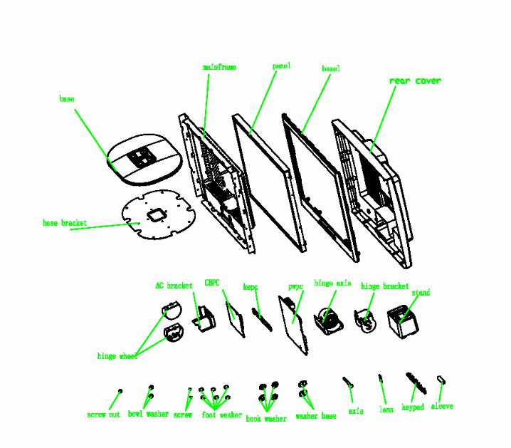
6. Block Diagram
6.1 Monitor Exploded View
Page 14 of 69
HP L1902 Service Manual
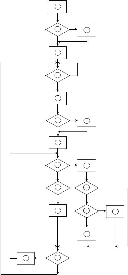
6.2 Software Flow Chart
1
2 Y 3
N
4
5 N
Y
6
7 N 8
Y
9
10 |
N |
11 |
|
|
Y |
|
|
|
|
N 12 |
|
13 |
N |
|
Y |
Y |
|
|
|
14 |
|
15 |
N |
16 |
|
|
Y |
|
|
|
|
17 |
|
|
1)MCU initialize.
2)Is the eeprom blank?
3)Program the eeprom by default values.
4)Get the PWM value of brightness from eeprom. Check the pin PANEL1 and PANEL2 to tell which panel to get with it.
5)Is the power key pressed?
6)Clear all global flags.
7)Are the AUTO and SELECT keys pressed?
8)Enter factory mode.
9)Saving the power key status into eeprom. Turn on the LED and set it to green color. Scalar initializes.
10)In standby mode?
11)Update the lifetime of back light.
12)Check the analog and digital port, are there any signals coming?
13)Does the scalar send out a interrupt request?
14)Wake up the scalar.
15)Are there any signals coming from analog or digital port?
16)Display " No Input Signal " message. And go into standby mode after the message disappear.
17)Program the scalar to be able to show the coming mode.
18)Process the OSD display.
19)Read the keyboard. Is the power key pressed?
18 |
N 19 |
|
Y |
Page 15 of 69
HP L1902 Service Manual
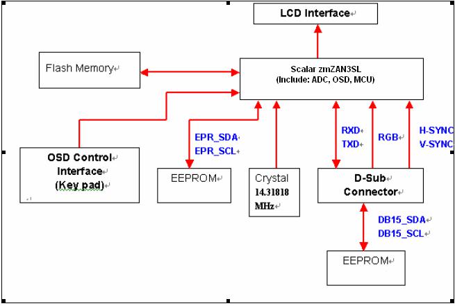
6.3 Electrical Block Diagram
6.3.1 Scalar Board Block Diagram
Page 16 of 69
HP L1902 Service Manual
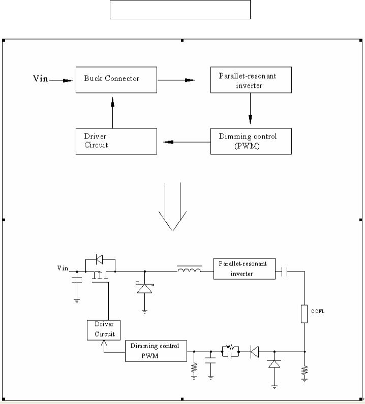
6.3.2 Inverter / Power Board Block Diagram
Inverter Block Diagram
Page 17 of 69

HP L1902 Service Manual
Power Block Diagram
Page 18 of 69

HP L1902 Service Manual
7.SCHEMATIC
7.1 SCALAR BOARD
7.1.1 For LG Panel +gmZAN3/SL Project
|
POWER BOARD |
|
REGULATOR -AIC3.3V |
|
|
|
|
|
|
|
|
|
|
|
|
|
|
|
|
|
|
|
|
||
AC-IN |
AC-IN |
+5.0V |
+5V |
+3.3V |
|
|
|
|
|
|
|
|
|
+5V |
+5V |
|
|
|
|
|
|
|
|
||
|
|
+12V |
REGULATOR -AIC1.8V |
|
|
|
|
|
|
|
|
|
|
+12V |
|
|
|
|
|
|
|
|
|
|
|
|
+5V |
+5V |
+3.3V |
|
|
|
|
|
|
|
|
|
|
|
|
|
|
|
|
|
|
|
|||
|
|
|
|
SCALER |
|
LVAVDD3.3 |
LVOUTVDD3.3 |
ADCAVDD333.3 |
RPLLAVDD3.3 |
ADCVDD1.8V |
RPLLVDD1.8V |
GMZAN3SL |
|
INPUT INTERFACE |
|
|
|
3.3 |
1.8VCVDD |
||||||
|
R |
|
|
RED+ |
RVDD |
|
|
|
|
|
|
|
|
G |
|
|
GREEN+ |
|
|
|
|
|
|
|
|
|
B |
|
|
BLUE+ |
|
|
|
|
|
|
|
LVDSO[0-9] |
|
|
|
|
|
|
|
|
|
|
|
||
|
|
|
HSI |
|
|
|
|
|
|
|
|
HSYNC |
|
|
|
|
|
LVDSE[0-9] |
|
|
|||
|
|
|
|
|
|
|
|
|
|
|
|
|
|
|
|
|
|
|
|
|
|||
|
|
|
VSI |
|
|
|
|
|
|
|
|
VSYNC |
|
|
|
|
|
|
|
|
GPIO0 |
|
BRIGHTNESS |
|
|
|
|
|
|
|
|
|
|
|
|
|
|
|
|
|
|
|
|
|
|||
|
|
DAT_DDC |
|
|
|
|
|
|
|
|
DDC-SDA |
|
|
|
|
|
|
|
GPIO7 |
|
LED_O |
||
|
|
|
|
|
|
|
|
|
|
|
|
|
|
|
|
|
|
|
|
|
|
||
|
|
CLK_DDC |
|
|
|
|
|
|
|
DDC-SCL |
|
|
|
|
|
|
|
|
|
||||
|
|
|
|
|
|
|
|
|
|
|
|
|
|
|
|
GPIO6 |
|
LED_G |
|||||
|
|
|
|
|
|
|
|
|
|
|
|
|
|
|
|
|
|
|
|
|
|
||
|
|
|
|
|
SDA |
SCL |
|
|
|
|
|
|
|
|
|
|
|
|
|
|
|
|
|
|
|
|
VGACON |
EDID-WP |
|
|
|
|
|
RESET_OUT |
|
|
|
|
|
|
PPWR |
|
PPWR |
||||
|
|
|
|
|
|
|
|
|
|
|
|
|
|
|
|
|
|
||||||
VSS |
TXD-DB |
RXD-DB |
VSS |
+5V |
EEPROM |
|
|
|
MEM_REG |
|
|
|
|
|
|
|
|
|
|
||||
|
|
|
|
|
|
|
M24LC02A |
|
|
|
HCLK/ALE |
|
|
|
|
|
|
|
PBIAS |
|
PBIAS |
||
|
|
|
|
|
|
|
|
|
|
|
|
|
|
|
|
|
|
|
|
|
|
||
|
|
|
|
|
|
|
|
|
|
|
|
|
|
|
|
|
|
|
|
|
|
|
|
|
|
|
|
|
|
|
|
|
|
|
GPIO13 |
GPIO12 |
GPIO11 |
HFS |
HDATA3 |
HDATA2 |
HDATA1 |
HDATA0 |
RDn |
WRn |
XTAL |
|
|
|
|
|
|
|
GND |
|
|
|
|
|
TCLK |
|
|
||||||||||
|
|
|
|
|
|
+5V |
|
|
|
|
|
|
|
|
|
|
|
|
|
|
VSS |
|
|
|
|
|
|
|
|
|
|
|
|
|
|
|
|
|
|
|
|
|
|
|
|
GND |
|
GND |
|
|
|
|
|
|
|
|
|
|
|
|
|
|
|
|
|
|
|
|
|
|
|
|
|
|
|
|
|
+5V |
|
|
|
|
|
|
|
|
|
|
|
|
|
|
|
|
|
|
|
|
|
|
|
|
|
|
|
|
|
|
|
|
|
|
|
|
|
|
|
|
|
|
|
|
|
|
GND |
|
VCC |
RST |
ALE |
P2.6 |
P0.7 |
P0.6 |
P0.5 |
P0.4 |
P0.3 |
P0.2 |
P0.1 |
P0.0 |
P3.7/RD# |
P3.6/WR# |
XTAL2 |
|
X2 |
|
|
|
|
|
|
P1.7/CEX4 |
|
|
|
|
|
|
|
|
|
|
|
|
|
|
|
||
|
|
|
|
|
|
|
|
|
|
|
|
|
|
|
|
|
|
|
|
|
|
||
|
|
|
|
|
|
|
VSS |
|
|
|
|
|
|
|
|
|
|
|
|
|
XTAL1 |
|
X1 |
|
|
|
|
|
|
|
P2.0 |
|
|
|
|
|
|
|
|
|
|
|
|
|
|
|
|
|
|
|
|
|
|
|
RXD |
|
|
|
|
P2.2 |
P2.3 |
P2.4 |
P2.5 |
|
|
|
P3.5 |
|
P3.4 |
/WP |
14.318MHZ |
|
|
|
|
|
|
|
TXD |
|
|
|
|
|
|
|
|
CRYSTAL |
|||||||
|
|
|
|
|
|
|
|
|
|
|
|
|
|
|
|
|
|
|
|
|
|
|
|
MICRO |
|
|
|
|
|
|
|
|
|
|
|
CONTROLLER |
KEYRIGHT |
|
ONOFFKEY |
|
|
|
|
|
|
|
|
|
MENUKEY |
KEYLEFT |
|
|
|
|
|
|
|||
|
|
|
SCL |
SDA |
|
WP |
|||||
|
W78E65P |
|
|
|
|
|
|
|
|
|
|
|
|
|
|
|
|
|
|
|
|
|
|
+5V 
 +5V
+5V
M24AC16
CON503
 LVDSO[0-9]
 LVDSE[0-9]
VLCD 
 VLCD
VLCD
GND
CON
GND
Title
MAIN BOARD BLOCK
Size |
Document Number |
715L1241-C |
|
|
Rev |
|
|
|
|
|
C |
||
Date: |
, 22, 2003 |
|
Sheet |
2 |
of 7 |
|
+3.3V_VDD |
|
|
|
|
|
|
|
|
|
|
3.3V_DVDD |
|
|
|
+1.8V_VDD |
|
|
|
|
|
|
|
|
|
|
|
|
|
|
|
|
|
|
|
|
|
|
|
|
|
|
|
|
|
|
|
|
|
|
|||
|
|
|
|
|
|
|
|
|
|
|
|
|
|
|
|
|
|
|
|
|
|
|
|
|
|
|
1.8V_DVDD |
|
|
|
|
|
|
|
|
|
|
|
|
|
|
|
|
|
|
|
|
|||||
|
|
|
58.27mA |
|
|
|
|
|
|
|
|
|
|
|
|
|
|
|
|
139mA |
|
|
|
|
|
|
|
|
|
|
|
|
|
|
|
|
|
|
|
|
|
|
|
|
|
|
|
|
||||
|
|
|
|
|
|
|
|
|
|
|
|
|
|
|
|
|
|
|
|
|
|
|
|
|
|
|
|
|
|
|
|
|
|
|
|
|
|
|
|
|
|
|
|
|
|
|
|
|
||||
|
|
L101 |
|
+ |
|
C123 |
C124 |
C125 |
C126 |
C127 |
C128 |
|
|
|
|
|
L102 |
+ |
|
C130 |
|
|
C131 |
C132 |
C133 |
|
C134 |
C135 |
|
|
|
|
|
|
|
|
|
|
|
|
|
|
|
|
|
|
|
|||||
|
120 OHM |
C122 |
|
0.1uF/16V |
0.1uF/16V |
0.1uF/16V 0.1uF/16V |
0.1uF/16V |
0.1uF/16V |
|
|
|
|
|
120 OHM |
C129 |
|
0.1uF/16V |
0.1uF/16V |
0.1uF/16V |
0.1uF/16V |
0.1uF/16V |
|
|
3.3V_DVDD |
|
|
1.8V_DVDD |
|
|
|
|
|
|
|||||||||||||||||||
|
|
22uF/16V |
|
|
|
|
|
|
|
|
22uF/16V |
|
0.1uF/16V |
|
|
|
|
|
|
|
|
|
|
|||||||||||||||||||||||||||||
|
|
|
GND |
|
|
Close to respective power Pins |
|
|
|
|
|
|
|
|
|
GND |
|
|
|
Close to respective power Pins |
|
|
|
|
|
|
|
|
|
|
|
|
|
|
|
|
|
|
|
|
|
|||||||||||
|
|
|
|
|
|
|
|
|
|
|
|
|
|
|
|
|
|
|
|
|
|
|
|
|
|
|
|
|
|
|
U102 |
|
|
|
|
|
|
|
|
|
|
|
|
|
|
|
|
|
||||
|
|
|
|
|
|
|
|
3.3V_AVDD |
|
|
|
|
|
|
|
|
|
|
|
|
|
1.8V_AVDD |
|
|
|
|
|
3.3V_PVDD |
|
|
|
|
|
|
|
|
|
|
|
|
|
|
|
3.3V_LAVDD |
|
|
|
|||||
|
|
|
83.4mA |
|
|
|
|
|
|
|
|
|
|
|
|
|
|
|
|
42.2mA |
|
|
|
|
|
3.3V_AVDD |
|
|
33 51 94 |
|
|
31 47 65 67 92 99 |
|
|
|
|
|
|||||||||||||||
|
|
L103 |
|
C137 |
C138 |
|
|
|
|
|
|
|
|
|
|
L104 |
C141 |
|
C142 |
|
|
|
|
|
|
|
|
|
|
|
|
|
|
|
|
|||||||||||||||||
|
|
|
|
|
|
|
|
|
|
|
|
|
|
|
|
|
|
|
|
|
|
|
|
|
|
|
3.3 |
3.3 |
3.3 |
|
|
1.8 |
1.8 |
1.8 |
1.8 |
1.8 |
1.8 |
|
|
3.3V_DVDD |
|
|
||||||||||
|
|
22uF/16V |
+ |
|
|
|
|
|
|
3.3V_PVDD |
|
|
|
|
|
|
|
|
22uF/16V |
+ |
|
|
|
|
|
|
|
|
|
|
|
69 |
|
RVDD |
RVDD |
RVDD |
|
|
CVDD |
CVDD |
CVDD |
CVDD |
CVDD |
CVDD |
AVDD_LV_3.3 |
|
|
|
|
|
||
|
120 OHM |
C136 |
|
0.1uF/16V |
0.1uF/16V |
Close to respective power Pins |
|
|
|
|
|
120 OHM |
C140 |
0.1uF/16V |
0.1uF/16V |
|
|
|
|
|
|
|
|
|
|
|
|
|
|
|
|
|
|
|
|
|
1 |
|
|
|
|
|||||||||||
|
|
|
|
|
|
|
|
|
|
|
|
|
|
|
|
|
|
|
|
|
|
|
|
|
|
|
|
|
|
|
|
|
|
|
|
|
|
|
|
|
|
|
|
|
||||||||
|
|
|
|
|
|
|
|
|
|
|
|
|
|
|
|
|
|
|
|
|
|
|
|
|
|
|
|
|
|
|
|
|
|
79 |
AVDD_ADC_3.3 |
|
|
|
|
|
|
|
|
|
|
|
|
4 |
|
|
|
|
|
|
|
|
|
|
|
|
|
|
|
|
|
|
|
|
|
|
|
|
|
|
|
|
|
|
|
|
|
|
|
|
1.8V_AVDD |
89 |
AVDD_ADC_3.3 |
|
|
|
|
|
|
|
|
|
|
|
VDD_OUT_LV_3.3 |
16 |
|
|
|
|
|
|
|
|
GND |
|
|
|
|
|
|
|
|
|
|
|
|
|
|
|
|
GND |
|
|
|
|
|
|
|
|
|
|
|
|
AVDD_RPLL_3.3 |
|
|
|
|
|
|
|
|
|
|
|
VDD_OUT_LV_3.3 |
28 |
|
|
|
|
||
|
|
|
|
|
|
|
|
|
8.1mA |
|
|
|
|
|
|
|
|
|
|
|
|
|
|
|
|
|
|
|
|
|
84 |
VDD_RPLL_1.8 |
|
|
|
|
|
|
|
|
|
|
|
VDD_OUT_LV_3.3 |
|
|
|
|
|
|||
|
|
|
|
|
|
|
|
|
|
|
|
|
|
|
|
|
|
|
|
|
|
|
|
|
|
|
|
|
|
|
|
|
|
82 |
|
|
|
|
|
|
|
|
|
|
|
|
|
|
|
|
|
|
|
|
|
|
|
|
|
|
|
|
|
|
|
|
|
|
|
|
|
|
|
|
|
|
|
|
|
|
|
|
|
|
|
|
|
VDD_ADC_1.8 |
|
|
|
|
|
|
|
|
|
|
|
|
|
|
|
|
|
|
|
|
|
3.3V_LAVDD |
|
|
L106 |
C139 |
|
|
|
|
|
|
|
|
|
|
|
|
|
|
|
|
|
|
|
|
|
|
|
|
|
|
|
|
|
|
|
|
|
|
AVSS_LV |
3 |
|
|
|
|
||||
|
|
|
|
|
|
|
|
|
120 OHM |
|
|
|
|
|
|
|
|
|
|
|
|
|
|
|
|
|
|
|
|
|
|
|
81 |
GND_ADC |
|
|
|
|
|
|
|
|
|
|
|
15 |
|
|
|
|
||
|
|
|
6.4mA |
|
|
|
|
|
|
|
0.1uF/16V |
|
|
|
|
|
|
|
|
|
|
|
|
|
|
|
|
|
|
|
|
|
|
|
|
|
|
|
|
|
|
|
|
|
VSS_OUT_LV |
27 |
|
|
|
|
||
|
|
|
|
|
|
|
|
|
|
|
|
|
|
|
|
|
|
|
|
|
|
|
|
|
|
|
|
|
|
|
72 |
|
|
|
|
|
|
|
|
|
|
|
|
VSS_OUT_LV |
|
|
|
|
||||
|
|
|
|
|
|
|
|
|
|
|
|
|
|
|
|
|
|
|
|
|
|
|
|
|
|
|
|
|
|
|
|
|
|
76 |
AGND_ADC |
|
|
|
|
|
|
|
|
|
|
|
|
|
GND |
|
|
|
|
|
L105 |
|
|
|
|
|
|
|
|
|
|
|
|
|
|
|
|
|
|
|
|
|
|
|
|
|
|
|
|
|
|
|
80 |
AGND_ADC |
|
|
|
|
|
|
|
|
|
|
|
|
|
|
|
|
|
|
120 OHM |
+ C143 |
C144 |
|
|
|
|
|
|
|
|
|
|
|
|
|
|
|
|
|
|
|
|
|
|
|
|
|
|
|
|
AGND_ADC |
|
|
|
|
|
|
|
|
|
|
|
CH3P_LV_E/R0 |
5 |
LVDS_E9 |
|
|
|
|||
|
|
|
|
|
|
|
|
|
|
|
|
|
|
|
|
|
|
|
|
|
|
|
|
|
|
|
|
|
|
|
|
|
|
83 |
|
|
|
|
|
|
|
|
|
|
|
|
6 |
LVDS_E8 |
|
|
|
|
|
|
10uF |
|
0.1uF/16V |
|
|
|
|
|
|
|
|
|
|
|
|
|
|
|
|
|
|
|
|
|
|
|
|
|
|
86 |
VSS_RPLL |
|
|
|
|
|
|
|
|
|
|
|
CH3N_LV_E/R1 |
7 |
LVDS_E7 |
|
|
|
|||
GND |
|
|
|
|
|
|
|
|
|
|
|
|
|
|
|
|
|
|
|
|
|
|
|
|
|
|
|
|
|
|
|
|
|
|
AVSS_RPLL |
|
|
|
|
|
|
|
|
|
|
|
CLKP_LV_E/R2 |
8 |
LVDS_E6 |
|
|
|
|
|
|
|
|
|
|
|
|
|
|
GND |
|
|
|
|
|
|
|
|
|
|
|
|
|
|
|
|
|
|
|
|
|
|
|
|
|
|
|
|
|
|
|
|
|
|
|
CLKN_LV_E/R3 |
9 |
LVDS_E5 |
|
|
|
|
|
|
|
|
|
|
|
|
|
|
|
|
|
|
|
|
|
|
|
|
|
|
|
|
|
|
|
|
|
|
|
|
|
|
|
|
|
|
|
|
|
|
|
|
|
CH2P_LV_E/R4 |
|
|
|
|||
|
|
|
|
|
|
|
|
|
|
|
|
|
|
|
|
|
|
|
|
|
|
|
|
|
|
|
|
|
|
|
|
|
|
|
|
|
|
|
|
|
|
|
|
|
|
|
10 |
LVDS_E4 |
|
|
|
|
|
|
|
|
|
|
|
|
|
|
|
|
|
|
|
|
|
|
|
|
|
|
|
|
|
|
|
|
|
|
|
C176 |
NC |
GND |
|
|
|
|
|
|
|
|
|
|
|
|
|
CH2N_LV_E/R5 |
11 |
LVDS_E3 |
|
|
|
GND |
|
|
|
GND |
|
|
|
|
|
|
|
|
|
|
|
|
|
|
|
|
|
|
|
|
|
|
|
3.3V_PVDD |
|
|
|
|
|
|
|
|
|
|
|
|
|
|
|
|
CH1P_LV_E/R6 |
12 |
LVDS_E2 |
|
|
|
||
|
|
|
|
|
|
|
|
|
|
|
|
|
|
|
|
|
|
|
|
|
|
|
|
|
|
|
|
|
|
|
87 |
|
|
|
|
|
|
|
|
|
|
|
|
CH1N_LV_E/R7 |
13 |
LVDS_E1 |
|
|
|
|||
|
|
|
|
|
|
|
|
|
|
|
|
|
|
|
|
|
|
|
|
|
|
|
R121 22 1/16W |
|
|
|
|
|
|
|
|
|
|
|
|
|
|
|
|
|
|
|
|
CH0P_LV_E/G0 |
14 |
LVDS_E0 |
|
|
|
|||
|
|
|
|
|
|
|
|
|
|
|
|
|
|
|
|
|
|
|
|
|
|
|
|
|
|
|
|
|
|
X102 |
88 |
XTAL |
|
|
|
|
|
|
|
|
|
|
|
CH0N_LV_E/G1 |
|
|
LVDS_E[0..9] |
|
|
|||
|
|
|
|
|
|
|
|
|
|
|
|
|
|
|
|
|
|
|
|
|
|
|
|
|
|
|
|
|
|
|
|
|
NC |
TCLK |
|
|
|
|
|
|
|
|
|
|
|
|
|
|
LVDS_E[0..9] |
4 |
||
|
|
|
|
|
|
|
|
|
|
|
|
|
|
|
|
|
|
|
|
|
|
|
|
|
|
|
|
|
3.3V_PVDD |
|
|
|
|
|
|
|
|
|
|
|
|
|
|
|
|
|
|
|||||
|
|
|
|
|
|
|
|
|
|
|
|
|
|
|
|
|
|
|
|
|
|
|
|
|
|
|
|
|
|
|
|
|
|
|
|
|
|
|
|
|
|
|
|
|
CH3P_LV_O/G2 |
17 |
LVDS_O9 |
|
|
|
||
|
|
|
|
|
|
|
|
|
|
|
|
|
|
|
|
|
|
|
|
|
|
|
|
|
|
|
|
|
|
|
|
|
|
|
|
|
|
|
|
|
|
|
|
|
|
|
18 |
LVDS_O8 |
|
|
|
|
|
|
|
|
|
|
|
|
|
|
|
|
|
|
|
|
|
|
|
|
|
|
|
|
|
|
|
|
|
|
|
C177 NC |
|
|
|
|
|
|
|
|
|
|
|
|
|
|
CH3N_LV_O/G3 |
19 |
LVDS_O7 |
|
|
|
|
|
|
|
|
|
|
|
|
|
|
|
|
|
|
|
|
|
|
|
|
|
|
|
|
|
|
|
|
|
|
|
|
|
|
|
|
|
|
|
|
|
|
|
|
|
|
|
CLKP_LV_O/G4 |
20 |
LVDS_O6 |
|
|
|
|
|
|
|
|
|
|
|
|
|
|
|
|
|
|
|
|
|
|
|
|
|
|
|
|
|
|
|
|
|
|
|
|
|
|
|
|
|
|
|
|
|
|
|
|
|
|
CLKN_LV_O/G5 |
21 |
LVDS_O5 |
|
|
|
|
|
|
|
|
|
|
|
|
|
|
|
|
|
|
|
|
|
|
|
|
|
|
|
|
|
|
|
|
|
|
|
|
|
|
|
|
|
|
|
|
|
|
|
|
|
|
CH2P_LV_O/G6 |
22 |
LVDS_O4 |
|
|
|
|
|
|
|
|
|
|
|
|
|
|
|
|
|
|
|
|
|
|
|
|
|
|
1 |
RED+ |
|
|
|
|
|
|
|
|
77 |
RED+ |
|
|
|
|
|
|
|
|
|
|
|
CH2N_LV_O/G7 |
23 |
LVDS_O3 |
|
|
|
|
|
|
|
|
|
|
|
|
|
|
|
|
|
|
|
|
|
|
|
|
|
|
|
|
|
|
|
|
|
|
|
78 |
|
|
|
|
|
|
|
|
|
|
|
CH1P_LV_O/B0 |
24 |
LVDS_O2 |
|
|
|
||||
|
|
|
|
|
|
|
|
|
|
|
|
|
|
|
|
|
|
|
|
|
|
|
1 |
RED- |
|
|
|
|
|
|
|
|
74 |
RED- |
|
|
|
|
|
|
|
|
|
|
|
CH1N_LV_O/B1 |
25 |
LVDS_O1 |
|
|
|
|
|
|
|
|
|
|
|
|
|
|
|
|
|
|
|
|
|
|
|
|
|
|
|
1 |
GREEN+ |
|
|
|
|
|
|
|
75 |
GREEN+ |
|
|
|
|
|
|
|
|
|
|
|
CH0P_LV_O/B2 |
26 |
LVDS_O0 |
|
|
|
||
|
|
|
|
|
|
|
|
|
|
|
|
|
|
|
12/22 |
|
|
|
|
|
|
|
1 |
GREEN- |
|
|
|
|
|
|
|
70 |
GREEN- |
|
|
|
|
|
|
|
|
|
|
|
CH0N_LV_O/B3 |
|
|
|
|
|
||
|
|
|
|
|
|
|
|
|
|
|
|
|
|
|
|
|
|
|
+5V +5V |
|
1 |
BLUE+ |
|
|
|
|
|
|
|
|
71 |
BLUE+ |
|
|
|
|
|
|
|
|
|
|
|
|
|
|
LVDS_O[0..9] |
LVDS_O[0..9] |
4 |
|||
|
|
|
|
|
|
|
|
|
|
|
|
|
|
|
CHANGE NVRAM_SCL |
|
|
|
|
|
1 |
BLUE- |
|
|
|
|
|
|
|
|
|
BLUE- |
|
|
|
|
|
|
|
|
|
|
|
|
|
|
|
|||||
|
|
|
|
|
|
|
|
|
|
|
|
|
|
|
P3.5/T1 => P1.4/CEX1 |
|
|
|
|
|
1 |
HSYNC |
|
|
|
|
|
|
|
|
95 |
HSYNC |
|
|
|
|
|
|
|
|
|
|
|
PPWR |
30 |
PPWR |
PPWR |
5 |
|
|||
|
|
|
|
|
|
|
|
|
|
|
|
|
|
|
|
|
|
|
|
|
|
|
|
|
|
|
|
96 |
|
|
|
|
|
|
|
|
|
|
|
29 |
PBIAS |
|
||||||||||
|
|
|
|
|
|
|
|
|
|
|
|
|
|
|
CHANGE NVRAM_SDA |
|
|
|
|
|
1 |
VSYNC |
|
|
|
|
|
|
|
|
73 |
VSYNC |
|
|
|
|
|
|
|
|
|
|
|
PBIAS |
|
|
PBIAS |
5 |
|
|||
|
|
|
|
|
|
|
|
|
|
|
|
|
|
|
|
R122 |
|
R123 |
|
|
|
|
|
|
|
|
|
|
|
|
SOG_MCSS |
|
|
|
|
|
|
|
|
|
|
|
|
|
|
|
|
|
||||
|
|
|
|
|
|
|
|
|
|
|
|
|
|
|
P3.4/T0 => P1.3/CEX0 |
|
|
|
|
|
|
|
|
|
|
|
|
|
|
|
|
|
|
|
|
|
|
|
|
|
|
|
|
|
|
|
|
|||||
|
|
|
|
|
|
|
|
|
|
|
|
|
|
|
4.7K 1/16W |
|
4.7K 1/16W |
|
|
|
|
|
|
|
|
|
|
|
|
|
|
|
|
|
|
|
|
|
|
|
|
|
|
|
|
|
|
|||||
|
|
|
|
|
|
|
|
|
|
|
|
|
|
|
|
|
|
|
|
|
|
|
|
|
|
|
|
|
|
|
|
|
|
|
|
|
|
|
|
|
|
|
|
|
|
|
|
|
||||
|
|
|
|
|
|
|
|
|
|
|
|
|
R124-RESET |
RESET |
|
|
|
|
|
|
|
|
|
|
|
|
|
|
|
|
91 |
|
|
|
|
|
|
|
|
|
|
|
|
NC |
49 |
|
|
|
|
|||
|
|
|
|
|
|
|
|
|
|
|
|
|
FUNCTION |
|
|
|
|
|
|
|
|
|
|
|
|
|
|
|
|
|
RESET_OUT |
|
|
|
|
|
|
|
|
|
|
|
61 |
|
|
|
|
|||||
|
|
|
|
|
|
|
|
|
|
|
|
|
|
|
|
|
|
|
|
|
|
|
|
|
|
|
|
|
|
|
|
|
|
|
|
|
|
|
|
|
|
|
NC |
66 |
|
|
|
|
||||
|
|
|
|
|
|
|
|
|
|
|
|
|
|
|
R124 |
NC |
|
|
|
|
|
|
|
|
|
|
|
|
|
|
|
|
|
90 |
|
|
|
|
|
|
|
|
|
|
|
|
NC |
|
|
|
|
|
|
|
|
|
|
|
|
|
|
|
|
|
|
|
|
|
|
|
|
|
|
|
|
|
|
|
|
|
|
|
|
|
|
C145 |
RESETn |
|
|
|
|
|
|
|
|
|
|
|
|
|
|
|
|
|
|
|
|
|
|
|
|
|
|
|
|
|
|
|
|
|
|
R126 |
|
|
|
U101 |
|
|
|
|
|
|
|
|
|
|
|
|
|
|
|
|
|
|
|
|
|
|
|
|
52 |
|
|
|
|
|||
ONLY |
|
|
+5V |
|
|
R129 |
|
|
|
|
|
|
1/16W4.7K |
R175 |
|
|
9 |
|
A14/P2.6 |
31 |
|
A15 |
|
|
|
1 |
DDC_SCL |
DDC_SDA |
98 |
DDC_SCL |
|
|
|
|
|
|
|
|
|
|
|
|
|
|
|
|
||||||
|
|
|
|
|
|
|
|
|
GND |
1001/16W |
|
|
P1.6/CEX3/WAIT# |
|
|
|
|
|
|
|
|
|
|
|
|
|
|
|
GPIO0/PWM0 |
53 |
|
BRIGHTNESS |
5 |
|
||||||||||||||||||
|
|
|
|
|
|
|
|
|
|
|
|
|
+5V |
|
|
|
|
|
|
|
|
|
|
|
|
|
|
|
|
|
0.1uF/16V |
|
|
|
|
|
|
|
|
|
|
|
|
|
|
|
||||||
|
|
|
|
|
|
|
|
|
|
|
|
|
|
|
|
|
SP1 |
|
2 |
P1.0/T2 |
|
A8/P2.0 |
24 |
|
R125 |
|
VGA_CAB |
|
VGA_CAB 1 |
|
|
|
|
|
|
|
|
|
|
|
|
|
|
GPIO1/PWM1 |
|
|
|
|
|
|||
OPTIONAL |
|
|
|
+5V |
|
|
|
|
12/22 BOM/LAYOUT Add |
|
|
|
SP2 |
|
3 |
P1.1/T2EX |
|
A9/P2.1 |
25 |
KEY_MENU |
|
100 1/16W |
|
|
|
GND |
|
|
|
|
|
|
|
|
|
|
|
|
|
|
54 |
|
|
|
|
|||||||
FOR |
|
|
|
|
|
|
|
|
|
R174,R175 |
|
|
|
|
|
NVRAM_SDA |
5 |
P1.2/ECI |
|
A10/P2.2 |
27 |
KEY_RIGHT |
|
|
|
|
|
IRQn |
46 |
|
|
|
|
|
|
|
|
|
|
|
|
GPIO2/DHS |
55 |
|
|
|
|
|||||
DEBUGGING |
|
|
|
|
|
|
|
|
|
|
R174 |
|
|
|
NVRAM_SCL |
6 |
P1.3/CEX0 |
|
A11/P2.3 |
28 |
KEY_LEFT |
|
|
R127 |
|
|
|
|
GPIO10/IRQn |
|
|
|
|
|
|
|
|
|
|
|
GPIO3/DVS |
56 |
|
|
|
|
||||||
PURPOSES |
|
|
|
|
|
|
|
|
|
|
100 1/16W |
|
|
|
/WP |
|
7 |
P1.4/CEX1 |
|
A12/P2.4 |
29 |
KEY_ONOFF |
|
|
|
|
|
|
|
|
|
|
|
|
|
|
|
|
|
|
|
GPIO4/DEN |
57 |
|
|
|
|
|||||
|
|
|
|
|
|
|
|
|
|
|
|
|
|
|
AUDIO_STDBY |
8 |
P1.5/CEX2 |
|
A13/P2.5 |
30 |
|
A14 |
|
|
4.7K 1/16W |
|
DDC_SCL |
97 |
|
|
|
|
|
|
|
|
|
|
|
|
GPIO5/DCLK |
|
|
|
|
|
||||||
|
|
|
|
R128 |
|
|
.4 |
|
|
1 |
EDID-WP |
|
|
|
|
|
|
|
10 |
P1.7/CEX4/A17/W |
A15/P2.7 |
32 |
|
|
SP6 |
|
|
1 |
DDC_SDA |
|
|
DDC_SDA |
|
|
|
|
|
|
|
|
|
|
|
|
58 |
|
|
|
|
|||
|
|
|
|
7K.4 |
|
|
7K |
|
|
|
|
|
|
|
|
UDART_DI |
|
|
RST |
|
|
PSEN# |
|
|
|
|
|
|
|
|
|
|
|
|
|
|
|
|
|
|
|
|
|
|
|
GPIO6/B7 |
|
LED_O |
3 |
|
||
|
|
|
|
|
|
|
|
|
|
|
1 |
|
RXD |
|
11 |
P3.0/RXD |
|
AD7/P0.7 |
36 |
|
|
|
|
+5V |
|
|
|
|
38 |
GPIO13/AD7 |
|
|
|
|
|
|
|
|
|
|
|
59 |
|
|
||||||||
|
CN102 |
|
|
|
|
|
|
|
|
|
UDART_DO |
|
13 |
|
37 |
|
|
|
|
|
|
|
|
|
39 |
|
|
|
|
|
|
|
|
|
|
|
GPIO7/B4 |
60 |
|
LED_G |
3 |
|
||||||||||
C146 |
|
1/16W |
|
|
UDART_DI |
|
|
|
|
1 |
|
TXD |
|
|
|
14 |
P3.1/TXD |
|
AD6/P0.6 |
38 |
|
|
|
|
|
|
|
|
|
40 |
GPIO12/AD6 |
|
|
|
|
|
|
|
|
|
|
|
GPIO8/B6 |
50 |
|
|
|
|
||||
|
2 |
|
|
|
|
|
|
TCLK |
|
|
|
|
|
17 |
P3.4/T0 |
|
AD3/P0.3 |
41 |
|
|
|
|
|
|
|
|
|
43 |
HDATA3/AD3 |
|
|
|
|
|
|
|
|
|
|
|
GPIO9/B5 |
|
|
|
|
|
||||||
|
|
1 |
|
|
|
|
UDART1/16W_DO |
|
|
|
|
|
|
|
|
|
|
15 |
P3.2/INT0# |
|
AD5/P0.5 |
39 |
|
|
|
|
|
|
|
|
|
41 |
GPIO11/AD5 |
|
|
|
|
|
|
|
|
|
|
|
|
|
|
|
|
|||
|
|
|
|
|
|
|
|
|
|
|
|
|
|
|
16 |
P3.3/INT1# |
|
AD4/P0.4 |
40 |
|
|
|
|
|
|
|
|
|
42 |
HFS/AD4 |
|
|
|
|
|
|
|
|
|
|
|
|
|
|
|
|
|
|||||
|
|
3 |
|
|
|
|
|
|
|
|
|
|
|
X101 |
|
|
|
|
P3.5/T1 |
|
AD2/P0.2 |
42 |
|
|
|
|
|
|
|
|
|
44 |
HDATA2/AD2 |
|
|
|
|
|
|
|
|
|
|
|
|
|
|
|
|
|
||
0.1uF/16V |
|
4 |
|
|
|
|
|
|
|
|
TCLK FOR ZAN3SL |
14.318MHz |
|
|
|
|
|
|
AD1/P0.1 |
43 |
|
|
|
function |
|
|
|
|
|
45 |
HDATA1/AD1 |
|
|
|
|
|
|
|
|
|
|
|
|
|
|
|
|
|
||||
|
|
|
|
|
|
|
|
|
|
|
|
20 |
|
|
|
AD0/P0.0 |
|
|
|
|
|
|
|
|
HDATA0/AD0 |
|
|
|
|
|
|
|
|
|
|
|
|
|
|
|
|
|
||||||||||
|
|
|
|
|
|
|
|
|
|
|
|
|
|
|
|
|
|
|
21 |
XTAL2 |
|
ALE/PROG# |
18 |
|
WRn |
|
|
|
|
|
|
|
|
|
|
|
|
|
|
|
|
|
|
|
|
|
|
|
|
|
||
|
|
|
|
|
|
|
|
|
|
|
|
|
|
|
|
|
|
|
|
XTAL1 |
|
P3.6/WR# |
19 |
|
RDn |
|
|
|
|
|
|
|
|
|
|
|
|
|
|
|
|
|
|
|
|
|
|
|
|
|
|
|
|
G-PROBE |
|
|
|
|
|
|
|
|
|
|
|
|
|
|
+5V |
|
35 |
|
|
|
P3.7/RD#/A16 |
33 |
|
ALE |
|
|
R173 |
|
|
|
|
|
|
|
|
|
|
|
|
|
|
|
|
|
|
|
|
|
|
||
|
GND |
|
|
|
|
|
|
|
|
|
|
|
|
|
|
|
EA#/VPP |
|
|
|
|
|
R130 |
ISP |
|
|
|
|
|
|
|
|
|
|
|
|
|
|
|
|
|
|
|
|
|
|
||||||
|
|
|
|
|
|
|
|
|
|
|
|
|
|
|
|
|
|
44 |
|
|
|
|
|
NC |
|
|
|
|
|
|
|
|
|
|
|
|
|
|
|
|
|
|
|
|
|
|
|
|||||
|
|
|
|
|
|
|
|
|
|
|
|
|
C147 |
|
|
C148 |
|
|
|
VCC |
|
|
NC |
34 |
|
SP7 |
|
|
|
|
|
|
|
|
|
|
|
|
|
|
|
|
|
|
|
|
|
|
|
|
|
|
|
|
|
|
|
|
|
|
|
|
|
|
|
10pF |
|
|
10pF |
C149 |
|
W78E65P |
|
23 |
|
SP8 |
NC |
Hardwave |
|
|
|
|
|
|
|
|
|
|
|
|
|
|
|
|
|
|
|
|
|
|
|
|
|||
|
|
|
|
|
|
|
|
|
|
|
|
|
|
|
|
|
|
|
|
NC |
12 |
|
|
|
|
|
|
|
|
|
|
|
|
|
|
|
|
|
|
|
|
|
|
|
|
|
|
|||||
|
|
|
|
+5V |
|
|
|
|
|
|
|
|
|
|
|
0.1uF/16V |
|
22 |
VSS |
|
|
NC |
1 |
|
|
|
|
|
|
|
|
|
|
|
|
|
|
|
|
|
|
|
|
|
|
VBUFS_RPLL |
85 |
SP10 |
GND |
|
|
|
|
|
|
|
|
|
|
|
|
|
|
|
|
GND |
|
|
GND |
|
|
|
|
|
NC |
|
|
|
|
|
|
|
|
|
|
|
|
|
|
|
|
|
|
|
|
|
|
|
2 |
SP11 |
GND |
|
|
||
|
|
C150 |
|
R133 |
R134 R135 |
|
|
|
|
|
|
|
|
|
|
|
|
|
|
|
|
|
|
|
|
+5V |
|
|
|
|
|
|
|
|
|
|
|
|
|
|
|
|
|
VCO_LV |
|
|
|
|
|
|||
|
|
0.1uF/16V |
.4 |
.4 |
.4 |
12/22 BOM R135 NC CHANGE TO 4.7K OHM |
|
|
|
GND |
|
PLCC44 - SOCKET-87L202-44 |
|
|
+ C107 |
|
|
|
RDn |
|
|
37 |
RDn |
|
|
|
|
|
|
|
|
|
|
|
|
62 |
|
GND |
|
|
||||||||||||
|
|
|
|
|
|
|
|
|
|
|
|
|
|
|
|
|
|
|
|
|
|
|
|
|
|
WRn |
|
|
36 |
|
|
|
|
|
|
|
|
|
|
|
STI_TM1 |
|
|
|
|
|||||||
|
|
|
|
7K |
7K |
7K |
|
|
|
|
|
|
|
|
|
|
|
Philips P89C51RD2 |
|
+5V |
|
NC |
|
|
|
|
|
|
|
|
35 |
WRn |
|
|
|
|
|
|
|
|
|
|
|
63 |
|
|
|
|
||||
|
|
|
|
|
|
|
|
|
|
|
|
|
|
|
Winbond W77E65P-24/40 |
|
|
|
|
|
|
|
|
|
|
|
34 |
HCLK/ALE |
|
|
|
|
|
|
|
|
|
|
|
STI_TM2 |
|
|
|
|
|
|||||||
|
IC104 |
|
|
|
|
|
|
12/22 BOM R137 NC CHANGE TO 100 OHM |
|
|
|
|
GND |
|
|
|
|
|
|
|
|
MEM_REG |
|
|
|
|
|
|
|
|
|
|
|
|
|
|
|
|
|
|||||||||||||
1 |
A0 |
VCC |
8 |
1/16W |
1/16W |
1/16W |
|
|
|
/WP |
|
|
|
|
|
|
|
SyncMOS SM2965 |
|
|
R138 |
NC |
|
|
|
A15 |
R136 |
NC |
|
|
|
|
CRVSS |
CRVSS CRVSS CRVSS CRVSS CRVSS |
|
|
|
|
|
|
|
|
|
|
|
|||||||
2 |
7 |
|
|
|
R137 |
100 1/16W |
|
|
|
|
|
|
WINBOND W78E65P-40-56L1125-137-X |
|
|
|
|
|
|
|
|
|
|
|
|
|
|
|
|
|
|
|
|
|
|
|
|
|
GND |
|
|
|
||||||||||
3 |
A1 |
WP |
6 |
|
|
|
R139 |
100 1/16W |
NVRAM_SCL |
|
|
|
|
|
|
|
|
|
|
|
|
|
|
|
|
|
|
|
|
|
|
|
|
|
|
|
|
|
|
|
|
|
|
|
|
|
|
|
|
|||
4 |
A2 |
SCK |
5 |
|
|
|
R141 |
100 1/16W |
NVRAM_SDA |
|
|
|
|
|
|
|
|
|
|
|
|
|
|
|
|
|
|
|
|
R142 |
0 1/16W |
|
|
|
|
|
|
|
|
|
|
|
|
|
|
|
|
|
|
|
||
|
VSS |
SI |
|
|
|
|
|
|
|
|
|
|
|
|
|
|
|
|
|
|
|
|
|
R140 |
NC |
|
|
|
ALE |
|
|
|
|
|
|
|
|
|
|
|
|
|
|
|
|
|
|
|
|
|
||
GND |
M24C16-MN6T |
R145 |
1/16W15K |
|
|
|
|
|
|
|
|
|
|
|
|
|
|
|
|
|
12/22 Add C107 PCB |
R14310K |
|
R14410K |
A14 |
R146 |
0 1/16W |
|
|
|
|
|
|
|
100 |
|
|
|
|
|
|
|
|
|
|
|
||||||
|
|
|
|
12/22 BOM R145 10K CHANGE TO 15K OHM |
|
|
|
|
|
|
|
|
|
|
LOCATION 10UF |
|
|
|
|
PQFP-100 |
|
32 48 |
64 68 |
93 |
|
|
|
|
|
|
|
|
|
|
|
|||||||||||||||||
|
|
|
|
|
|
|
|
|
|
|
|
|
|
|
|
|
|
|
|
|
|
|
|
|
|
|
|
|
|
|
Refer BOOTSTRAP OPTIONS |
|
GMZAN3/SL |
|
|
|
|
|
|
|
|
|
|
|
|
|
|
|
|
|
||
|
|
|
|
GND |
|
|
|
|
|
|
|
|
|
|
|
|
|
|
|
|
|
|
|
|
|
|
|
|
|
|
|
|
|
|
|
|
|
|
GND |
|
|
|
|
|
|
|
|
|
|
|
|
|
|
|
|
|
|
|
|
|
|
|
|
|
|
|
|
|
|
|
|
|
|
|
|
|
|
|
|
|
GND |
|
|
|
|
|
|
|
|
|
|
|
|
|
|
|
|
|
|
|
|
|
|
|
|
3 KEY_MENU
3 KEY_RIGHT
3 KEY_LEFT
3 KEY_ONOFF
3 AUDIO_STDBY
|
|
|
|
|
|
+5V |
|
|
|
4.7K 1/16W |
|
||||||
KEY_MENU |
1 |
RP103 |
8 |
|
|
KEY_UP => A9/P2.1 OF MCU |
||
|
|
|
||||||
KEY_RIGHT |
2 |
|
7 |
|
|
KEY_RIGHT => A10/P2.2 OF MCU |
||
KEY_LEFT |
3 |
|
6 |
|
|
KEY_DOWN => A11/P2.3 OF MCU |
||
KEY_ONOFF |
4 |
|
5 |
|
|
KEY_LEFT => A12/P2.4 OF MCU |
||
A14 |
R147 |
4.7K 1/16W |
|
KEY_ON/OFF => A13/P2.5 OF MCU |
||||
|
|
|
|
|
|
|
A14 => MEM_REG(ZAN3SL) |
|
A15 |
R148 |
4.7K 1/16W |
|
|||||
|
|
|
|
|
|
|
A15 => HCLK(ZAN3SL) |
|
AUDIO_STDBY |
R149 |
4.7K 1/16W |
|
|||||
|
|
|
|
|
|
|
|
|
Title
ZAN3SL & Micro I/F
Size |
Document Number |
|
|
|
Rev |
C |
715L1241-C |
|
|
|
C |
Date: |
, 22, 2003 |
Sheet |
4 |
of 7 |
|
Page 19 of 69
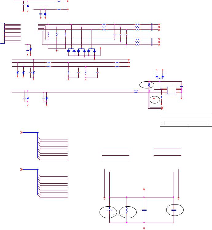
|
DB-RXD |
|
|
|
|
|
R102 |
|
|
|
C102 |
|
D102 |
|
|
|
|
|
|
56pF |
|
MLL5232B |
|
|
|
|
|
|
|
|
DB-TXD |
|
|
R103 |
|
|
|
GND |
GND |
6V.5 |
C103 |
D103 |
|
|
|
|
|
|
MLL5232B |
|
|||
|
|
|
|
56pF |
|
|
||
|
|
|
|
|
GND |
GND |
6V.5 |
|
CN301 |
PC5V |
|
|
|
R |
|
|
|
1 |
HSI |
|
|
|
|
|
||
|
|
|
gndR |
|
|
|
||
2 |
|
VSI |
|
|
G |
|
|
|
3 |
CLK_DDC |
|
|
|
gndG |
|
|
|
4 |
DAT_DDC |
|
|
|
B |
|
|
|
5 |
DB-TXD |
|
|
|
gndB |
|
1/16W |
R107 1/16W |
6 |
DB-RXD |
|
|
|
|
R106 |
||
9 |
|
|
|
|
||||
7 |
VGA_CON |
|
|
|
|
|
|
|
8 |
B |
|
|
|
|
|
|
|
|
gndB |
|
|
|
|
|
|
|
10 |
|
|
|
|
|
75 |
75 |
|
G |
|
|
|
|
||||
11 |
|
gndG |
|
|
|
|
|
|
12 |
|
|
|
|
|
|
|
|
R |
|
|
|
|
|
|
||
13 |
|
gndR |
|
|
|
|
|
|
14 |
|
|
|
|
|
|
|
|
|
|
|
|
|
|
|
|
|
CONN |
|
|
PC5V |
|
|
|
|
|
|
|
|
D104 |
|
|
|
||
|
|
|
|
|
|
|
||
|
|
|
GNDGND |
6V.5MLL5232B |
|
|
|
|
|
|
C115 |
|
|
|
|
|
|
|
|
0.1uF/16V |
|
|
|
|
GND |
|
|
VGA_CON |
|
|
|
|
|
|
|
|
HSI |
|
|
FB104 |
|
0 1/16W |
||
|
VSI |
|
|
|
R113 |
|
0 1/16W |
|
|
|
|
C116 |
|
|
|
|
|
|
|
D107 |
D108 |
|
D109 |
|
|
|
|
5.6V |
|
5.6V |
|
MLL5232B 5.6V |
|
|
|
|
|
|
|
|
|
|
||
|
MLL5232B |
GND GND |
MLL5232B |
|
0.1uF/16V |
|
|
|
|
|
|
|
GND |
|
|
|
|
|
CLK_DDC |
|
|
|
|
|
|
|
|
DAT_DDC |
|
|
|
|
|
|
|
|
|
C120 |
|
D111 |
C121 |
|
D112 |
|
|
|
|
|
MLL5232B 5.6V |
|
MLL5232B 5.6V |
||
|
|
220pF |
|
|
220pF |
|
|
|
|
|
|
GND |
|
|
GND |
|
|
HP L1902 Service Manual
47 1/16W |
|
|
|
|
|
|
|
|
|
|
|
|
|
|
|
|
|
|
|
|
|
|
|
|
RXD |
|
|
2 |
|
|
|
|
|
|
|
|
|
|
|
|
|
|
|
|
|
|
|
|
TXD |
|
|
2 |
|
|
|
|
|
|
|
|
|
|
|
|
|
|
|
|
|
|
|
47 1/16W |
|
|
|
|
|
|
|
|
|
|
|
|
|
|
|
|
|
|
|
|
|
|
|
|
|
|
|
|
|
|
|
FB101 |
0 1/16W |
|
R101 |
100 1/16W |
C104 |
0.047uF |
RED+ |
2 |
|
|
|
|
|
|
|
|
|
|
|
|
|
|
|
|
|
|
|
|
|
|
|
|
|
|
|
|
|||
|
|
|
|
|
|
|
|
FB102 |
0 1/16W |
|
R104 |
100 1/16W |
C106 |
0.047uF |
GREEN+ |
2 |
|
|
|
|
|
|
|
|
|
|
|
|
|
|
|
|
|
|
|
|
|
|
|
|
|
|
|
|
|||
|
|
|
|
|
|
|
|
FB103 |
0 1/16W |
|
R105 |
100 1/16W |
C108 |
0.047uF |
BLUE+ |
2 |
|
|
|
|
|
|
|
R108 1/16W |
|
|
|
|
|
|
|
|
|
|
|
|
|
|
|
|
|
|
|
|
|||
|
|
|
|
|
|
|
|
C109 |
C110 |
C111 |
|
|
|
|
|
|
|
|
|
|
|
|
|
75 |
|
|
|
|
|
|
|
|
NC |
NC |
NC |
|
|
|
|
|
|
|
|
|
|
|
|
|
|
|
|
|
|
|
|
|
|
|
|
|
|
|
|
|
|
|
|
|
|
|
|
|
|
|
|
|
|
|
|
|
|
|
R109 |
100 1/16W |
C112 |
0.047uF |
RED- |
2 |
|
|
|
|
|
|
|
|
|
|
|
|
|
|
|
|
|
|
|
|
|
|
|
|
|
|
|
|
|||
|
|
|
|
|
|
|
|
|
|
|
R110 |
100 1/16W |
C113 |
0.047uF |
GREEN- |
2 |
|
|
|
|
|
|
|
|
|
|
|
|
|
|
|
|
|
|
|
|
|
|
|
|
|
|
|
|
|||
|
|
|
|
|
|
|
|
|
|
|
R111 |
100 1/16W |
C114 |
0.047uF |
BLUE- |
2 |
|
|
|
|
|
|
|
|
3 |
|
|
3 |
|
3 |
|
|
|
|
|
|
|
|
|
|
|
|
|
|
|||
|
D101 |
|
D105 |
D106 |
+3.3V_VDD |
|
|
|
|
|
|
|
|
|
|
|
|
|
|
|
|||
|
|
|
|
|
|
|
|
|
|
|
|
|
|
|
|
|
|
|
|
||||
|
|
BAV99 |
|
|
BAV99 |
|
BAV99 |
|
|
|
|
|
|
|
|
|
|
|
|
|
|
|
|
2 |
|
1 |
2 |
|
1 |
2 |
1 |
|
|
|
|
|
|
|
|
|
|
|
|
|
|
|
|
|
|
|
|
|
|
|
GND |
|
|
|
|
|
|
|
|
|
|
|
|
|
|
|
|
|
|
|
|
|
|
|
|
|
|
|
VGA_CAB |
2 |
|
|
|
|
|
|
|
|
|
|
|
|
|
|
|
|
|
|
|
|
R112 |
47 1/16W |
HSYNC |
2 |
|
|
|
|
|
|
|
|
|
|
|
|
|
|
|
|
|
|
|
|
|
|
|
|
|
|
|
|
|
|
|
|
|
||
|
|
|
|
|
|
|
|
|
R114 |
47 1/16W |
VSYNC |
2 |
|
|
|
|
|
|
|
|
|
|
|
|
|
|
|
|
|
|
|
|
|
|
|
|
|
|
|
|
|
|
|
|
|
||
|
|
|
|
|
|
|
|
|
|
|
|
|
|
+5V |
PC5V |
|
|
|
|
|
|
|
|
|
R115 |
|
C117 |
R116 |
|
C118 |
|
|
|
|
|
1 |
2 |
|
|
|
|
|
|
|
|
||
|
2.2K 1/16W |
33pF |
2.2K 1/16W |
220pF |
|
|
|
|
|
|
|
D110 |
|
|
|
|
|
|
|||||
|
|
|
|
|
|
|
|
|
|
|
|
|
|
|
|
BAT54C-GS08 |
|
|
|
|
|
||
|
GND |
|
|
|
GND |
|
|
12/22 BOM R117,R118 10K CHANGE TO 4.7K OHM |
|
|
|
|
|
|
|
|
|
||||||
|
|
|
|
|
|
|
|
|
|
|
|
R117 |
|
3 |
|
|
|
|
|
|
|
|
|
|
|
|
|
|
|
|
|
|
|
|
|
R118 |
|
|
|
|
|
|
|
|
|
||
|
|
|
|
|
|
|
|
|
|
|
|
4.7K 1/16W |
4.7K 1/16W |
|
|
IC103 |
|
|
C119 |
|
|
|
|
|
|
|
|
|
|
|
|
|
|
|
|
|
|
|
8 |
|
1 |
0.1uF/16V |
|
|
|
||
|
|
|
|
|
|
|
|
|
|
|
|
|
|
|
|
VCC |
A0 |
|
|
|
|||
|
|
|
|
|
|
|
|
|
|
|
|
|
|
|
|
7 |
2 |
|
|
|
|
||
|
|
|
|
|
|
|
|
|
|
|
|
|
|
|
|
WP |
A1 |
|
|
|
|
||
|
|
|
|
|
|
|
|
|
|
|
R119 |
100 1/16W |
|
|
|
6 |
3 |
|
|
|
|
||
|
|
|
|
|
|
|
|
|
|
|
|
|
|
SCL |
A2 |
|
|
|
|
||||
|
|
|
|
|
|
|
|
|
|
|
R120 |
100 1/16W |
|
|
|
5 |
4 |
|
|
|
|
||
|
|
|
|
|
|
|
|
|
|
|
|
|
|
SDA |
GND |
|
|
|
|
||||
|
|
|
|
|
|
|
|
|
|
|
|
|
|
|
|
|
|
|
|
|
|
||
|
|
|
|
|
|
|
|
|
|
|
|
|
|
|
|
R176 |
M24C02WMN6 |
|
|
|
|
|
|
|
|
|
|
|
|
|
|
|
|
|
|
|
|
|
|
15K 1/16W |
|
|
|
|
|
|
|
|
|
|
|
|
|
|
|
|
|
|
|
|
EDID-WP |
|
|
|
|
GND |
|
|
|
|
|
|
|
|
|
|
|
|
|
|
|
|
|
|
|
12/22 BOM/LAYOUT Add R176 EDIP-WP |
|
|
|
||||||
|
|
|
|
|
|
|
|
|
|
|
|
|
|
|
|
FUNCTION |
|
|
|
|
|
|
|
|
|
|
|
|
|
|
|
|
|
|
|
|
|
GND |
|
|
|
|
|
|
|
|
|
|
|
|
|
|
|
|
|
|
|
|
|
|
|
|
|
DDC_SCL |
2 |
|
|
|
|
|
|
|
|
|
|
|
|
|
|
|
|
|
|
|
|
|
|
DDC_SDA |
2 |
|
|
|
|
|
|
|
|
|
|
|
|
|
|
|
|
|
|
|
|
|
Title |
|
|
Input Connectors |
|
|
|
||
|
|
|
|
|
|
|
|
|
|
|
|
|
|
|
|
|
|
|
|
|
|||
|
|
|
|
|
|
|
|
|
|
|
|
|
|
|
Size |
Document Number |
|
|
|
|
Rev |
||
|
|
|
|
|
|
|
|
|
|
|
|
|
|
|
B |
|
|
|
715L1241-C |
|
|
C |
|
|
|
|
|
|
|
|
|
|
|
|
|
|
|
|
|
|
|
|
|
|
|||
|
|
|
|
|
|
|
|
|
|
|
|
|
|
|
Date: |
, 22, 2003 |
Sheet |
3 |
of |
7 |
|||
2 LVDS_O[0..9]
LVDS_O0
LVDS_O1
LVDS_O2
LVDS_O3
LVDS_O4
LVDS_O5
LVDS_O6
LVDS_O7
LVDS_O8
LVDS_O9
2 LVDS_E[0..9]
LVDS_E0
LVDS_E1
LVDS_E2
LVDS_E3
LVDS_E4
LVDS_E5
LVDS_E6
LVDS_E7
LVDS_E8
LVDS_E9
|
|
|
|
|
CN503 |
|
|
|
|
|
|
LVDS_O0 |
RXO0- |
1 |
|
2 |
RXO0+ |
LVDS_O1 |
|||
|
||||||||||
|
LVDS_O2 |
RXO1- |
3 |
|
4 |
RXO1+ |
LVDS_O3 |
|||
|
LVDS_O4 |
RXO2- |
5 |
|
6 |
RXO2+ |
LVDS_O5 |
|||
|
LVDS_O6 |
RXOC- |
7 |
|
8 |
RXOC+ |
LVDS_O7 |
|||
|
LVDS_O8 |
RXO3- |
9 |
|
10 |
RXO3+ |
LVDS_O9 |
|||
|
LVDS_E0 |
RXE0- |
11 |
|
12 |
RXE0+ |
LVDS_E1 |
|||
|
LVDS_E2 |
RXE1- |
13 |
|
14 |
RXE1+ |
LVDS_E3 |
|||
|
LVDS_E4 |
RXE2- |
15 |
|
16 |
RXE2+ |
LVDS_E5 |
|||
|
LVDS_E6 |
RXEC- |
17 |
|
18 |
RXEC+ |
LVDS_E7 |
|||
|
LVDS_E8 |
RXE3- |
19 |
|
20 |
RXE3+ |
LVDS_E9 |
|||
|
|
|
|
21 |
|
22 |
|
|
|
|
|
|
|
|
23 |
|
24 |
|
|
|
|
|
|
|
|
|
|
|
|
|
|
|
|
|
|
|
|
CON24A |
|
|
|
|
|
|
|
|
|
|
+VLCD |
|
|
|
|
|
C158 |
15.4mA |
|
GND |
GND |
|
|
|
+ |
R172 |
C159 |
C160 |
2.2uF |
|
0.1uF/16V |
NC |
330 1/8W |
11/12 NC |
11/12 PAGE 47->2.2uf
GND
11/12 LOCATION
|
|
|
|
|
Title |
PANEL INTERFACE |
|
|
|
|
|
|
||
Size |
Document Number |
|
|
Rev |
A |
715L1241-C |
|
C |
|
Date: |
, 22, 2003 |
Sheet 6 |
of 7 |
|
Page 20 of 69
|
|
|
|
|
|
+12V |
|
|
|
|
|
|
||
|
GND |
CN201 |
|
ON_OFF |
|
|
|
|
R162 |
4.7K 1/16W |
|
|
||
|
1 |
2 |
|
|
|
|
PBIAS |
2 |
||||||
|
GND |
|
|
|
|
|
|
|
|
|
||||
|
VCC12V |
3 |
4 |
VCC12V |
|
|
|
|
+5V |
|
|
|
|
|
|
GND |
5 |
6 |
GND |
|
|
|
|
|
|
|
|
|
|
|
7 |
8 |
|
|
|
|
|
|
|
|
|
|
||
|
VCC5V |
VCC5V |
|
|
|
|
|
982mA |
|
|
|
|||
|
9 |
10 |
|
|
|
|
|
|
|
|
||||
|
GND |
11 |
12 |
GND |
|
|
|
|
|
|
|
|
|
|
|
|
CON402(PITCH 2.00) |
|
|
|
|
|
|
|
|
|
|
||
|
|
R163 |
|
|
|
|
|
|
|
|
|
|
|
|
|
11/12 4.7K OHM-->NC |
NC |
|
GND |
|
|
|
|
|
|
|
|
|
|
|
|
|
|
|
|
|
|
|
|
|
|
|
|
|
|
|
+5V |
|
|
|
C161 |
+ |
C163 |
+ |
C162 |
|
C164 |
|
|
|
|
|
|
|
|
|
|
|
|
|||||
|
|
|
R164 |
|
220uF/25V |
|
0.1uF/16V |
|
220uF/25V |
0.1uF/16V |
|
+5V |
||
|
|
|
|
|
|
|
|
|
|
|
|
|||
|
|
|
680 1/16W |
|
|
|
|
|
|
|
|
|
|
|
|
|
|
|
R165 |
|
|
|
|
|
|
|
|
|
|
|
Brightness |
|
|
0 1/16W |
|
|
|
GND |
|
|
|
|
|
|
|
3 |
|
|
|
|
|
|
|
|
|
|
|
||
|
R166 |
1 |
Q103 |
|
+ |
C169 |
|
|
|
|
|
|
|
|
2 |
BRIGHTNESS |
|
|
|
|
|
|
|
|
|
||||
|
1K 1/16W |
|
PMBS3904 |
|
10uF |
|
|
|
|
|
|
|
|
|
|
2 |
|
|
|
11/12 |
|
|
|
|
|
|
|||
|
11/12 Add R166,R164,R165,Q103 |
|
|
|
|
|
|
|
|
|
||||
|
|
|
|
|
Package |
|
|
|
|
|
|
|||
|
|
GND |
|
|
GND |
|
|
|
|
|
|
|
|
|
|
|
|
+5V |
+VLCD |
|
|
|
|
|
|
|
|
||
|
R167 |
|
|
R168 |
|
|
|
+5V |
+3.3V_VDD |
|
|
|
|
|
|
|
|
|
|
|
|
|
|
|
|
|
|
||
|
10K 1/16W |
|
10K 1/16W |
|
3 |
|
|
|
|
|
|
|
|
|
|
|
|
|
|
|
|
|
|
|
|
|
|
+5V |
|
|
|
|
|
1 |
|
Q104 |
|
R169 |
|
R170 |
|
|
|
|
|
|
|
|
|
|
|
|
|
|
D113 |
||||
|
R171 |
|
|
|
|
AO3401 |
|
0 1/16W |
NC |
|
|
|
||
|
|
3 |
|
|
2 |
|
|
|
|
|
|
|
|
|
|
4.7K 1/16W |
|
Q105 |
|
|
|
|
|
|
|
|
|
||
2 |
PPWR |
1 |
|
|
|
|
|
|
|
|
|
GS1D |
||
|
|
PMBS3904 |
|
|
|
|
|
|
|
|
|
|||
|
|
C175 |
|
|
|
|
|
|
|
|
|
|
||
|
|
2 |
|
+ |
C172 |
|
|
|
|
|
|
|
|
|
|
|
|
|
|
|
|
|
|
|
|
11/12 SR24->GS1D |
|||
|
0.1uF/16V |
|
|
|
10uF |
|
|
|
|
|
|
|
||
|
|
|
|
|
|
|
|
|
|
|
|
|
||
|
|
GND |
|
3 D |
GND |
|
|
|
|
|
|
|
|
|
1 AO34012
G S
HP L1902 Service Manual
SOT-223
|
|
|
|
U501 |
|
|
|
+3.3V_VDD |
|
|
|
|
|
|
|
|
|
|
|
|
|
|
AIC1117-33CY |
2 |
147mA |
|
|
||
|
|
|
3 |
VI |
VO |
|
|
|
|
|
|
|
|
|
|
|
|
||
+ C165 |
C167 |
|
|
|
GND |
|
|
C168 |
+ C166 |
47uF/16V |
0.1uF/16V |
|
|
|
0.8A-max |
|
0.1uF/16V |
47uF/16V |
|
|
|
|
|
1 |
|
|
|
|
|
GND |
GND |
|
|
GND |
|
|
GND |
GND |
|
|
|
|
|
|
|
|
|
||
|
|
|
|
|
|
|
|
11/12 |
|
|
|
|
|
|
|
|
|
100->47uf |
|
11/12 1084-->1117 Package TO252---> SOT223 |
|
|
|||||||
|
|
|
SOT-223 |
|
|
+1.8V_VDD |
|||
D114 |
|
|
|
U502 |
|
|
204mA |
|
|
|
|
3 |
|
|
|
2 |
|
|
|
|
|
|
VI |
VO |
|
|
|
||
|
|
|
|
|
|
|
|
||
GS1D |
|
|
|
GND |
|
|
|
|
|
+ C170 |
C173 |
|
|
|
|
+ C171 |
C174 |
|
|
47uF/16V |
0.1uF/16V |
|
|
|
|
47uF/16V |
0.1uF/16V |
|
|
|
|
|
|
1 |
0.8A-max |
|
|
|
|
GND |
GND |
|
|
GND |
|
GND |
GND |
|
|
|
|
|
|
|
|
|
|
||
11/12
100->47uf
|
|
|
|
|
|
|
Title |
|
POWER |
|
|
|
|
|
|
|
|
|
||
Size |
Document Number |
|
|
|
|
Rev |
B |
|
715L1241-C |
|
|
C |
|
|
|
|
|
|||
Date: |
, 22, 2003 |
|
Sheet |
7 |
of 7 |
|
7.1.2 For AU Panel +MST9111B Project
Page 21 of 69
 Loading...