TOSHIBA TC74AC257P, TC74AC257F, TC74AC257FN, TC74AC258P, TC74AC258F Technical data
...
TC74AC257,258P/F/FN
TOSHIBA CMOS Digital Integrated Circuit Silicon Monolithic
TC74AC257P,TC74AC257F,TC74AC257FN
TC74AC258P,TC74AC258F,TC74AC258FN
TC74AC257P/F/FN 2-Channel Multiplexer (3-state)
TC74AC258P/F/FN 2-Channel Multiplexer (3-state,
inverting)
The TC74AC257 and TC74AC258 are advanced high speed CMOS MULTIPLEXERs fabricated with silicon gate and double-layer metal wiring C2MOS technology.
They achieve the high speed operation similar to equivalent Bipolar Schottky TTL while maintaining the CMOS low power dissipation.
Each is composed of four independent 2-channel multiplexers with common SELECT and OUTPUT ENABLE ( OE ).
The TC74AC257 is a non-inverting multiplexer, while the TC74AC258 is an inverting.
If OE is set low, the outputs are held in a high-impedance state. When SELECT is set low, “A” data inputs are enabled.
Conversely, when SELECT is high, “B” data inputs are enabled.
All inputs are equipped with protection circuits against static discharge or transient excess voltage.
Features
•High speed: tpd = 3.6 ns (typ.) at VCC = 5 V
•Low power dissipation: ICC = 8 μA (max) at Ta = 25°C
•High noise immunity: VNIH = VNIL = 28% VCC (min)
•Symmetrical output impedance: |IOH| = IOL = 24 mA (min)
Capability of driving 50 Ω transmission lines.
•Balanced propagation delays: tpLH − tpHL
•Wide operating voltage range: VCC (opr) = 2~5.5 V
•Pin and function compatible with 74F257/258
Note: xxxFN (JEDEC SOP) is not available in Japan.
TC74AC257P, TC74AC258P
TC74AC257F, TC74AC258F
TC74AC257FN, TC74AC258FN
Weight |
|
DIP16-P-300-2.54A |
: 1.00 g (typ.) |
SOP16-P-300-1.27A |
: 0.18 g (typ.) |
SOL16-P-150-1.27 |
: 0.13 g (typ.) |
1 |
2007-10-01 |

TC74AC257,258P/F/FN
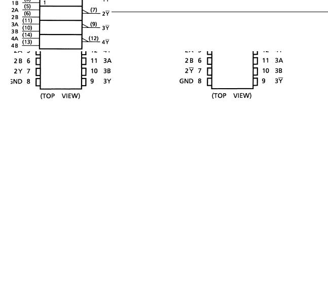
Pin Assignment
TC74AC257 |
TC74AC258 |
IEC Logic Symbol
TC74AC257 |
TC74AC258 |
Truth Table
|
|
|
Inputs |
|
|
Outputs |
|
||||
|
|
|
|
|
|
|
|
|
|
|
|
|
OE |
|
SELECT |
|
A |
B |
Y (257) |
|
Y |
|
(258) |
|
H |
X |
|
X |
X |
Z |
|
|
|
Z |
|
|
|
|
|
|
|
|
|
|
|||
|
L |
L |
|
L |
X |
L |
|
|
|
H |
|
|
|
|
|
|
|
|
|
|
|||
|
L |
L |
|
H |
X |
H |
|
|
|
L |
|
|
|
|
|
|
|
|
|
|
|||
|
L |
H |
|
X |
L |
L |
|
|
|
H |
|
|
|
|
|
|
|
|
|
|
|||
|
L |
H |
|
X |
H |
H |
|
|
|
L |
|
|
|
|
|
|
|
|
|
|
|
|
|
X: Don’t care
Z: High impedance
2 |
2007-10-01 |

TC74AC257,258P/F/FN
System Diagram
TC74AC257 |
TC74AC258 |
Absolute Maximum Ratings (Note 1)
Characteristics |
Symbol |
Rating |
Unit |
|
|
|
|
Supply voltage range |
VCC |
−0.5~7.0 |
V |
DC input voltage |
VIN |
−0.5~VCC + 0.5 |
V |
DC output voltage |
VOUT |
−0.5~VCC + 0.5 |
V |
Input diode current |
IIK |
±20 |
mA |
Output diode current |
IOK |
±50 |
mA |
DC output current |
IOUT |
±50 |
mA |
DC VCC/ground current |
ICC |
±100 |
mA |
Power dissipation |
PD |
500 (DIP) (Note 2)/180 (SOP) |
mW |
Storage temperature |
Tstg |
−65~150 |
°C |
Note 1: Exceeding any of the absolute maximum ratings, even briefly, lead to deterioration in IC performance or even destruction.
Using continuously under heavy loads (e.g. the application of high temperature/current/voltage and the significant change in temperature, etc.) may cause this product to decrease in the reliability significantly even if the operating conditions (i.e. operating temperature/current/voltage, etc.) are within the absolute maximum ratings and the operating ranges.
Please design the appropriate reliability upon reviewing the Toshiba Semiconductor Reliability Handbook (“Handling Precautions”/Derating Concept and Methods) and individual reliability data (i.e. reliability test report and estimated failure rate, etc).
Note 2: 500 mW in the range of Ta = −40~65°C. From Ta = 65 to 85°C a derating factor of −10 mW/°C should be applied up to 300 mW.
3 |
2007-10-01 |
 Loading...