


TA8227P
TOSHIBA Bipolar Linear Integrated Circuit Silicon Monolithic
TA8227P
Low Frequency Power Amplifier |
|
TA8227P is an audio power IC with built-in two channels |
|
developed for portable radio cassette tape recorder with power |
|
ON/OFF switch. |
|
Because of the parts reduction and DIP (Dual Inline Package), |
|
space merit is remarkable. |
|
Thermal shut down protection circuit is built in. |
|
Features |
|
· High power |
|
: Pout = 2.5 W/CH (typ.) |
|
(VCC = 9 V, RL = 4 Ω, f = 1 kHz, THD = 10%) |
Weight: 1.4 g (typ.) |
:Pout = 3.0 W/CH (typ.)
(VCC = 9 V, RL = 3 Ω, f = 1 kHz, THD = 10%)
·Voltage gain
:Gv = 45.0dB (typ.) (Rf = 120 Ω, f = 1 kHz)
:Gv = 56.5dB (typ.) (Rf = 0 Ω, f = 1 kHz)
·Small quiescent current
:ICCQ = 21 mA (typ.) (VCC = 9 V, Vin = 0)
·Ripple rejection ratio
:R.R. = −52dB (typ.) (VCC = 9 V, fripple = 100 Hz, Rg = 600 Ω)
·Cross Talk
:C.T. = −50dB (typ.) (VCC = 9 V, f = 1 kHz, Rg = 600 Ω)
·Output noise voltage
:Vno = 0.3 mVrms (typ.) (VCC = 9 V, Rg = 10 kΩ, BW = 20 Hz~20 kHz)
·Stand-by switch
·Soft clip
·Built-in thermal shut down protection circuit
·Operation supply voltage range: VCC (opr) = 5~12 V (Ta = 25°C)
·Low popping noise at power ON
·Best for supply voltage 9 V
1 |
2002-03-05 |

TA8227P
Block Diagram
Application Information and Application Method
1. Adjustment of voltage gain
The voltage gain Gv is obtained as follows by R1, R2 and Rf in Figure 1.
Gv = 20 log Rf + R1 + R2
Rf + R1
When Rf = 0 Ω |
Gv = 56.5dB (typ.) |
When Rf = 120 Ω |
Gv = 45dB (typ.) |
Figure 1
By increasing Rf, reduction of Gv is possible. However, since the feedback increase is liable to produce oscillation, it is recommended to use this at 40dB or over.
2. Thermal shut-down circuit
The thermal shut-down circuit is built in for the purpose of preventing the destruction of IC due to the abnormal temperature rise when the heat radiation is insufficient.
The operation temperature is set at radiation Fin temperature 175°C (typ.).
At this temperature or over the bias is interrupted to prevent the destruction of IC.
2 |
2002-03-05 |
TA8227P
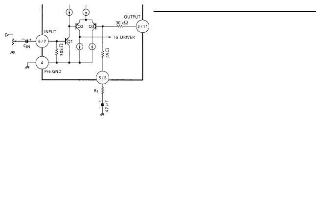
3. Input stage
The input circuit of this IC is as shown in Figure 2.
PNP Tr: Q1 is provided in the input circuit so as to make its usage possible without the input coupling capacitor.
However, at pin 6 and 7, max 60 mV offset voltage is produced. Application after checking volume slide noise is recommended.
For cutting the volume slide noise, insert the input capacitor: CIN in series to interrupt the DC component.
Figure 2
4. Oscillation preventive measures (Note 1)
For oscillation preventive capacitor C6 and C7 between the output terminal and GND, it is recommended to use polyester film capacitor having good characteristics for temperature and for high frequency.
Since the characteristics of the capacitor is liable to be influenced by the temperature, use this capacitor after the temperature test to check the oscillation allowance.
In addition, as the position of the electrolytic capacitor has a remarkable influence on the oscillation, connect C10 to VCC at the nearest possible position from power GND.
At using this application with the voltage gain reduced, oscillation is liable to be produced. Apply the capacitor after checking enough for its capacity, type and mounting position.
Note 1: As the oscillation allowance varies according to the printed pattern layout, the standard printed board of TOSHIBA is recommended to be referred to design it.
5. Power ON/OFF switch
There is power ON/OFF switch at pin 1. However, output power is changed by pin 1 supply voltage when pin 1 supply voltage is not same pin 12 supply voltage, after referring to attached data, select pin 1 supply voltage.
6. Input voltage
When the excessive signal is input, turning-up is produced in the clip waveform. The turning-up point is Vin = 300 mVrms (typ.) : VCC = 9 V, RL = 4 Ω, f = 1 kHz: Enough care must be taken for this phenomenon.
3 |
2002-03-05 |

TA8227P
Maximum Ratings (Ta = 25°C)
Characteristics |
Symbol |
Rating |
Unit |
|
|
|
|
DC supply voltage |
VCC |
20 |
V |
Output current (peak/CH) |
IO (peak) |
2.5 |
A |
Power dissipation |
PD (Note 2) |
4.0 |
W |
Operating temperature |
Topr |
−20~75 |
°C |
Storage temperature |
Tstg |
−55~150 |
°C |
Note 2: Value for mounting on PC board (refer to PD − Ta curve)
Electrical Characteristics
(unless otherwise specified, VCC = 9 V, RL = 4 Ω, Rg = 600 Ω, f = 1 kHz, Ta = 25°C)
Characteristics |
Symbol |
Test |
Test Condition |
Min |
Typ. |
Max |
Unit |
|
Circuit |
||||||||
|
|
|
|
|
|
|
||
Quiescent current |
ICCQ |
― |
Vin = 0 |
― |
21 |
45 |
mA |
|
Output power |
Pout (1) |
― |
THD = 10% |
2.0 |
2.5 |
― |
W |
|
Pout (2) |
― |
THD = 10%, RL = 3 Ω |
― |
3.0 |
― |
|||
|
|
|||||||
Total harmonic distortion |
THD |
― |
Pout = 0.4 W/CH |
― |
0.2 |
1.0 |
% |
|
|
Gv (1) |
― |
Rf = 120 Ω, |
43 |
45 |
47 |
|
|
Voltage gain |
VOUT = 0.775 Vrms (0dBm) |
dB |
||||||
Gv (2) |
― |
Rf = 0 Ω, |
― |
56.5 |
― |
|||
|
|
|||||||
|
VOUT = 0.775 Vrms (0dBm) |
|
||||||
Input resistance |
RIN |
― |
― |
― |
30 |
― |
kΩ |
|
Output noise voltage |
Vno |
― |
Rg = 10 kΩ, |
― |
0.3 |
1.0 |
mVrms |
|
BW = 20 Hz~20 kHz |
||||||||
Ripple rejection ratio |
R.R. |
― |
Rg = 600 Ω, fripple = 100 Hz |
― |
−52 |
― |
dB |
|
Cross talk |
C.T. |
― |
Rg = 600 Ω, |
― |
−50 |
― |
dB |
|
VOUT = 0.775 Vrms (0dBm) |
||||||||
Input offset voltage |
V6, V7 |
― |
― |
― |
30 |
60 |
mV |
|
Stand-by current |
Istb |
― |
SW1 → OFF |
― |
1 |
― |
µA |
|
|
|
|
|
|
|
|
|
TYP. DC Voltage of Each Terminal (VCC = 9 V, Ta = 25°C)
Terminal No. |
1 |
2 |
3 |
4 |
5 |
6 |
7 |
8 |
9 |
10 |
11 |
12 |
|
|
|
|
|
|
|
|
|
|
|
|
|
DC Voltage (V) |
VCC |
4.5 |
8.7 |
GND |
0.7 |
0.03 |
0.03 |
0.7 |
5.0 |
8.7 |
4.5 |
VCC |
4 |
2002-03-05 |
 Loading...