


TB6600HG
TOSHIBA BiCD Integrated Circuit Silicon Monolithic
TB6600HG
PWM Chopper-Type bipolar
Stepping Motor Driver IC
The TB6600HG is a PWM chopper-type single-chip bipolar sinusoidal |
|
||
TB6600HG |
|||
micro-step stepping motor driver. |
|
||
Forward and reverse rotation control is available |
with 2-phase, |
||
1-2-phase, W1-2-phase, 2W1-2-phase, and 4W1-2-phase excitation |
|||
modes. |
|
|
|
2-phase bipolar-type stepping motor can be driven by only clock signal |
|||
with low vibration and high efficiency. |
|
|
|
Features |
|
||
• |
Single-chip bipolar sinusoidal micro-step stepping motor driver |
HZIP25-P-1.00F |
|
• Ron (upper + lower) = 0.4 Ω (typ.) |
|
||
Weight: |
|||
|
Forward and reverse rotation control available |
||
• |
HZIP25-P-1.00F: 7.7g (typ.) |
||
• Selectable phase drive (1/1, 1/2, 1/4, 1/8, and 1/16 step) |
|
||
• Output withstand voltage: Vcc = 50 V |
|
||
• Output current: IOUT = 5.0 A (absolute maximum ratings, peak) |
|
||
|
IOUT = 4.5 A (operating range, maximal value) |
|
|
• |
Packages: HZIP25-P-1.00F |
|
|
• Built-in input pull-down resistance: 100 kΩ (typ.), (only TQ terminal: 70Ω(typ.))
•Output monitor pins (ALERT): Maximum of IALERT = 1 mA
•Output monitor pins (MO): Maximum of IMO = 1 mA
•Equipped with reset and enable pins
•Stand by function
•Single power supply
•Built-in thermal shutdown (TSD) circuit
•Built-in under voltage lock out (UVLO) circuit
•Built-in over-current detection (ISD) circuit
1 |
2014-01-30 |
|
|
|
|
|
|
|
|
|
|
|
|
TB6600HG |
|
|
|
|
|
|
|
|
|
|
|
|
|
|
|
|
|
|
|
|
|
|
|
|
|
|
|
|
|
|
|
|
|
|
|
|
|
|
|
|
|
|
|
|
|
|
|
|
|
|
|
|
|
Pin Functions |
|
|
|
||||||||
|
|
|
|
|
|
|
|
|
|
|||
|
|
Pin No. |
|
|
|
I/O |
Symbol |
Functional Description |
Remark |
|||
|
|
|
|
|
|
|
|
|
|
|||
|
1 |
|
|
|
|
Output |
ALERT |
TSD / ISD monitor pin |
Pull-up by external resistance |
|||
|
|
|
|
|
|
|
|
|
|
|||
|
2 |
|
|
|
|
― |
SGND |
Signal ground |
|
|||
|
|
|
|
|
|
|
|
|
|
|||
|
3 |
|
|
|
|
Input |
TQ |
Torque (output current) setting input pin |
|
|||
|
|
|
|
|
|
|
|
|
|
|||
|
|
4 |
|
|
|
|
Input |
Latch/Auto |
Select a return type for TSD. |
L: Latch, H: Automatic return |
||
|
|
|
|
|
|
|
|
|
|
|||
|
|
5 |
|
|
|
|
Input |
Vref |
Voltage input for 100% current level |
|
||
|
|
|
|
|
|
|
|
|
|
|||
|
|
6 |
|
|
|
|
Input |
Vcc |
Power supply |
|
||
|
|
|
|
|
|
|
|
|
|
|||
|
|
7 |
|
|
|
|
Input |
M1 |
Excitation mode setting input pin |
|
||
|
|
|
|
|
|
|
|
|
|
|||
|
|
8 |
|
|
|
|
Input |
M2 |
Excitation mode setting input pin |
|
||
|
|
|
|
|
|
|
|
|
|
|||
|
|
9 |
|
|
|
|
Input |
M3 |
Excitation mode setting input pin |
|
||
|
|
|
|
|
|
|
|
|
|
|||
|
|
10 |
|
|
|
|
Output |
OUT2B |
B channel output 2 |
|
||
|
|
|
|
|
|
|
|
|
|
|||
|
|
11 |
|
|
|
|
― |
NFB |
B channel output current detection pin |
|
||
|
|
12 |
|
|
|
|
Output |
OUT1B |
B channel output 1 |
|
||
|
|
|
|
|
|
|
|
|
|
|||
|
|
13 |
|
|
|
|
― |
PGNDB |
Power ground |
|
||
|
|
|
|
|
|
|
|
|
|
|||
|
|
14 |
|
|
|
|
Output |
OUT2A |
A channel output 2 |
|
||
|
|
|
|
|
|
|
|
|
|
|||
|
|
15 |
|
|
|
|
― |
NFA |
A channel output current detection pin |
|
||
|
|
16 |
|
|
|
|
Output |
OUT1A |
A channel output 1 |
|
||
|
|
|
|
|
|
|
|
|
|
|||
|
|
17 |
|
|
|
|
― |
PGNDA |
Power ground |
|
||
|
|
|
|
|
|
|
|
|
|
|||
|
|
18 |
|
|
|
|
Input |
ENABLE |
Enable signal input pin |
H: Enable, L: All outputs off |
||
|
|
|
|
|
|
|
|
|
|
|||
|
|
19 |
|
|
|
|
Input |
RESET |
Reset signal input pin |
L: Initial mode |
||
|
|
|
|
|
|
|
|
|
|
|||
|
|
20 |
|
|
|
|
Input |
Vcc |
Power supply |
|
||
|
|
|
|
|
|
|
|
|
|
|||
|
|
21 |
|
|
|
|
Input |
CLK |
CLK pulse input pin |
|
||
|
|
|
|
|
|
|
|
|
|
|||
|
|
22 |
|
|
|
|
Input |
CW/CCW |
Forward/reverse control pin |
L: CW, H:CCW |
||
|
|
|
|
|
|
|
|
|
|
|||
|
|
23 |
|
|
|
|
― |
OSC |
Resistor connection pin for internal oscillation setting |
|
||
|
|
|
|
|
|
|
|
|
|
|
|
|
|
|
24 |
|
|
|
|
Output |
Vreg |
Control side connection pin for power capacitor |
Connecting capacitor to |
||
|
|
|
|
|
SGND |
|||||||
|
|
|
|
|
|
|
|
|
|
|
|
|
|
|
25 |
|
|
|
|
Output |
MO |
Electrical angle monitor pin |
Pull-up by external resistance |
||
|
|
|
|
|
|
|
|
|
|
|
|
|
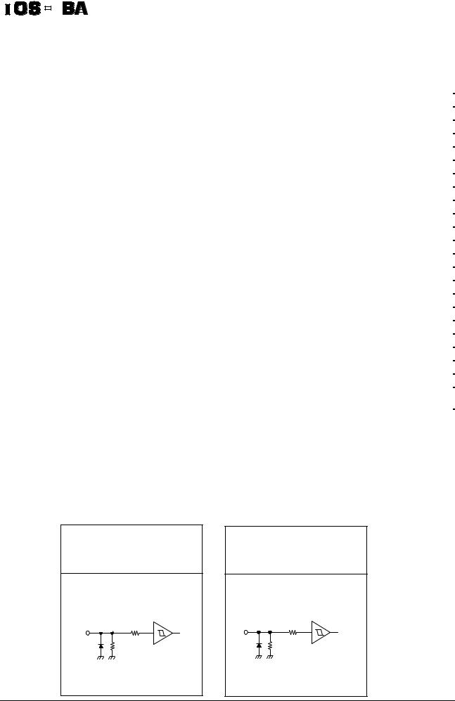
<Terminal circuits>
Input pins |
Input pins |
(M1, M2, M3,CLK, CW/CCW, |
(TQ) |
ENABLE, RESET, Latch/Auto) |
|
|
VDD |
10kΩ |
10kΩ |
100kΩ |
70kΩ |
2 |
2014-01-30 |

TB6600HG
Pin Assignment
Top View
SGND |
Latch/Auto |
Vcc |
M2 |
OUT2B |
OUT1B |
OUT2A |
OUT1A |
ENABLE |
Vcc |
CW/CCW |
Vreg |
2 |
4 |
6 |
8 |
10 |
12 |
14 |
16 |
18 |
20 |
22 |
24 |
|
|
|
|
|
|
|
|
|
|
|
|
|
|
|
|
|
|
|
|
|
|
|
|
|
|
|
|
|
|
|
|
|
|
|
|
|
|
|
|
|
|
|
|
|
|
|
|
|
|
|
|
|
|
|
|
|
|
|
|
|
|
|
|
|
|
|
|
|
|
|
|
|
|
|
|
|
|
|
|
|
|
|
|
|
|
|
|
|
|
|
|
|
|
|
|
|
|
|
|
|
|
|
|
|
|
|
|
|
|
|
|
|
|
|
|
|
|
|
|
|
|
|
|
|
|
|
|
|
|
|
|
|
|
|
|
|
|
|
|
|
|
|
|
|
|
|
|
|
|
|
|
|
|
|
|
|
|
|
|
|
|
|
|
|
|
|
|
|
|
|
|
|
|
|
|
|
|
|
|
|
|
|
|
|
|
|
|
|
|
|
|
|
|
|
|
|
|
|
|
|
|
|
|
|
|
|
|
|
|
|
|
|
|
|
|
|
|
|
|
|
|
|
|
|
|
|
|
|
|
|
|
|
|
|
|
|
|
|
|
|
|
|
|
|
|
|
|
|
|
|
|
|
|
|
|
|
|
|
|
|
|
|
|
|
|
|
1 |
|
3 |
|
5 |
|
7 |
|
9 |
|
11 |
13 |
15 |
17 |
19 |
21 |
23 |
25 |
|||||||||||||||||||||||||||||||||
ALERT |
|
TQ |
|
Vref |
|
M1 |
|
M3 |
|
NFB |
|
PGNDB |
|
NFA |
|
PGNDA |
|
RESET |
|
CLK |
|
OSC |
|
MO |
||||||||||||||||||||||||||
3 |
2014-01-30 |
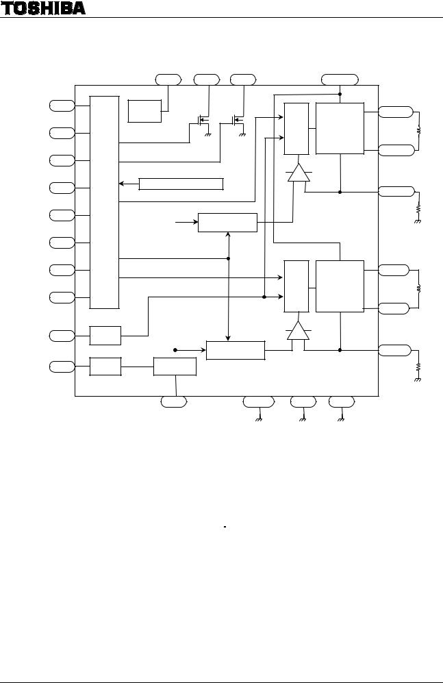
TB6600HG
Block Diagram
|
|
|
Vreg |
MO |
ALERT |
|
Vcc |
|
|
|
|
24 |
25 |
1 |
|
6, 20 |
|
M1 |
7 |
|
Reg(5V) |
|
|
|
|
OUT1A |
|
|
|
|
16 |
|
|||
|
|
|
|
|
|
|
||
|
|
|
|
|
|
|
|
|
|
|
|
|
|
|
Pre |
H-Bridge |
|
M2 |
8 |
|
|
|
|
-drive |
driver A |
|
|
|
|
|
|
|
|
|
|
|
9 |
|
|
|
|
|
14 |
|
M3 |
|
|
|
|
|
|
OUT2A |
|
|
|
|
|
|
|
|
|
|
CW/CCW |
22 |
|
TSD / ISD / UVLO |
|
|
15 |
NFA |
|
Input |
|
|
|
|
||||
|
|
|
|
|
|
|
||
|
|
|
|
|
|
|
|
|
CLK |
21 |
circuit |
|
|
|
|
|
|
|
|
Current selector |
|
|
|
|||
|
|
|
|
|
circuit A |
|
|
|
RESET |
19 |
|
|
|
|
|
|
|
ENABLE |
18 |
|
|
|
|
|
12 |
OUT1B |
|
|
|
|
|
|
|||
|
|
|
|
|
|
Pre |
H-Bridge |
|
Latch/Auto |
4 |
|
|
|
|
-drive |
driver B |
|
|
|
|
|
|
|
|||
|
|
|
|
|
|
|
10 |
OUT2B |
|
|
|
|
|
|
|
|
|
OSC |
23 |
OSC |
|
|
|
|
|
NFB |
|
|
|
|
Current selector |
|
11 |
||
|
|
|
|
|
circuit B |
|
|
|
|
|
1/3 |
100%/30% |
|
|
|
|
|
Vref |
5 |
|
|
|
|
|
||
|
|
|
|
|
|
|
||
|
|
|
3 |
|
2 |
17 |
13 |
|
|
|
|
TQ |
|
|
|
|
|
|
|
|
|
|
SGND |
PGNDA |
PGNDB |
|
Setting of Vref
Input |
Voltage ratio |
|
TQ |
||
|
||
|
|
|
L |
30% |
|
|
|
|
H |
100% |
|
|
|
4 |
2014-01-30 |

TB6600HG
Description of Functions
1. Excitation Settings
The excitation mode can be selected from the following eight modes using the M1, M2 and M3 inputs. New excitation mode starts from the initial mode when M1, M2, or M3 inputs are shifted during motor operation. In this case, output current waveform may not continue.
|
Input |
|
Mode |
|
M1 |
M2 |
M3 |
(Excitation) |
|
|
|
|
|
|
L |
L |
L |
Standby mode |
|
(Operation of the internal circuit is almost turned off.) |
||||
|
|
|
||
|
|
|
|
|
L |
L |
H |
1/1 (2-phase excitation, full-step) |
|
|
|
|
|
|
L |
H |
L |
1/2A type (1-2 phase excitation A type) |
|
( 0%, 71%, 100% ) |
||||
|
|
|
||
|
|
|
|
|
L |
H |
H |
1/2B type (1-2 phase excitation B type) |
|
( 0%, 100% ) |
||||
|
|
|
||
|
|
|
|
|
H |
L |
L |
1/4 (W1-2 phase excitation) |
|
|
|
|
|
|
H |
L |
H |
1/8 (2W1-2 phase excitation) |
|
|
|
|
|
|
H |
H |
L |
1/16 (4W1-2 phase excitation) |
|
|
|
|
|
|
H |
H |
H |
Standby mode |
|
(Operation of the internal circuit is almost turned off.) |
||||
|
|
|
||
|
|
|
|
Note: To change the exciting mode by changing M1, M2, and M3, make sure not to set M1 = M2 = M3 = L or M1 = M2 = M3 = H.
Standby mode
The operation mode moves to the standby mode under the condition M1 = M2 = M3 = L or M1 = M2 = M3 = H.
The power consumption is minimized by turning off all the operations except protecting operation. In standby mode, output terminal MO is HZ.
Standby mode is released by changing the state of M1=M2=M3=L and M1=M2=M3=H to other state. Input signal is not accepted for about 200 μs after releasing the standby mode.
5 |
2014-01-30 |

TB6600HG
2. Function
(1)To turn on the output, configure the ENABLE pin high. To turn off the output, configure the ENABLE pin low.
(2)The output changes to the Initial mode shown in the table below when the ENABLE signal goes High level and the RESET signal goes Low level. (In this mode, the status of the CLK and CW/CCW pins are irrelevant.)
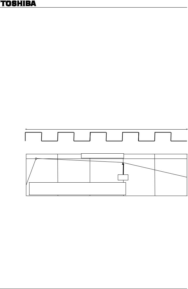
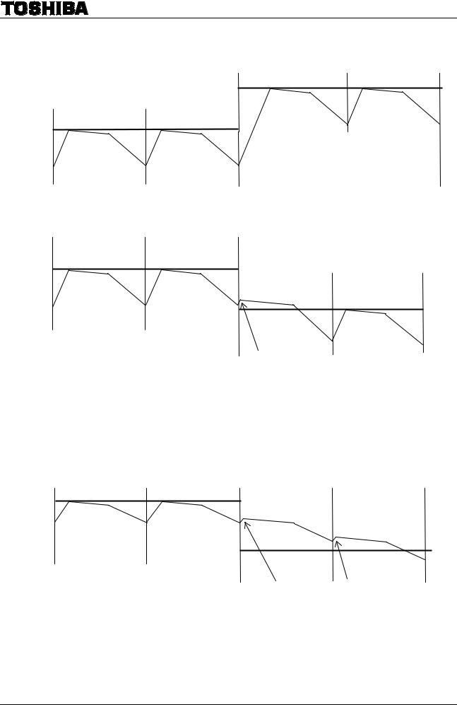
(3)As shown in the below figure of Example 1, when the ENABLE signal goes Low level, it sets an OFF on the output. In this mode, the output changes to the initial mode when the RESET signal goes Low level. Under this condition, the initial mode is output by setting the ENABLE signal High level. And the motor operates from the initial mode by setting the RESET signal High level.
(Example 1)
1
CLK
RESET
ENABLE
Internal current set
Output current(*)(phase A ) (A )
Z
(*: Output current starts rising at the timing of PWM frequency just after ENABLE pin outputs high.)
|
|
|
|
|
|
|
|
Command of the standby has a higher priority |
|
|
|
|
|
Input |
|
|
|||
|
|
|
|
|
Output mode |
than ENABLE. Standby mode can be turned on |
|||
|
CLK |
CW/CCW |
RESET |
ENABLE |
|||||
|
|
and off regardless of the state of ENABLE. |
|||||||
|
|
|
|
|
|
|
|
||
|
|
|
|
L |
H |
H |
CW |
X: |
Don’t Care |
|
|
|
|
||||||
|
|
|
|
||||||
|
|
|
|
|
|
|
|
|
|
|
|
|
|
H |
H |
H |
CCW |
|
|
|
|
|
|
|
|
||||
|
|
|
|
|
|
||||
|
|
|
|
|
|
|
|
|
|
|
X |
X |
L |
H |
Initial mode |
|
|
||
|
|
|
|
|
|
|
|
|
|
|
X |
X |
X |
L |
Z |
|
|
||
|
|
|
|
|
|
|
|
|
|
6 |
2014-01-30 |
|
|
TB6600HG |
3. Initial Mode |
|
|
When RESET is used, the phase currents are as follows. |
|
|
Excitation Mode |
Phase A Current |
Phase B Current |
1/1 (2-phase excitation, full-step) |
100% |
-100% |
1/2A type (1-2 phase excitation A type) (0%, 71%, 100%) |
100% |
0% |
1/2B type (1-2 phase excitation B type) (0%, 100%) |
100% |
0% |
1/4 (W1-2 phase excitation) |
100% |
0% |
1/8 (2W1-2 phase excitation) |
100% |
0% |
1/16 (4W1-2 phase excitation) |
100% |
0% |
current direction is defined as follows. OUT1A → OUT2A: Forward direction OUT1B → OUT2B: Forward direction
4. 100% current settings (Current value)
100% current value is determined by Vref inputted from external part and the external resistance for detecting output current. Vref is doubled 1/3 inside IC.
Io (100%) = (1/3 × Vref) ÷ RNF
The average current is lower than the calculated value because this IC has the method of peak current detection.
Pleas use the IC under the conditions as follows; 0.11Ω ≤ RNF ≤ 0.5Ω, 0.3V ≤ Vref ≤ 1.95V
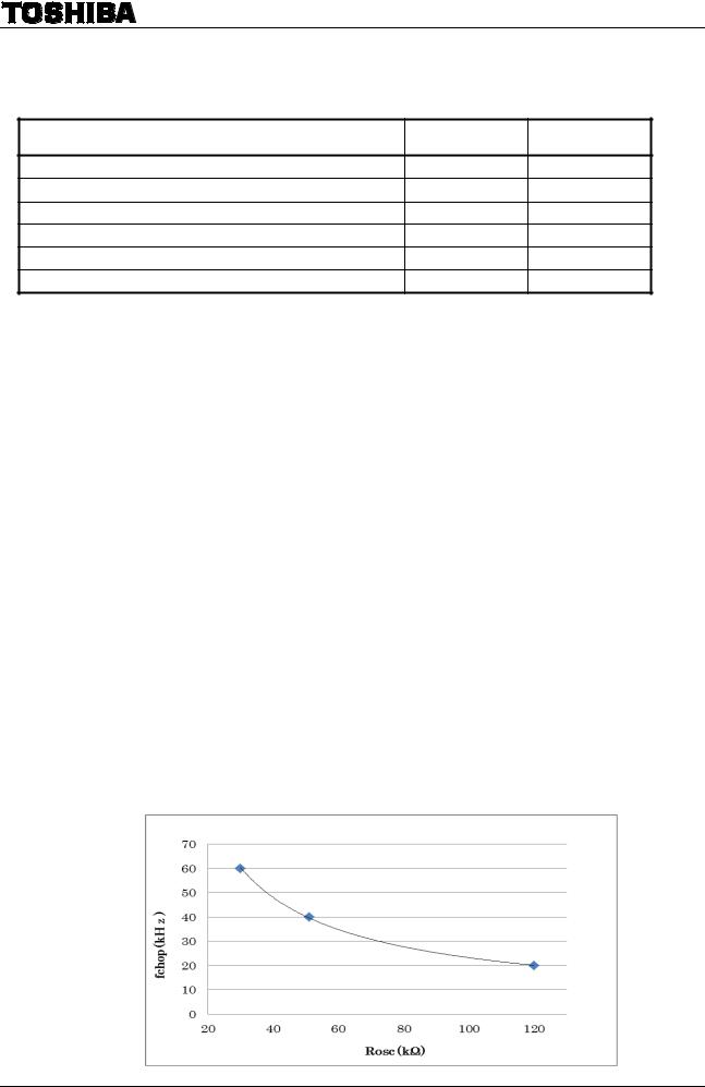
5.OSC
Triangle wave is generated internally by CR oscillation by connecting external resistor to OSC terminal. Rosc should be from 30kΩ to 120kΩ. The relation of Rosc and fchop is shown in below table and figure. The values of fchop of the below table are design guarantee values. They are not tested for pre-shipment.
Rosc(kΩ) |
|
fchop(kHz) |
|
|
Min |
Typ. |
Max |
30 |
- |
60 |
- |
51 |
- |
40 |
- |
120 |
- |
20 |
- |
7 |
2014-01-30 |
TB6600HG
6. Decay Mode
It takes approximately five OSCM cycles for charging-discharging a current in PWM mode. The 40% fast decay mode is created by inducing decay during the last two cycles in Fast Decay mode.
The ratio 40% of the fast decay mode is always fixed.
The relation between the master clock frequency (fMCLK), the OSCM frequency (fOSCM) and the PWM frequency (fchop) is shown as follows:
fOSCM = 1/20 ×fMCLK fchop = 1/100 ×fMCLK
When Rosc=51kΩ, the master clock=4MHz, OSCM=200kHz, the frequency of PWM(fchop)=40kHz.
6-1. Current Waveform and Mixed Decay Mode settings
The period of PWM operation is equal to five periods of OSCM. The ratio 40% of the fast decay mode is always fixed.
The “NF” refers to the point at which the output current reaches its predefined current level.
MDT means the point of MDT (MIXED DECAY TIMMING) in the below diagram.
fchop
OSCM
Internal Waveform
|
Predefined Current Level |
40% |
NF |
|
|
fast |
|
Decay |
MDT |
Mode |
Charge mode → NF: Predefined current level → Slow mode → MDT(Mixed decay timing) → Fast mode → Current monitoring → (When predefined current level Output current) Charge mode
8 |
2014-01-30 |
TB6600HG
6-2. Effect of Decay Mode
•Increasing the current (sine wave)
Predefined |
Slow |
Slow |
Current Level |
Fast |
Fast |
|
||
|
|
Charge |
Predefined |
Slow |
Slow |
Charge |
Current Level |
|
|
|
Fast |
|
Fast |
|
|
|
||
|
Charge |
Charge |
|
•Decreasing the current (In case the current is decreased to the predefined value in a short time because it decays quickly.)
Predefined |
Slow |
Slow |
|
|
|
Current Level |
Fast |
Fast |
|
|
|
|
|
|
|
||
|
Charge |
Charge |
Slow |
|
|
|
|
Predefined |
Slow |
|
|
|
|
|
|
||
|
|
Current Level |
Fast |
|
Fast |
|
|
|
Charge |
||
|
|
|
|
|
Charge
Even if the output current rises above the predefined current at the RNF point, the current control mode is briefly switched to Charge mode for current sensing.
•Decreasing the current (In case it takes a long time to decrease the current to the predefined value because the current decays slowly.)
Predefined |
Slow |
Slow |
|
Current Level |
Fast |
Fast |
|
|
Slow |
||
|
Charge |
|
|
|
|
Fast |
|
|
|
|
|
|
|
|
Slow |
|
|
Predefined |
Fast |
|
|
|
|
|
|
Current Level |
|
Charge Charge
Even if the output current rises above the predefined current at the RNF point, the current control mode is briefly switched to Charge mode for current sensing.
During Mixed Decay and Fast Decay modes, if the predefined current level is less than the output current at the RNF (current monitoring point), the Charge mode in the next chopping cycle will disappear (though the current control mode is briefly switched to Charge mode in actual operations for current sensing) and the current is controlled in Slow and Fast Decay modes (mode switching from Slow Decay mode to Fast Decay mode at the MDT point).
Note: The above figures are rough illustration of the output current. In actual current waveforms, transient response curves can be observed.
9 |
2014-01-30 |

TB6600HG
6-3. Current Waveforms in Mixed Decay Mode
|
fchop |
fchop |
OSCM |
|
|
Internal |
|
|
waveform |
|
|
IOUT |
|
Predefined Current Level |
|
NF |
|
|
|
|
Predefined |
|
|
Current Level |
NF |
|
|
|
|
40% |
|
|
Fast |
|
|
DECAY |
|
|
MODE |
|
|
MDT (MIXED DECAY TIMMING) points
• When the NF points come after Mixed Decay Timing points
Switches to Fast mode after Charge mode
|
fchop |
fchop |
|
|
Predefined |
|
|
Current Level |
IOUT |
|
NF |
|
|
MDT (MIXED DECAY TIMMING) points |
Predefined |
NF |
|
|
|
|
Current Level |
|
|
40% |
|
|
Fast |
|
|
DECAY |
|
|
MODE |
|
|
CLK signal input
•When the output current value > predefined current level in Mixed Decay mode
|
fchop |
fchop |
fchop |
Predefined |
|
|
|
Current |
NF |
|
|
Level |
|
|
|
|
|
|
|
IOUT |
|
|
|
|
|
NF |
|
|
|
Predefined Current |
|
|
|
Level |
|
40% |
|
|
|
Fast |
|
|
|
DECAY |
|
MDT (MIXED DECAY TIMMING) points |
|
MODE |
|
|
|
CLK signal input
Even if the output current rises above the predefined current at the RNF point, the current control mode is briefly switched to Charge mode for current sensing.
10 |
2014-01-30 |
TB6600HG
Output Stage Transistor Operation Mode
|
Vcc |
U1 |
|
ON |
Note |
OUT1 |
Load OUT2 |
OFF |
|
L1 |
|
RNF |
|
|
PGND |
Charge Mode |
|
Vcc
U2 |
U1 |
|
U2 |
OFF |
OFF |
Note |
OFF |
|
OUT1 |
Load OUT2 |
|
ON |
ON |
|
L2 |
L2 |
L1 |
|
ON |
|
RNF |
|
|
|
|
PGND |
|
|
|
Slow Mode |
|
|
Vcc |
|
U1 |
|
U2 |
OFF |
Note |
ON |
|
OUT1 Load |
OUT2 |
L1 |
|
L2 |
ON |
|
OFF |
RNF
PGND
Fast Mode
Output Stage Transistor Operation Functions
CLK |
U1 |
U2 |
L1 |
L2 |
|
|
|
|
|
CHARGE |
ON |
OFF |
OFF |
ON |
|
|
|
|
|
SLOW |
OFF |
OFF |
ON |
ON |
|
|
|
|
|
FAST |
OFF |
ON |
ON |
OFF |
|
|
|
|
|
Note: The above chart shows an example of when the current flows as indicated by the arrows in the above figures. If the current flows in the opposite direction, refer to the following chart:
CLK |
U1 |
U2 |
L1 |
L2 |
|
|
|
|
|
CHARGE |
OFF |
ON |
ON |
OFF |
|
|
|
|
|
SLOW |
OFF |
OFF |
ON |
ON |
|
|
|
|
|
FAST |
ON |
OFF |
OFF |
ON |
|
|
|
|
|
Upon transitions of above-mentioned functions, a dead time of about 300 ns (Design guarantee value) is inserted respectively.
11 |
2014-01-30 |
 Loading...