


 Loading...
TC74AC166P/F/FN
TOSHIBA CMOS Digital Integrated Circuit Silicon Monolithic
TC74AC166P,TC74AC166F,TC74AC166FN
8-Bit Shift Register (P-IN, S-OUT)
The TC74AC166 is an advanced high speed CMOS 8-BIT PARALLEL/SERIAL-IN, SERIAL-OUT SHIFT REGISTER fabricated with silicon gate and double-layer metal wiring C2MOS technology.
It achieves the high speed operation similar to equivalent Bipolar Schottky TTL while maintaining the CMOS low power dissipation.
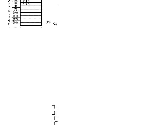
It consists of parallel-in or serial-in, serial-out 8-bit shift register with a gated clock input and an overriding clear input. The parallel-in or serial-in modes are controlled by the SHIFT/ LOAD input. When the SHIFT/ LOAD input is held high, the serial data input is enabled and the eight flip-flops perform serial shifting on each clock pulse. When held low, the
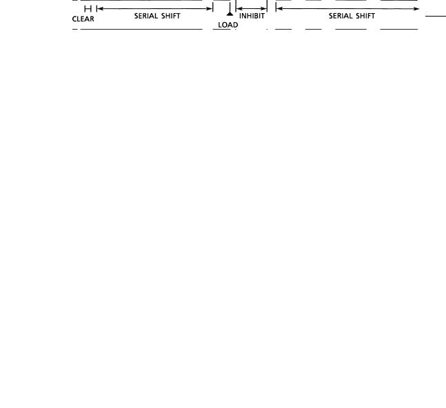
parallel data inputs are enabled and synchronous loading occurs on the next clock pulse. Clocking is accomplished on the low-to-high transition of the clock pulse. The CLOCK-INHIBIT input should be shifted high only while the CLOCK input is held high. A direct clear input overrides all other inputs, including the clock, and sets all the flip-flops to zero. Functional details are shown in the truth table and the timing charts.
All inputs are equipped with protection circuits against static discharge or transient excess voltage.
Features
•High speed: fmax = 170 MHz (typ.) at VCC = 5 V
•Low power dissipation: ICC = 8 μA (max) at Ta = 25°C
•High noise immunity: VNIH = VNIL = 28% VCC (min)
•Symmetrical output impedance: |IOH| = IOL = 24 mA (min)
Capability of driving 50 Ω transmission lines.
•Balanced propagation delays: tpLH − tpHL
•Wide operating voltage range: VCC (opr) = 2 to 5.5 V
•Pin and function compatible with 74HC166
Note: xxxFN (JEDEC SOP) is not available in Japan.
TC74AC166P
TC74AC166F
TC74AC166FN
Weight |
|
DIP16-P-300-2.54A |
: 1.00 g (typ.) |
SOP16-P-300-1.27A |
: 0.18 g (typ.) |
SOL16-P-150-1.27 |
: 0.13 g (typ.) |
Pin Assignment
1 |
2007-10-01 |
TC74AC166P/F/FN
IEC Logic Symbol
Truth Table
|
|
|
|
|
Inputs |
|
|
Internal |
Output |
||
|
|
|
|
|
|
|
Output |
||||
|
|
|
|
|
|
|
|
|
|
||
|
|
|
SHIFT/ |
CK INH. |
|
CK |
SERIAL |
PARALLEL |
QA |
QB |
QH |
CLR |
|
||||||||||
LOAD |
|
IN |
A H |
||||||||
|
|
|
|
|
|
|
|
|
|||
|
L |
X |
X |
|
X |
X |
X |
L |
L |
L |
|
|
|
|
|
|
|
|
|
|
|
|
|
|
H |
X |
X |
|
|
X |
X |
|
No Change |
||
|
|
|
|
|
|
|
|
|
|
|
|
|
H |
L |
L |
|
|
X |
a h |
a |
b |
h |
|
|
|
|
|
|
|
|
|
|
|
||
|
H |
H |
L |
|
|
H |
X |
H QAn |
QGn |
||
|
|
|
|
|
|
|
|
|
|
|
|
|
H |
H |
L |
|
|
L |
X |
L |
QAn |
QGn |
|
|
|
|
|
|
|
|
|
|
|
|
|
|
H |
X |
H |
|
X |
X |
X |
|
No Change |
||
|
|
|
|
|
|
|
|
|
|
|
|
X: Don’t care
a h: The level of steady state input voltage at inputs A through H respectively
2 |
2007-10-01 |
TC74AC166P/F/FN
Timing Chart
3 |
2007-10-01 |
Loading...