


FILE NO. 350-9902
SERVICE MANUAL
42" PLASMA DISPLAY
PD42W1U
PD42W1E
PRINTED IN JAPAN, June., 2000 M
!
" #
$
% "$& ''
'
" " ( ) '
* # '+
% ',
-% !
- 2 -
Safety Precautions
General Guide Lines
1.It is advisable to insert an isolation transformer in the AC supply before servicing a hot chassis.
2.When servicing, observe the original lead dress, especially the lead dress in the high voltage circuits.
If a short circuit is found, replace all parts which have been overheated or damaged by the short circuit.
3.After servicing, see to it that all the protective devices such as insulation barriers, insulation papers, shields, and isolation R-C combinations, are properly installed.
4.When the receiver is not be used for a long period of time, unplug the power cord from the AC outlet.
5.Operation of the Wide Plasma Display without the rear cover involves the danger of a shock hazard from the power supply. Servicing should not be attempted by anyone who is not thoroughly familiar with the precautions necessary when working on high voltage equipment.
6.After servicing make the following leakage current checks to prevent the customer from being exposed to shock hazards.
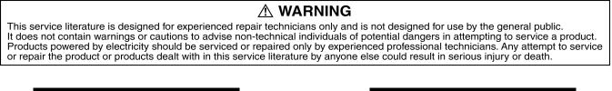
Leakage Current Cold Check
1.Unplug the AC cord and connect a jumper between the two prongs on the plug.
2.Turn on the PlasmaDisplay’s power switch.
3.Measure the resistance value, with an ohmmeter, between the jumpered AC plug and each exposed metallic cabinet part on the Plasma Display, such as screw heads, connectors, control shafts, etc. When the exposed metallic part has a return path to the chassis, the reading should be between 4 M and 20 M .
When the exposed metal does not have a return path to the chassis, the reading must be .
Leakage Current Hot Check (See Fig.1)
1.Plug the AC cord directly into the AC outlet. Do not use an isolation transformer for this check.
2.Connect a 2k , 10W resistor, in series with an exposed metallic part on the projection monitor and an earth such as a water pipe.
3.Use an AC voltmeter, with high impedance type, to measure the potential across the resistor.
4.Check each exposed metallic part, and measure the voltage at each point.
5.Reverse the AC plug in the AC outlet and repeat each of the above measurements.
6.The potential at any point should not exceed 1.0V rms. In case a measurement is outside of the limits specified, there is a possibility of a shock hazard,
- 3 -
and the projection monitor should be repaired and rechecked before it is returned to the customer.
Hot-Check Circuit
AC Voltmeter
To |
|
Water Pipe |
|
( Earth ) |
|
Instrument's |
|
|
2k |
, 10W |
Exposed
Metallic Parts
Fig. 1
Plasma Display Technology
Plasma display panel
|
|
|
|
|
|
|
CRT |
PDP |
|
|
|
|
|
|
|
Scan |
Dot Sequence |
Line Sequence |
|
|
|
|
|
|
|
|
Interlace/ |
Progressive |
|
|
|
Progressive |
|
|
|
|
|
|
|
|
Emission |
Dot Sequence |
Simultaneous |
|
|
|
|
|
|
|
Phosphor |
Electron |
Ultra Violet Lay |
|
|
Excitation |
|
|
|
|
|
|
|
|
|
Brightness |
Beam Current |
Discharge Time |
|
|
Control |
control |
control |
|
|
|
|
(Sub-Filed Drive) |
|
|
|
|
|
|
|
|
|
|
|
|
|
FIg. A |
|
|
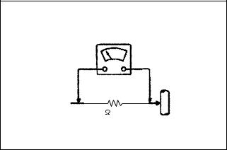
Toshiba 42 inch wide plasma display panel is developed for large screen multimedia display with space saving.
The plasma display panel use AC type Sub-field drive system with Dual scanning system.
This panel have also Asymmetric cell and Plasma AI technology.
Fig. A is the CRT and Plasma Display Panel (PDP) comparison chart.
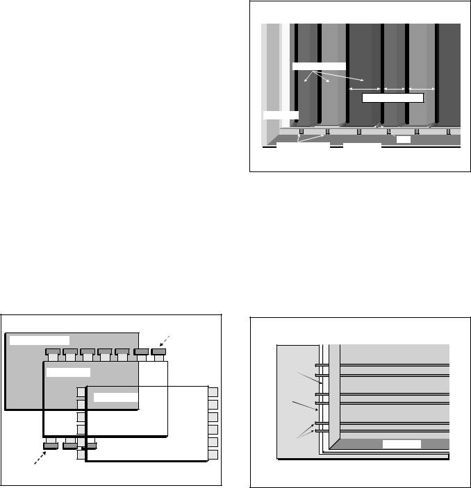
Plasma display panel structure
Data Drive Boards |
Aluminum Base |
Rear Glass |
;;;;;;;yyyyyyy |
;;yy;;;;;;;yyyyyyyFront Glass |
;;yy;;;;;;;yyyyyyy |
;;yy;;;;;;;yyyyyyy |
;;;;;;;yyyyyyy |
Data Drive Boards |
Fig. B
Plasma display panel structure.
Plasma display panel is consist of front glass, rear glass and Aluminum base.
The front glass has each 480 lines scan and sustain transparence electrodes.
The rear glass has 2556 (852 x 3) data electrodes on the inner surface. These electrodes are connected to the data drive circuit boards directly.
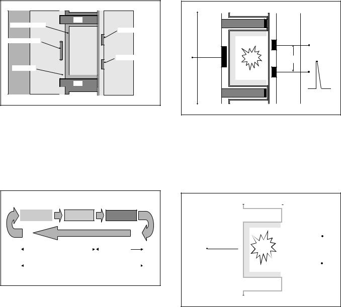
Rear Glass Structure
Color Phosphor |
|
|
Asymmetrical Cell |
Dielectrics |
|
Data Electrodes |
Rib |
Rear Glass |
|
Fig. C
On the rear glass the data electrode is mounted. The dielectric is coated on the rear glass.
Red, Green and Blue color phosphors are formed on the data electrode with the ribs. However to improve color reproduction and brightness, each color phosphors are formed different width This is called “Asymmetrical cell“ as original technology.
Front Glass Structure
Dielectrics |
|
MgO |
|
Scan & Sustain |
Front Glass |
Electrodes |
|
Fig. D
On the front glass scan and sustain transparent electrodes are mounted in pair.
The dielectrics is coated on the front grass. MgO over coat is also applied on the dielectrics.
The front and rear glasses are piled and sealed. And low presser gas are charged between two glasses.
- 4 -
Pixel Structure |
|
|
|
|
Rib |
Color Phosphor |
Scan Electrode |
|
|
|
|
Data Electrode |
Xenon |
|
|
|
+ |
|
|
Neon |
|
|
Sustain Electrode |
Dielectrics |
|
|
Aluminum |
|
Rib |
Base |
Rear Glass |
Front Glass |
Fig. E
42 inch plasma display panel has 1,226,880 pixels. Each pixels structure is shown fig. E.
Sub Field Drive system
Initialize |
Write |
Sustain |
|
Address |
|
|
|
Sustain |
||
|
Period |
|
Period |
||||
|
|
Sub Field |
|
|
|
||
|
|
|
|
|
|||
Fig. F
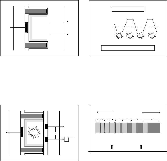
Brightness control of plasma display panel is carried out by plasma discharge time change. To control each pixel’s brightness Sub-field drive system is used.
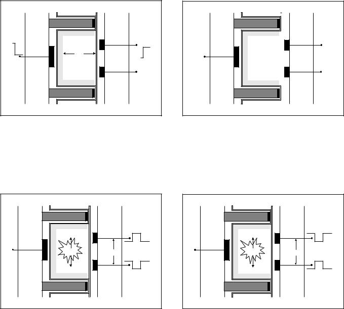
A sub-field is consist of Initialize, Write and sustain operation.
Initialization |
l |
l |
l |
VI |
+++ |
Fig. G
To clear any remaining electric charge into the pixel, trapezoid voltage is applied between the scan and sustain electrodes.
Plasma discharge is started but the discharge become small gradually.
Then any electric charge is cleared.
Write
|
|
|
|
|
|
|
|
|
|
|
|
|
|
|
|
|
|
|
|
|
|
|
|
|
|
|
|
|
|
|
|
|
|
|
|
|
|
|
|
|
|
|
|
|
|
|
|
|
|
|
|
|
|
|
|
|
|
|
|
|
|
|
|
|
|
|
|
|
|
|
|
|
|
|
|
|
|
|
|
+++++ |
|
|
|| | | | |
+++++ |
|
|
| | |
|
|
|
|
|
|
|
|
|
|
|
|
|
|
|
|||||||||||
|
|
|
|
|
|
|
|
| | | |
|
|
|
|
|
|
||||
|
|
|
|
|
|
|
|
|
|
|
|
|
|
|||||
Data Pulse |
|
|
|
|
|
|
|
|
|
|
|
|
|
|||||
|
|
|
|
|
|
|
|
|
Scan Pulse |
|||||||||
|
|
|
|
|
|
|
|
|
|
|
|
|
||||||
|
|
|
|
|
|
|
|
|
|
|
|
|
|
|
|
|
|
|
|
|
|
|
|
|
|
|
|
|
|
|
|
|
|
|
|
|
|
|
|
|
|
|
|
|
|
|
|
|
|
|
|
|
|
|
|
|
|
|
|
|
|
|
|
|
|
|
|
|
|
|
|
|
|
|
|
|
|
|
|
|
|
|
|
|
|
|
|
|
|
|
|
|
|
|
+ Ions |
|
|
|
|
|
|
|
|
|
|
|
|
|
|
|
|||
- Electrons |
|
|
|
|
|
|
|
|
|
|
|
|
|
|
|
|||
|
|
|
|
|
|
|
|
|
|
|
|
|
|
|
||||
Fig. H
Data Pulse which is positive polarity is input to data electrode and Scan pulse which is negative polarity is input to scan electrode simultaneously.
That means sum of data and scan pulses voltage is applied between two electrodes as discharge start voltage. Discharge is started into the pixel and gas is ionized.
During discharging ion is charged on the scan electrode side and electron is charged on data electrode side.
- 5 -
Wall Voltage
| |
Vw |
++++ |
| |
|
|
|
|
|
| |
|
|
| |
|
|
Fig. I
when input pulses are stopped, Ions and Electrons which are charged on the dielectric around the electrodes are remained.
This charge is called Wall Voltage (Pilot voltage). This operation is called Write.
Sustain Step 1
++++ |
+++ |
Vs + Vw |
Vs |
|
|
| |
|
| |
| |
|
|
| |
| |
|
|
| |
| |
|
Fig. J
Negative polarity’s Sustain pulse is input between sustain and scan electrodes and voltage potential between two electrodes becomes sum of Sustain pulse and wall voltage.
Then discharge start.
Sustain Step 2

 +++ | | |
Fig. K
When sustain pulse is stopped, Ions and Electrons are remained again as Wall voltage. However polarity of wall voltage is reversed.
Sustain Step 3
| |
| |
| |
| |
| |
| |
Vs + Vw |
Vs |
|
|
+++ |
+++ |
Fig. L
Positive polarity’s Sustain pulse is input between sustain and scan electrodes and discharge start again.
- 6 -
Sustain Step 4


 | | | +++
Fig. M
When sustain pulse is stopped, Ions and Electrons are remained again as Wall voltage. However polarity of wall voltage is reversed.
Sustain Step 5
+++ |
+++ |
|
Vs |
| |
| |
| |
| |
| |
| |
Fig. N
Ions and Electrons which is generated by 2nd sustain discharge are charged on the pixel wall (dielectric) around the electrodes.
Repeat Step 1 to Step 5
Sustain Cycle
Sustain Pulse
AC Drive Type Plasma Display
Fig. O
To keep discharge continuously step 1 to 5 operation will be repeated.
As the result sustain pulse is alternated. Therefore we call this drive system AC Drive type.
If sustain operation is repeated longer, brightness level of the pixel is increased. Therefore depend on sustain discharge time brightness of pixel is controlled.
Sub-Field drive
|
|
|
|
|
|
1 TV Field |
|
|
|
|
|
|
|
|
= |
|
|
|
|
|
|
|
|
8 Sub Fields |
|
|
1st |
2nd 3nd |
4th |
5th |
6th |
7th |
8th |
||
|
1 |
2 |
4 |
8 |
16 |
32 |
64 |
128 |
|
|
|
|
|
Address Period |
|
Sustain Period |
|
Fig. P
Sub-Field drive is PDP unique system.
While one TV field period, 8 bits digital video signal component is reproduced by 8 sub-fields operation.
Each Sub-Field’s address period are all same.(Consist of one initialization and 480 scanning operation.)
But Sustain period of each Sub-Field are different. 1st Sub-Field (SF) reproduce only 1 step brightness. 2nd SF reproduce 2 steps brightness.
Each sub-field’s sustain period are increased gradually. However total 256 brightness difference can be reproduced on the screen.
- 7 -
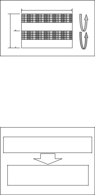
Dual Scan
852
480 240 240
Fig. Q
The sustain period of sub-field drive system. Therefore brightness peak is limited. Because 480 horizontal lines scanning is carried out during address period.
Dual scan system can reduce scanning time from 480 to 240 in the address period.
Then spaced time by dual scanning can be used for sustain operation.
As the result Brightness peak level can be increased.
Plasma AI (Adaptive brightness Intensifier)
•Increase Peak Brightness in Dark scenes •Reduce Motion Picture Disturbance •Keep Reasonable Power Consumption
Multi Split Sub-Field Drive System
1. Linear coding Sub-Field
+
2. Variable Sub-Field
Fig. R
Plasma AI control sub-field drive operation which is called Multi-Split Sub-Field drive control system is used.
Depend on the picture contents (APL: Average Picture Level) number of sub-field are changed from 10 to 12. (Variable Sub-field)
Sustain time format of each sub-field are also rearranged from binary format to linear cording sustain time. (Linear coding sub-field)
Plasma AI select the best display condition for Plasma display panel to display natural and crisp picture.
- 8 -

Service Hint
Remove the Back Cover |
screw(1) |
Back Cover |
|
(30mm) |
|
|
|
Stand the Unit used for Optional Accessory
screw(4)
(20mm)
Optional Accessory |
|
|
|
|
|
|
screw(2) |
(Pedestal) |
|
|
|
|
|
|
|
|
|
|
|
|
screw(3) |
(17mm) |
|
|
|
|
|
|
|
||
|
|
|
|
|
|
(8mm) |
|
|
|
|
|
|
|
Remove: 6 screws (1) |
|
|
|
C1 |
C2 |
|
SS2 |
10 screws (2) |
|
|
|
|
|
|
|
9 screws (3) |
|
SU |
|
D |
|
|
|
4 screws (4) |
|
|
|
|
|
|
|
||
|
|
|
|
|
|
|
|
|
|
P8 |
|
|
P7 |
|
|
|
|
DS |
|
|
|
|
|
|
SC |
|
P1 |
|
SS |
|
|
|
|
HG |
|
P5 |
P3 |
|
|
|
|
|
P6 |
|
|
||
|
|
|
|
|
|
|
|
SD |
|
|
|
|
|
Service Position |
|
|
|
|
|
|
|
|
|
|
H3 |
H2 |
|
|
|
|
|
|
|
|
C3 |
SS3 |
|
|
|
|
|
F |
|
|
|
||
|
|
C4 |
|
|
|
|
|
S2 |
|
|
V1 |
|
S1 |
|
|
(Front) |
|
|
(Front) |
|
(Front) |
|
|
Board name |
Function |
Board name |
Function |
|
|
|
|
|
|
|
|
DS module |
I/P Converter |
V1 board |
Front Switch |
|
|
|
|
HG board |
Interface |
S1 board |
Power Switch & Remote Receiver |
|
|
|
|
D board |
Digital process & Control |
S2 board |
Factory use |
|
|
|
|
P1 board |
Power supply |
P3 board |
Sustain voltage control |
|
|
|
|
SC board |
Scan drive |
P5 board |
Processing voltage control |
|
|
|
|
SS board |
Sustain Drive |
P6 board |
Primary voltage control |
|
|
|
|
C1 board |
Data drive (Upper Left) |
P7 board |
Sustain voltage protection |
|
|
|
|
C2 board |
Data drive (Upper Right) |
P8 board |
Processing voltage protection |
|
|
|
|
C3 board |
Data drive (Lower Right) |
H2 board |
PC input terminal |
|
|
|
|
C4 board |
Data drive (Lower Left) |
F board |
Line filter |
|
|
|
|
SU board |
Scan out (Upper) |
H3 board |
Speaker terminal |
|
|
|
|
SD board |
Scan out (Lower) |
SS2 board |
Sustain connection (Upper) |
|
|
|
|
|
|
SS3 board |
Sustain connection (Lower) |
|
|
|
|
- 9 -
Adjustment Procedure
Item / Preparation
+B Set-Up
1.Confirm the main voltage set switch
is set to 110V.(U model) or 230V (E model)
Adjustments
230 V 
 110 V
110 V
P6 board
Note: 230V covers input AC voltage from 200V till 265V, and 110V covers from 90V till 130V.
2.Input a Grey scale signal.
3.Set the picture controls: -
Picture mode |
Normal |
White balance |
Normal |
Driver Set-Up
4.Input an APL 100% white signal.
5.Set the picture controls: -
Picture mode |
Normal |
White balance |
Normal |
Adjust and confirm indicated test point for the specified voltage
Test Point |
Voltage |
Volume |
Name |
|
|
|
|
|
|
|
|
P4 pin 1 (Hot) |
400 V ± 1 V |
R548 |
PFC |
|
|
|
|
Confirmation (Cold) |
|
|
|
|
|
|
|
P1 pin 10 |
15 V ± 0.5 V |
|
+15 V |
|
|
|
|
P5 pin 1 |
13 V ± 0.5 V |
|
+13 V |
|
|
|
|
P6 pin 1 |
13 V ± 0.5 V |
|
Audio 13 V |
|
|
|
|
P6 pin 3 |
-13 V ± 0.5 V |
|
Audio -13 V |
|
|
|
|
P5 pin 5 |
5 V ± 0.5 V |
|
+5 V |
|
|
|
|
P5 pin 8 |
3.4 V ± 0.5 V |
|
+3.3 V |
|
|
|
|
P7 pin 1 |
14 V ± 1 V |
|
STB 14V |
|
|
|
|
P7 pin 6 |
5 V ± 0.5 V |
|
STB 5 V |
|
|
|
|
Adjust driver section voltages referring panel data on the panel data label.
Test point |
Voltage |
Volume |
Name |
|
|
|
|
|
|
|
|
TPDA1(C1) |
75 V ± 0.5 V |
R528(P1) |
VDA |
|
|
|
|
TPVSUS(SS) |
VSUS ± 1 V |
R639(P3) |
VSUS |
|
|
|
|
TPVSET(SC) |
VSET ± 1 V |
R6587(SC) |
VSET |
|
|
|
|
TPVSCN(SC) |
80 V ± 0.5 V |
R6597(SC) |
VSCN |
|
|
|
|
TPVE(SS) |
VE ± 0.5 V |
R494(P1) |
VE |
|
|
|
|
- 10 -
 Loading...