UC1902
UC2902
UC3902
PRELIMINARY
SLUS232 - FEBRUARY 1999
FEATURES
• 2.7V to 20V Operation
• 8-Pin Package
• Requires Minimum Number of
External Components
• Compatible with Existing Power
Supply Designs Incorporating Remote
Output Voltage Sensing
• Differential Share Bus
• Precision Current Sense Amplifier with
Gain of 40
• UVLO (Undervoltage Lockout)
Circuitry
• User Programmable Share Loop
Compensation
Load Share Controller
1
3
2
4
8
6
7
5
+
–
R
40R
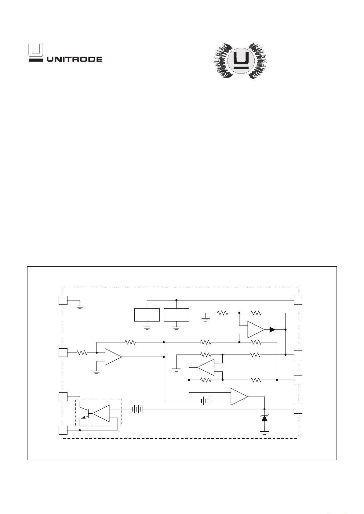
LOAD SHARECONTROLLER
+
–
ADJ AMPLIFIER
BIAS UVLO
+
–
+
–
+
–
SHARE SENSE AMPLIFIER
SHARE DRIVE AMPLIFIER
2.3V
35mV
+
0.6V
+
CURRENT SENSE
AMPLIFIER
ERROR AMPLIFIER
GND
SENSE
ADJ
ADJR
VCC
SHARE+
SHARE–
COMP
BLOCK DIAGRAM
UDG-99042
DESCRIPTION
The UC3902 load share controller is an 8-pin device that balances the current drawn from independent, paralleled power supplies. Load sharing is
accomplished by adjusting each supply’s output current to a level proportional to the voltage on a share bus.
The master power supply, which is automatically designated as the supply
that regulates to the highest voltage, drives the share bus with a voltage
proportional to its output current. The UC3902 trims the output voltage of
the other paralleled supplies so that they each support their share of the
load current. Typically, each supply is designed for the same current level
although that is not necessary for use with the UC3902. By appropriately
scaling the current sense resistor, supplies with different output current capability can be paralleled with each supply providing the same percentage
of their output current capability for a particular load.
A differential line is used for the share bus to maximize noise immunity and
accommodate different voltage drops in each power converter’s ground return line. Trimming of each converter’s output voltage is accomplished by
injecting a small current into the output voltage sense line, which requires a
small resistance (typically 20Ω – 100Ω) to be inserted.

2
UC1902
UC2902
UC3902
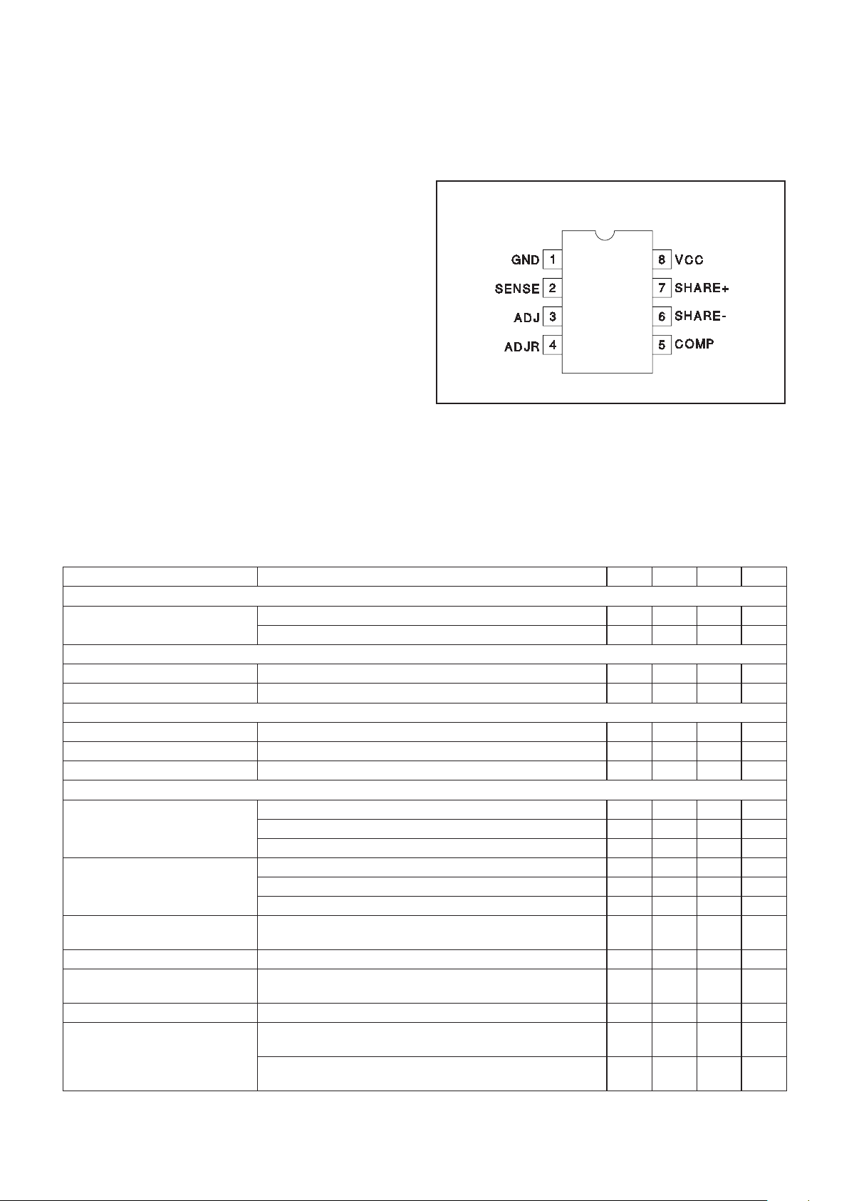
CONNECTION DIAGRAM
DIL-8, SOIC-8 (Top View)
N, J and D Package
ELECTRICAL CHARACTERISTICS:
Unless otherwise specified, TA= –55°C to +125°C for UC1902, –40°C to+85°C for
UC2902, 0°C to 70°C for UC3902, VCC = 5V, R
ADJR
= 1kΩ, V
ADJ
= 5V, COMP = 5nF capacitor to GND, V
SHARE
–
= 0V, TA= TJ.
PARAMETERS TEST CONDITIONS MIN TYP MAX UNIT
Power Supply
Supply Current SHARE+ = 1V, SENSE = 0V 4 6 mA
VCC = 20V 6 10 mA
Undervoltage Lockout
Startup Voltage SHARE+ = 0.2V, SENSE = 0V, COMP = 1V 2.3 2.5 2.7 V
Hysteresis SHARE+ = 0.2V, SENSE = 0V, COMP = 1V 60 100 140 mV
Current Sense Amplifier
Input Offset Voltage 0.1V ≤ SHARE+ ≤ 1.1V –2.5 –0.5 1.5 mV
Gain SENSE to SHARE 0.1V ≤ SHARE+ ≤ 1.1V –41 –40 -39 V/V
Input Resistance 0.6 1 1.5 kΩ
Share Drive Amplifier
SHARE+ High VCC = 2.5V, SENSE = –50mV, I
SHARE+ = –1mA 1.2 1.4 V
VCC = 12V, SENSE = –250mV, I
SHARE+ = –1mA 9.6 10 10.4 V
VCC = 20V, SENSE = –250mV, I
SHARE+ = –1mA 9.6 10 10.4 V
SHARE+ Low VCC = 2.5V, SENSE = +10mV, I
SHARE+ = –1mA 20 50 mV
VCC = 12V, SENSE = +10mV, I
SHARE+ = –1mA 20 50 mV
VCC = 20V, SENSE = +10mV, I
SHARE+ = –1mA 20 50 mV
SHARE+ Output Voltage Measures SHARE+, SENSE = 0mV, R
SHARE+ = 200Ω resistor
SHARE+ to GND
20 40 mV
CMRR 0 ≤ SHARE– ≤ 1V , SENSE used as input to amplifier 50 90 dB
Load Regulation Load on SHARE+, –1mA ≤ I
LOAD ≤ –20mA, SENSE =
–25mV
020mV
Short Circuit Current SHARE+ = 0V, SENSE = –25mV –85 –50 –20 mA
Slew Rate SENSE = +10mV to –90mV Step, 200Ω resistor SHARE+ to
GND
0.16 0.27 0.37 V/µs
SENSE = –90mV to +10mV Step, 200Ω resistor SHARE+ to
GND
0.12 0.24 0.34 V/µs
Supply Voltage (ADJ and VCC) . . . . . . . . . . . . . . –0.3V to 20V
SENSE Voltage . . . . . . . . . . . . . . . . . . . . . . . . . . . . –5V to +5V
ADJR, COMP Voltage. . . . . . . . . . . . . . . . . . . . . . –0.3V to +4V
SHARE–, SHARE+ Voltages . . . . . . . . . . . . . . . . –0.3V to 10V
SHARE+ Current . . . . . . . . . . . . . . . . . . . . . –100mA to +10mA
ADJ Current . . . . . . . . . . . . . . . . . . . . . . . . . . . –1mA to +30mA
Storage Temperature . . . . . . . . . . . . . . . . . . . –65°C to +150°C
Junction Temperature. . . . . . . . . . . . . . . . . . . –55°C to +150°C
Lead Temperature (Soldering, 10sec.) . . . . . . . . . . . . . +300°C
All voltages are with respect to pin 1. Currents are positive into,
negative out of the specified terminal. Consult Packaging Section of the Databook for thermal limitations and considerations
of packages.
ABSOLUTE MAXIMUM RATINGS
 Loading...