

UC1902
UC2902
UC3902
PRELIMINARY
SLUS232 - FEBRUARY 1999
FEATURES
• 2.7V to 20V Operation
• 8-Pin Package
• Requires Minimum Number of
External Components
• Compatible with Existing Power
Supply Designs Incorporating Remote
Output Voltage Sensing
• Differential Share Bus
• Precision Current Sense Amplifier with
Gain of 40
• UVLO (Undervoltage Lockout)
Circuitry
• User Programmable Share Loop
Compensation
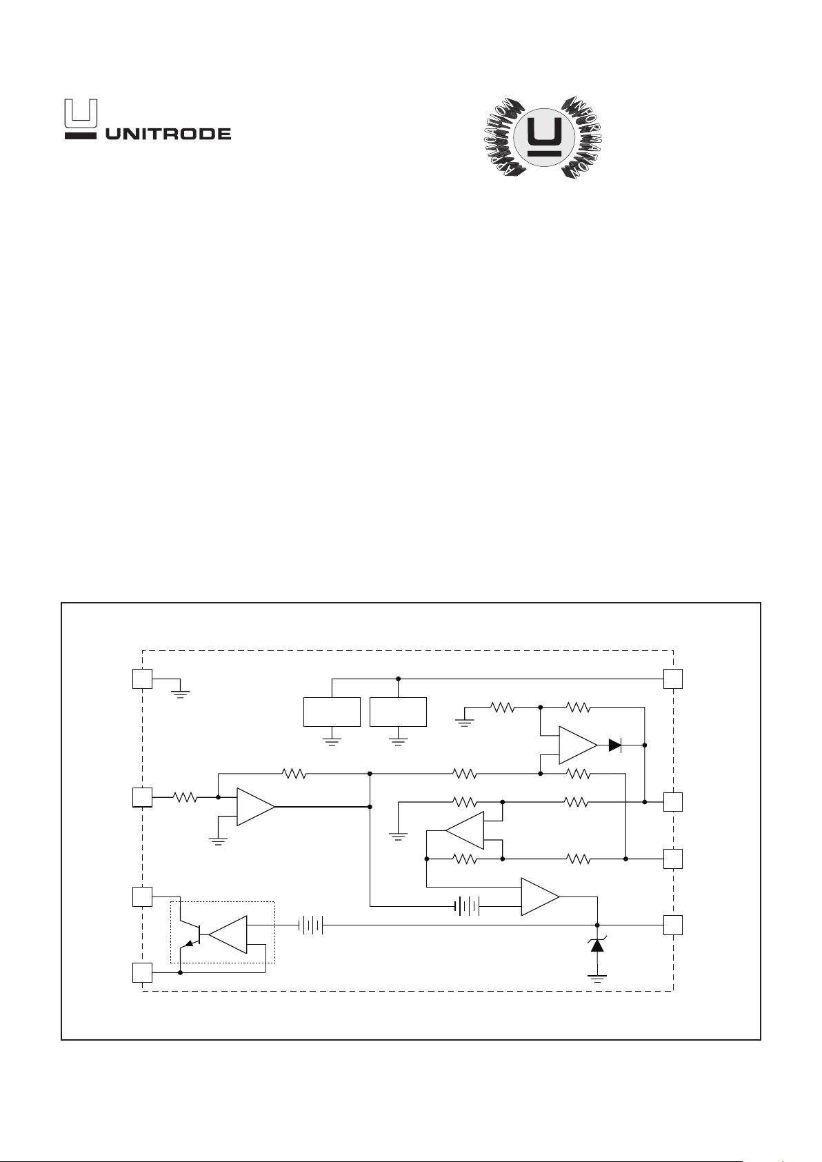
Load Share Controller
1
3
2
4
8
6
7
5
+
–
R
40R
LOAD SHARECONTROLLER
+
–
ADJ AMPLIFIER
BIAS UVLO
+
–
+
–
+
–
SHARE SENSE AMPLIFIER
SHARE DRIVE AMPLIFIER
2.3V
35mV
+
0.6V
+
CURRENT SENSE
AMPLIFIER
ERROR AMPLIFIER
GND
SENSE
ADJ
ADJR
VCC
SHARE+
SHARE–
COMP
BLOCK DIAGRAM
UDG-99042
DESCRIPTION
The UC3902 load share controller is an 8-pin device that balances the current drawn from independent, paralleled power supplies. Load sharing is
accomplished by adjusting each supply’s output current to a level proportional to the voltage on a share bus.
The master power supply, which is automatically designated as the supply
that regulates to the highest voltage, drives the share bus with a voltage
proportional to its output current. The UC3902 trims the output voltage of
the other paralleled supplies so that they each support their share of the
load current. Typically, each supply is designed for the same current level
although that is not necessary for use with the UC3902. By appropriately
scaling the current sense resistor, supplies with different output current capability can be paralleled with each supply providing the same percentage
of their output current capability for a particular load.
A differential line is used for the share bus to maximize noise immunity and
accommodate different voltage drops in each power converter’s ground return line. Trimming of each converter’s output voltage is accomplished by
injecting a small current into the output voltage sense line, which requires a
small resistance (typically 20Ω – 100Ω) to be inserted.
2
UC1902
UC2902
UC3902
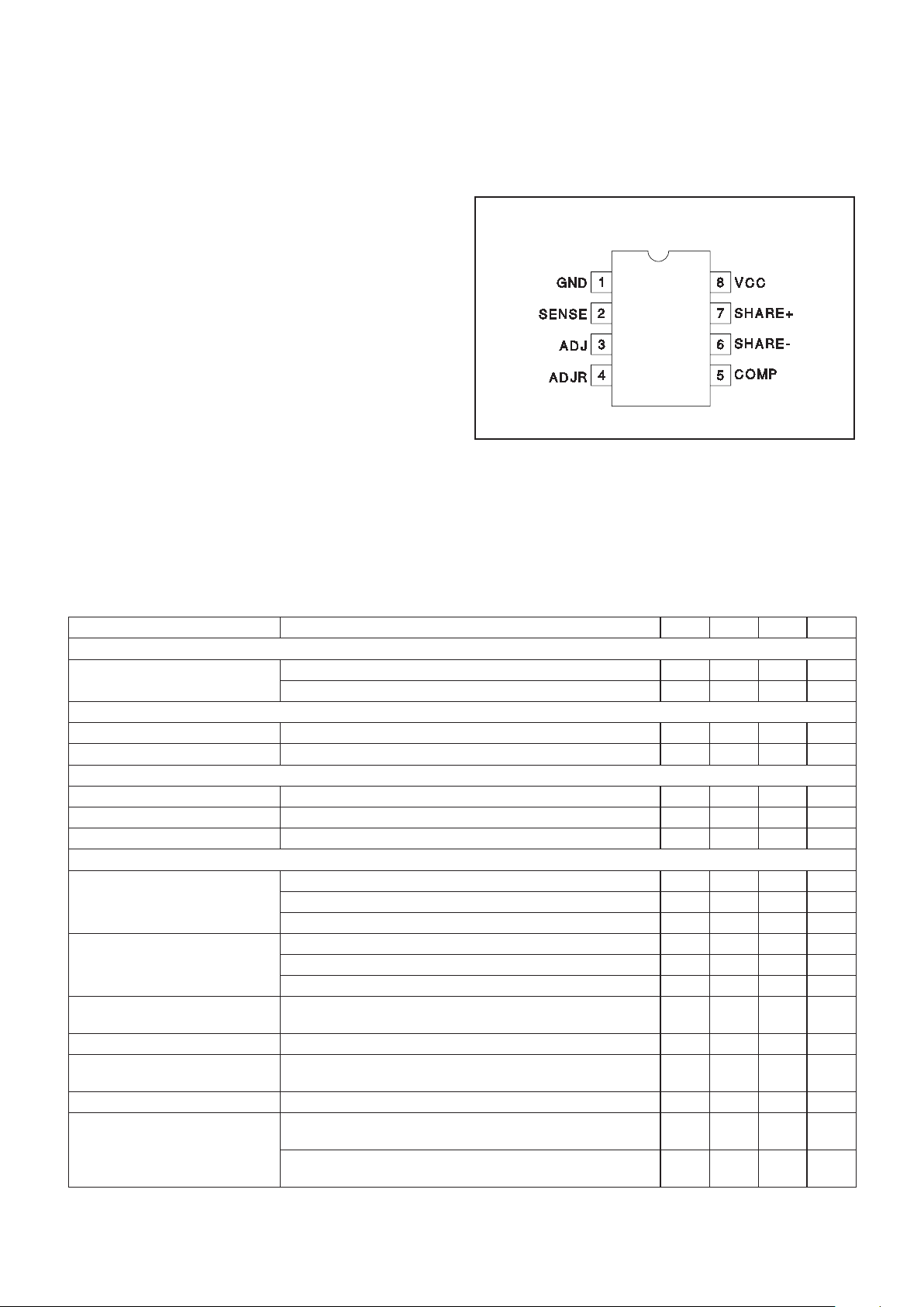
CONNECTION DIAGRAM
DIL-8, SOIC-8 (Top View)
N, J and D Package
ELECTRICAL CHARACTERISTICS:
Unless otherwise specified, TA= –55°C to +125°C for UC1902, –40°C to+85°C for
UC2902, 0°C to 70°C for UC3902, VCC = 5V, R
ADJR
= 1kΩ, V
ADJ
= 5V, COMP = 5nF capacitor to GND, V
SHARE
–
= 0V, TA= TJ.
PARAMETERS TEST CONDITIONS MIN TYP MAX UNIT
Power Supply
Supply Current SHARE+ = 1V, SENSE = 0V 4 6 mA
VCC = 20V 6 10 mA
Undervoltage Lockout
Startup Voltage SHARE+ = 0.2V, SENSE = 0V, COMP = 1V 2.3 2.5 2.7 V
Hysteresis SHARE+ = 0.2V, SENSE = 0V, COMP = 1V 60 100 140 mV
Current Sense Amplifier
Input Offset Voltage 0.1V ≤ SHARE+ ≤ 1.1V –2.5 –0.5 1.5 mV
Gain SENSE to SHARE 0.1V ≤ SHARE+ ≤ 1.1V –41 –40 -39 V/V
Input Resistance 0.6 1 1.5 kΩ
Share Drive Amplifier
SHARE+ High VCC = 2.5V, SENSE = –50mV, I
SHARE+ = –1mA 1.2 1.4 V
VCC = 12V, SENSE = –250mV, I
SHARE+ = –1mA 9.6 10 10.4 V
VCC = 20V, SENSE = –250mV, I
SHARE+ = –1mA 9.6 10 10.4 V
SHARE+ Low VCC = 2.5V, SENSE = +10mV, I
SHARE+ = –1mA 20 50 mV
VCC = 12V, SENSE = +10mV, I
SHARE+ = –1mA 20 50 mV
VCC = 20V, SENSE = +10mV, I
SHARE+ = –1mA 20 50 mV
SHARE+ Output Voltage Measures SHARE+, SENSE = 0mV, R
SHARE+ = 200Ω resistor
SHARE+ to GND
20 40 mV
CMRR 0 ≤ SHARE– ≤ 1V , SENSE used as input to amplifier 50 90 dB
Load Regulation Load on SHARE+, –1mA ≤ I
LOAD ≤ –20mA, SENSE =
–25mV
020mV
Short Circuit Current SHARE+ = 0V, SENSE = –25mV –85 –50 –20 mA
Slew Rate SENSE = +10mV to –90mV Step, 200Ω resistor SHARE+ to
GND
0.16 0.27 0.37 V/µs
SENSE = –90mV to +10mV Step, 200Ω resistor SHARE+ to
GND
0.12 0.24 0.34 V/µs
Supply Voltage (ADJ and VCC) . . . . . . . . . . . . . . –0.3V to 20V
SENSE Voltage . . . . . . . . . . . . . . . . . . . . . . . . . . . . –5V to +5V
ADJR, COMP Voltage. . . . . . . . . . . . . . . . . . . . . . –0.3V to +4V
SHARE–, SHARE+ Voltages . . . . . . . . . . . . . . . . –0.3V to 10V
SHARE+ Current . . . . . . . . . . . . . . . . . . . . . –100mA to +10mA
ADJ Current . . . . . . . . . . . . . . . . . . . . . . . . . . . –1mA to +30mA
Storage Temperature . . . . . . . . . . . . . . . . . . . –65°C to +150°C
Junction Temperature. . . . . . . . . . . . . . . . . . . –55°C to +150°C
Lead Temperature (Soldering, 10sec.) . . . . . . . . . . . . . +300°C
All voltages are with respect to pin 1. Currents are positive into,
negative out of the specified terminal. Consult Packaging Section of the Databook for thermal limitations and considerations
of packages.
ABSOLUTE MAXIMUM RATINGS

3
UC1902
UC2902
UC3902
ELECTRICAL CHARACTERISTICS: Unless otherwise specified, T
A
= –55°C to +125°C for UC1902, –40°C to+85°C for
UC2902, 0°C to 70°C for UC3902, VCC = 5V, R
ADJR
= 1kΩ, V
ADJ
= 5V, COMP = 5nF capacitor to GND, V
SHARE
–
= 0V, TA= TJ.
PARAMETERS TEST CONDITIONS MIN TYP MAX UNIT
Share Sense Amplifier
Input Impedance SHARE+ = 1V, SHARE– = 1V, SENSE = +10mV 10 15 kΩ
200Ω resistor SHARE+ to GND, SHARE– = 1V, SENSE =
+10mV
15 17 kΩ
Threshold SENSE = 0V 41 70 100 mV
CMRR SHARE 0 ≤ SHARE– ≤ 1V, SENSE = –2.5mV 50 60 dB
AVOL from SHARE+ to ADJR SENSE = –2.5mV, 5nF capacitor COMP to GND, 1k resistor
ADJR to GND
50 68 dB
SENSE = –2.5mV, 5nF capacitor COMP to GND, 150Ω
resistor ADJR to GND
50 66 dB
Slew Rate SHARE+ = Step of 0mV to 300mV through a 200Ω resistor,
R
COMP = 500Ω resistor to 1.5V, SENSE = 10mV
0.4 0.7 1 V/µs
Error Amplifier Section
Transconductance, SHARE+
to COMP
200Ω resistor SHARE+ to GND 3.2 4.5 5.5 mS
IOH COMP = 1.5V, SHARE+ ≥ +300mV, SENSE = +10mV –400 –325 –230 µA
IOL 200Ω resistor SHARE+ to GND, COMP = 1.5V, SENSE =
+10mV
100 150 200 µA
Input Offset Voltage 15 35 65 mV
∆ VIO/∆ V
SENSE 1k Resistor, ADJR to GND, –2.5mV < SENSE < –25mV –6 0 6 mV/V
ADJ Amplifier
ADJR Low Voltage SENSE = +10mV, 200Ω resistor SHARE+ to GND –1 0 1 mV
ADJR High Voltage SENSE = +10mV, SHARE+ = 1V 1.4 1.8 2.1 V
Current Gain ADJR to ADJ ADJR Current = –0.5mA, ADJ = 2.5V, SENSE = +10mV,
SHARE+ = 1V
0.96 0.99 1 A/A
ADJR Current = –0.5mA, ADJ = 20V, SENSE = +10mV,
SHARE+ = 1V
0.96 0.99 1 A/A
ADJR Current = –10mA, ADJ = 2.5V, SENSE = +10mV,
SHARE+ = 1V
0.96 0.99 1 A/A
ADJR Current = –10mA, ADJ = 20V, SENSE = +10mV,
SHARE+ = 1V
0.96 0.99 1 A/A
ADJ: Current output of adjust amplifier circuit (NPN
collector).
ADJR: Current adjust amplifier range set (NPN emitter).
COMP: Output of error amplifier, input of adjust amplifier.
This is where the compensation capacitor is connected.
GND: Local power supply return and signal ground.
SENSE: Inverting input of current sense amplifier.
SHARE+: Positive input from share bus or drive to share
bus.
SHARE-: Reference for SHARE+.
VCC: Local power supply (positive).
PIN DESCRIPTIONS

4
UC1902
UC2902
UC3902
Figure 1. Typical application.
APPLICATION INFORMATION
UDG-96200

5
UC1902
UC2902
UC3902
UNITRODE CORPORATION
7 CONTINENTAL BLVD.• MERRIMACK, NH 03054
TEL. (603) 424-2410 FAX (603) 424-3460
The values of five passive components must be determined to configure the UC3902 load share controller.
The output and return lines of each converter are connected together at the load, with current sense resistor
R
SENSE
inserted in each negative return line. Another re-
sistor, R
ADJ,
is also inserted in each positive remote
sense line. The differential share bus terminals (SHARE+
and SHARE–) of each UC3902 are connected together
respectively, and the SHARE– node is also connected to
the system ground. A typical application is illustrated in
Figure 1.
The load share controller design can be executed by following the next few steps:
Step 1.
()
()
R
V
AI
SENSE
SHARE
CSA O
=
•
max
max
where A
CSA
is 40, the gain of the current sense amplifier.
At full load, the voltage drop across the R
SENSE
resistor
is I
O
(max) • R
SENSE
. Taking into account the gain of the
current sense amplifier, the voltage at full load on the
current share bus,
() ()
VAIR
SHARE CSA O SENSE
max max=• •
.
This voltage must stay 1.5V below V
CC
or below 10V
whichever is smaller. V
SHARE
represents an upper limit
but the designer should select the full scale share bus
voltage keeping in mind that every volt on the load share
bus will increase the master controller’s supply current by
approximately 100mA times the number of slave units
connected parallel.
Step 2.
()
()
R
V
I
G
ADJ
ADJ
=
max
max
Care must be taken to ensure that I
ADJ
(max)
is low
enough to ensure that both the drive current and power
dissipation are within the UC3902’s capability. For most
applications, an I
ADJ
(max) current between 5mA and
10mA is acceptable. In a typical application, a 360Ω R
G
resistor from the ADJR pin to ground sets I
ADJ
(max) to
approximately 5mA.
Step 3.
()()
()
RADJ
VIR
I
O O SENSE
ADJ
=
•∆ max – max
max
R
ADJ
must be low enough to not affect the normal operation of the converter’s voltage feedback loop. Typical
R
ADJ
values are in the 20Ω to100Ω range depending on
V
O
, ∆VO(max) and the selected I
ADJ
(max) value.
Step 4.
()
C
G
fCRR
R
R
AAfC
C
MADJ
G
SENSE
LOAD
CSA PWR
=
••
•• ••
2
π
The share loop compensation capacitor, CCis calculated
to produce the desired share loop unity gain crossover
frequency, fC. The share loop error amplifier’s
transconductance, G
M
is nominally 4.5ms. The values of
the resistors are already known. Typically, fC will be set
at least an order of magnitude below the converter’s
closed loop bandwidth. The load share circuit is primarily
intended to compensate for each converter’s initial output
voltage tolerance and temperature drift, not differences in
their transient response. The term A
PWR
(fC) is the gain
of the power supply measured at the desired share loop
crossover frequency, fC. This gain can be measured by
injecting the measurement signal between the positive
output and the positive sense terminal of the power supply.
Step 5.
R
fC C
C
C
=
•• •
1
2
π
A resistor in series with CC is required to boost the phase
margin of the load share loop. The zero is placed at the
load share loop crossover frequency, f
C.
When the system is powered up, the converter with the
highest output voltage will tend to source the most current and take control of the share bus.The other converters will increase their output voltages until their output
currents are proportional to the share bus voltage minus
50mV. The converter which in functioning as the master
may change due to warmup drift and differences in load
and line transient response of each converter.
ADDITIONAL INFORMATION
Please refer to the following Unitrode topic for additional
application information.
[1] Application Note U-163,
The UC3902 Load Share
Controller and Its Performance in Distributed Power Systems
by Laszlo Balogh
.
APPLICATION INFORMATION (cont.)

IMPORTANT NOTICE
T exas Instruments and its subsidiaries (TI) reserve the right to make changes to their products or to discontinue
any product or service without notice, and advise customers to obtain the latest version of relevant information
to verify, before placing orders, that information being relied on is current and complete. All products are sold
subject to the terms and conditions of sale supplied at the time of order acknowledgement, including those
pertaining to warranty, patent infringement, and limitation of liability.
TI warrants performance of its semiconductor products to the specifications applicable at the time of sale in
accordance with TI’s standard warranty. Testing and other quality control techniques are utilized to the extent
TI deems necessary to support this warranty. Specific testing of all parameters of each device is not necessarily
performed, except those mandated by government requirements.
CERT AIN APPLICATIONS USING SEMICONDUCTOR PRODUCTS MA Y INVOLVE POTENTIAL RISKS OF
DEATH, PERSONAL INJURY, OR SEVERE PROPERTY OR ENVIRONMENTAL DAMAGE (“CRITICAL
APPLICATIONS”). TI SEMICONDUCTOR PRODUCTS ARE NOT DESIGNED, AUTHORIZED, OR
WARRANTED TO BE SUITABLE FOR USE IN LIFE-SUPPORT DEVICES OR SYSTEMS OR OTHER
CRITICAL APPLICATIONS. INCLUSION OF TI PRODUCTS IN SUCH APPLICA TIONS IS UNDERSTOOD T O
BE FULLY AT THE CUSTOMER’S RISK.
In order to minimize risks associated with the customer’s applications, adequate design and operating
safeguards must be provided by the customer to minimize inherent or procedural hazards.
TI assumes no liability for applications assistance or customer product design. TI does not warrant or represent
that any license, either express or implied, is granted under any patent right, copyright, mask work right, or other
intellectual property right of TI covering or relating to any combination, machine, or process in which such
semiconductor products or services might be or are used. TI’s publication of information regarding any third
party’s products or services does not constitute TI’s approval, warranty or endorsement thereof.
Copyright 1999, Texas Instruments Incorporated
 Loading...