

Sony HCDV-3900 Service manual
HCD-V3900/V5900
SERVICE MANUAL
• This set is the tuner, deck,Video CD and
amplifier section in LBT-V3900/V5900.
Manufactured under license from Dolby Laboratories
Licensing Corporation.
“DOLBY” and the double-D symbol a are trademarks
of Dolby Laboratories Licensing Corporation.
Photo : HCD-V5900
CD CD Mechanism Type CDM37L-5BD21AL
Section Base Unit Name BU-5BD21AL
Tape deck Model Name Using Similar Mechanism HCD-V4800
Section T ape Transport Mechanism T ype TCM-220WR2
E Model
Model Name Using Similar Mechanism HCD-V4800
Optical Pick-up Name KSS-213D/Q-NP
Amplifier section
(HCD-V3900)
The following measured at AC 120/240 V, 50 Hz
DIN power output (Rated)
100 + 100 watts
(6 ohms at 1 kHz, DIN)
Continuous RMS power output (Reference)
120 + 120 watts
(6 ohms at 1 kHz, 10 % THD)
The following measured at AC 220 V, 50 Hz
DIN power output (Rated)
90 + 90 watts
(6 ohms at 1 kHz, DIN)
Continuous RMS power output (Reference)
105 + 105 watts
(6 ohms at 1 kHz, 10 % THD)
Peak music power output (Reference)
1,500 watts
(HCD-V5900)
The following measured at AC 120/240 V, 50 Hz
DIN power output (Rated)
120 + 120 watts
(6 ohms at 1 kHz, DIN)
Continuous RMS power output (Reference)
140 + 140 watts
(6 ohms at 1 kHz, 10 % THD)
The following measured at AC 220 V, 50 Hz
DIN power output (Rated)
110 + 110 watts
(6 ohms at 1 kHz, DIN)
SPECIFICATIONS
Continuous RMS power output (Reference)
130 + 130 watts
(6 ohms at 1 kHz, 10 % THD)
Peak music power output (Reference)
2,000 watts
Inputs
PHONO IN (phono jacks):
sensitivity 3 mV,
impedance 47 kilohms
VIDEO (AUDIO) IN (phono jacks):
sensitivity 250 mV,
impedance 47 kilohms
MIX MIC (phono jack):
sensitivity 1 mV,
impedance 10 kilohms
Outputs
VIDEO (AUDIO) OUT (phono jacks):
voltage 250 mV, impedance 1 kilohm
VIDEO (phono jack):
max. output level 1 Vp-p, unbalanced,
Sync negative, load impedance 75 ohms
S-VIDEO (4-pin/mini-DIN jack):
Y: 1 Vp-p, unbalanced, Sync negative
C: 0.286 Vp-p, load impedance 75 ohms
PHONES (stereo phone jack):
accepts headphones of 8 ohms or more
COMPACT HI-FI STEREO SYSTEM
SPEAKER:
accepts impedance of 6 to 16 ohms
Video CD/CD player section
System Compact disc digital audio and video
system
Laser Semiconductor laser (= 780 nm)
Emission
duration: continuous
Laser output
Max. 44.6 µW*
* This output is the value measured at a
distance of 200 mm from the objective
lens surface on the Optical Pick-up Block
with 7 mm aperture.
Wavelength
780 – 790 nm
Frequency response
2 Hz – 20 kHz (±0.5 dB)
Signal-to-noise ratio
More than 90 dB
Dynamic range
More than 90 dB
Video Color system format:
NTSC, PAL
— Continued on next page —
MICROFILM

Tape player section
Recording system
4-track 2-channel stereo
Frequency response (DOLBY NR OFF)
60 – 13,000 Hz (±3 dB), using a Sony TYPE I cassette
60 – 14,000 Hz (±3 dB), using a Sony TYPE II cassette
Tuner section
FM stereo, FM/AM superheterodyne tuner
FM tuner section
Tuning range
87.5 – 108.0 MHz (50 kHz step)
Antenna
FM wire antenna
Antenna terminals
75 ohm unbalanced
Intermediate frequency
10.7 MHz
AM tuner section
Tuning range
531 – 1,602 MHz (with the tuning interval set at 9 kHz)
530 – 1,710 MHz (with the tuning interval set at 10 kHz)
Antenna
AM loop antenna, External antenna terminals
Intermediate frequency
450 kHz
SAFETY-RELATED COMPONENT WARNING!!
COMPONENTS IDENTIFIED BY MARK ! OR DO TTED LINE WITH
MARK ! ON THE SCHEMATIC DIAGRAMS AND IN THE PARTS
LIST ARE CRITICAL TO SAFE OPERATION. REPLACE THESE
COMPONENTS WITH SONY PARTS WHOSE PART NUMBERS
APPEAR AS SHOWN IN THIS MANUAL OR IN SUPPLEMENTS
PUBLISHED BY SONY.
CAUTION
Use of controls or adjustments or performance of procedures
other than those specified herein may result in hazardous radiation
exposure.
This appliance is classified as a CLASS 1 LASER product. The
CLASS 1 LASER PRODUCT MARKING is located on the rear
exterior.
General
Power requirements 110 – 120 V or 220 – 240 V AC, 50/60 Hz
adjustable with voltage selector
Power consumption (HCD-V3900) 245 watts
(HCD-V5900) 255 watts
Dimensions (w/h/d) Approx. 355 × 425 × 435 mm incl.
projecting parts and controls
Mass (HCD-V3900) Approx. 16.3 kg
(HCD-V5900) Approx. 16.8 kg
Supplied accessories AM loop antenna (1)
Remote (1)
RM-SV808S (LBT-V3900)
RM-SV4800S (LBT-V5900)
Size AA batteries (2)
FM wire antenna (1)
Speaker cords (2)
Video cable (1)
Design and specifications are subject to change without notice.
Laser component in this product is capable
of emitting radiation exceeding the limit for
Class 1.
The following caution label is located inside the unit.
— 2 —

TABLE OF CONTENTS
SERVICING NOTES
1. GENERAL ······································································ 4
2. DISASSEMBLY ····························································· 7
3. TEST MODE ·······························································15
4. MECHANICAL ADJUSTMENTS ························· 18
5. ELECTRICAL ADJUSTMENTS
DECK Section ··································································· 18
CD Section········································································· 21
VIDEO Section ··································································22
6. DIAGRAMS
6-1. Block Diagram — BD Section — ····································· 23
6-2. Block Diagram — VIDEO Section — ······························ 25
6-3. Block Diagram — MAIN Section — ································ 27
6-4. Circuit Board Location ······················································ 29
6-5. Schematic Diagram — BD Section — ······························ 31
6-6. Printed Wiring Board — BD Section — ··························· 33
6-7. Schematic Diagram — CD MOTOR Section —··············· 35
6-8. Printed Wiring Board — CD MOTOR Section —············ 37
6-9. Schematic Diagram — AUDIO Section —·······················39
6-10.Printed Wiring Board — AUDIO Section — ···················· 41
6-11.Printed Wiring Board — MAIN Section — ······················ 43
6-12.Schematic Diagram — MAIN Section (1/3) — ················ 45
6-13.Schematic Diagram — MAIN Section (2/3) — ················ 47
6-14.Schematic Diagram — MAIN Section (3/3) — ················ 49
6-15.Printed Wiring Board — VIDEO Section — ···················· 51
6-16.Schematic Diagram — VIDEO Section (1/3) — ·············· 53
6-17.Schematic Diagram — VIDEO Section (2/3) — ·············· 55
6-18.Schematic Diagram — VIDEO Section (3/3) — ·············· 57
6-19.Schematic Diagram — PANEL Section — ······················· 59
6-20.Printed Wiring Board — PANEL Section — ···················· 61
6-21.Schematic Diagram — VIDEO OUT Section — ·············· 63
6-22.Printed Wiring Board — VIDEO OUT Section — ··········· 65
6-23.Schematic Diagram — AMP KEY CONTROL Section —67
6-24.Printed Wiring Board
— AMP/KEY CONTROL Section —·······························69
6-25.Schematic Diagram — POWER Section —······················ 71
6-26.Printed Wiring Board — POWER Section —··················· 73
6-27.IC Pin Function Description ·············································· 74
6-28.IC Block Diagrams ···························································· 83
NOTES ON HANDLING THE OPTICAL PICK-UP
BLOCK OR BASE UNIT
The laser diode in the optical pick-up block may suffer electrostatic
break-down because of the potential difference generated by the
charged electrostatic load, etc. on clothing and the human body.
During repair, pay attention to electrostatic break-down and also
use the procedure in the printed matter which is included in the
repair parts.
The flexible board is easily damaged and should be handled with
care.
NOTES ON LASER DIODE EMISSION CHECK
The laser beam on this model is concentrated so as to be focused
on the disc reflective surface by the objective lens in the optical
pick-up block. Therefore, when checking the laser diode emission, observe from more than 30 cm away from the objective lens.
LASER DIODE AND FOCUS SEARCH OPERATION
CHECK
Carry out the “S curve check” in “CD section adjustment” and check
that the S curve waveforms is output three times.
Notes on chip component replacement
• Never reuse a disconnected chip component.
• Notice that the minus side of a tantalum capacitor may be damaged by heat.
Flexible Circuit Board Repairing
• Keep the temperature of the soldering iron around 270 ˚C during
repairing.
• Do not touch the soldering iron on the same conductor of the
circuit board (within 3 times).
• Be careful not to apply force on the conductor when soldering or
unsoldering.
7. EXPLODED VIEWS ·················································88
8. ELECTRICAL PARTS LIST ··································97
— 3 —

– FRONT PANEL –
SECTION 1
GENERAL
$¢
%ª ^º
%¶ %•
%§
%¢ %∞
%£
%¡ %™
$ª$• %º
$§
$¶
$∞
$£
$™
$¡
$º
123 4 67
A
5
B
89
!¡
!™
!£ !¢
!∞
!§
!¶
!•
!ª @º
@¡ @™ @£
@¢ @∞
@§ @¶
@ª #º
#¡ #™ #£
@•
A
1 1/u button
2 DISPLAY/DEMO button
3 SPECTRUM ANALYZER button
4 ENTER/NEXT button
5 TUNER MEMORY button
6 TUNING MODE button
7 TUNER/BAND button
8 TUNING – button
9 TUNING + button
!¡ STEREO/MONO button
!™ EFFECT button
!£ GROOVE button
!¢ FUNCTION button
!∞ VOLUME knob
!§ SUPER WOOFER button
!¶ SUPER W MODE
!• GEQ button
!ª DECK B ª (play) button
@º DECK B · (play) button
@¡ DECK B p (stop) button
@™ DECK B 0 (backward) button
@£ DECK B ) (forward) button
@¢ DECK B P (pause) button
@∞ DECK B r REC button
^¡ ^™ ^£ ^¢
^• ^∞
^¶ ^§
@§ H SPEED DUB button
@¶ CD SYNC button
@• DECK B 6 EJECT button
@ª CD 6 OPEN button
#º CD · (play) button
#¡ DISK SKIP button
#™ CD P (pause) button
#£ CD p (stop) button
#¢ CD ) (forward) button
#∞ ≠ AMS ± knob
#§ CD 0 (backward) button
#¶ CD FLASH button
#• CD LOOP button
#ª CD NON-STOP button
$º DISC 1 button
$¡ DISC 2 button
$™ DISC 3 button
$£ DISC 4 button
$¢ DISC 5 button
$∞ DECK A 6 EJECT button
$§ DIRECTION button
$¶ DOLBY NR button
$• DECK A p (stop) button
$ª DECK A 0 (backward) button
#¢
#∞#§#• #¶#ª
&™ ^ª
B
&¡
&º
%º DECK A ) (forward) button
%¡ DECK A ª (play) button
%™ DECK A · (play) button
%£ PHONES jack
%¢ MIC1, MIC2 jack
%∞ MIC LEVEL, ECHO LEVEL knobs
%§ SLEEP button
%¶ DAILY 1 button
%• DAILY 2 button
%ª t / CLOCK SET button
^º REC button
^¡ WAVE button
^™ SURROUND button
^£ P FILE MEMORY button
^¢ GEQ CONTROL button
^∞ ENTER button
^§ KEY CONTROL (n) button
^¶ KEY CONTROL (˜) button
^• KARAOKE PON/MPX button
^ª PLAY MODE button
&º REPEAT button
&¡ EDIT button
&™ 1/ALL DISCS button
— 4 —

– BACK PANEL –
⁄‚⁄
⁄‚fl
⁄‚fi
⁄‚‹
⁄‚‹
IN
OUT
⁄⁄‚ ⁄‚·
⁄‚°
⁄‚⁄ ANTENNA terminal
⁄‚¤ VOLTAGE SELECTOR switch (E, AR model)
⁄‚‹ SPEAKER terminal
⁄‚fi VIDEO (AUDIO) jack
⁄‚fl PHONO jack
⁄‚° SYSTEM SELECT
⁄‚· S VIDEO OUT
⁄⁄‚ VIDEO OUT
⁄‚¤
— 5 —
This section is extracted
from instruction manual.

— 6 —
from instruction manual.
This section is extracted
)
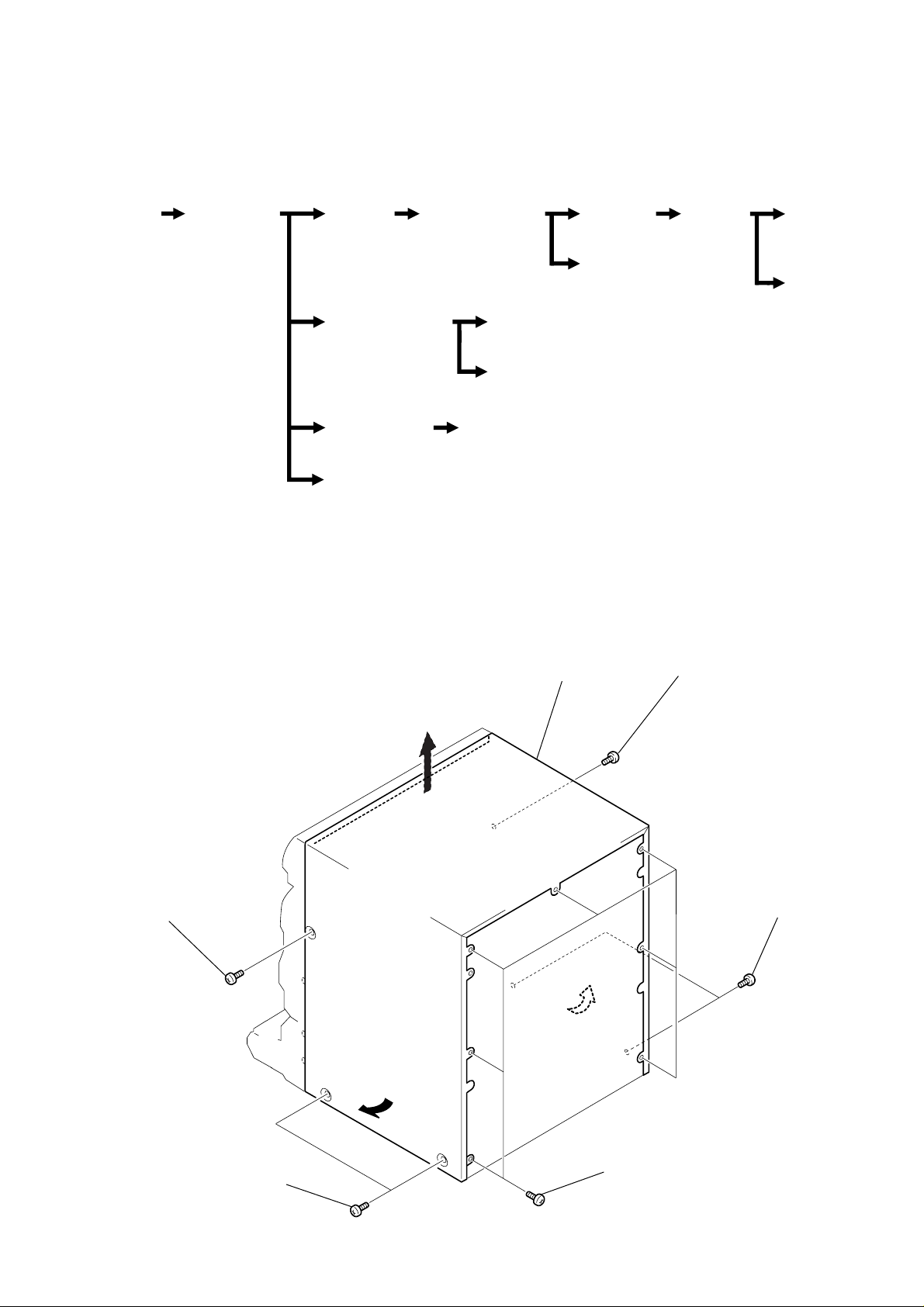
• This set can be disassembled in the order shown below.
SECTION 2
DISASSEMBLY
CASE
(Page 7)
Note: Follow the disassembly procedure in the numerical order given.
FRONT PANEL
SECTION
(Page 8)
MAIN
SECTION
(Page 9)
TAPE MECHANISM
DECK SECTION
(TCM-220WR2)
(Page 10)
CD LID ASS’Y
SECTION
(Page 11)
MAIN BOARD
(Page 8)
CD MECHANISM
DECK SECTION
(CDM37L-5BD21AL)
(Page 9)
PANEL (A)/(B)
SUB ASS’Y
(Page 11)
2-1. CASE
BASE UNIT
(BU-5BD21AL)
(Page 12)
DISC TABLE
(Page 12)
CAPSTAN MOTOR (M1)
(Page 14)
CASSETTE
LID ASS’Y
(Page 10)
3
case
BD BOARD
(Page 13)
1
screw
(case 3 TP2)
OPTICAL
PICK-UP
(KSS-213D/Q-NP)
(Page 13)
SLED
MOTOR (M102),
SPINDLE
MOTOR (M101)
(Page 13)
1
screw
(case 3 TP2)
1
two screws
(case 3 point)
— 7 —
2
seven screws
(BVTT 3
1
two screws
(case 3 point
×
6)
)
2-2. FRONT PANEL SECTION
1
3
front panel section
1
flat wire (11 core)
(CN206)
flat wire (21 core)
(CN205)
1
flat wire (17 core)
(CN102)
2
four screws
(BVTP 3 × 8)
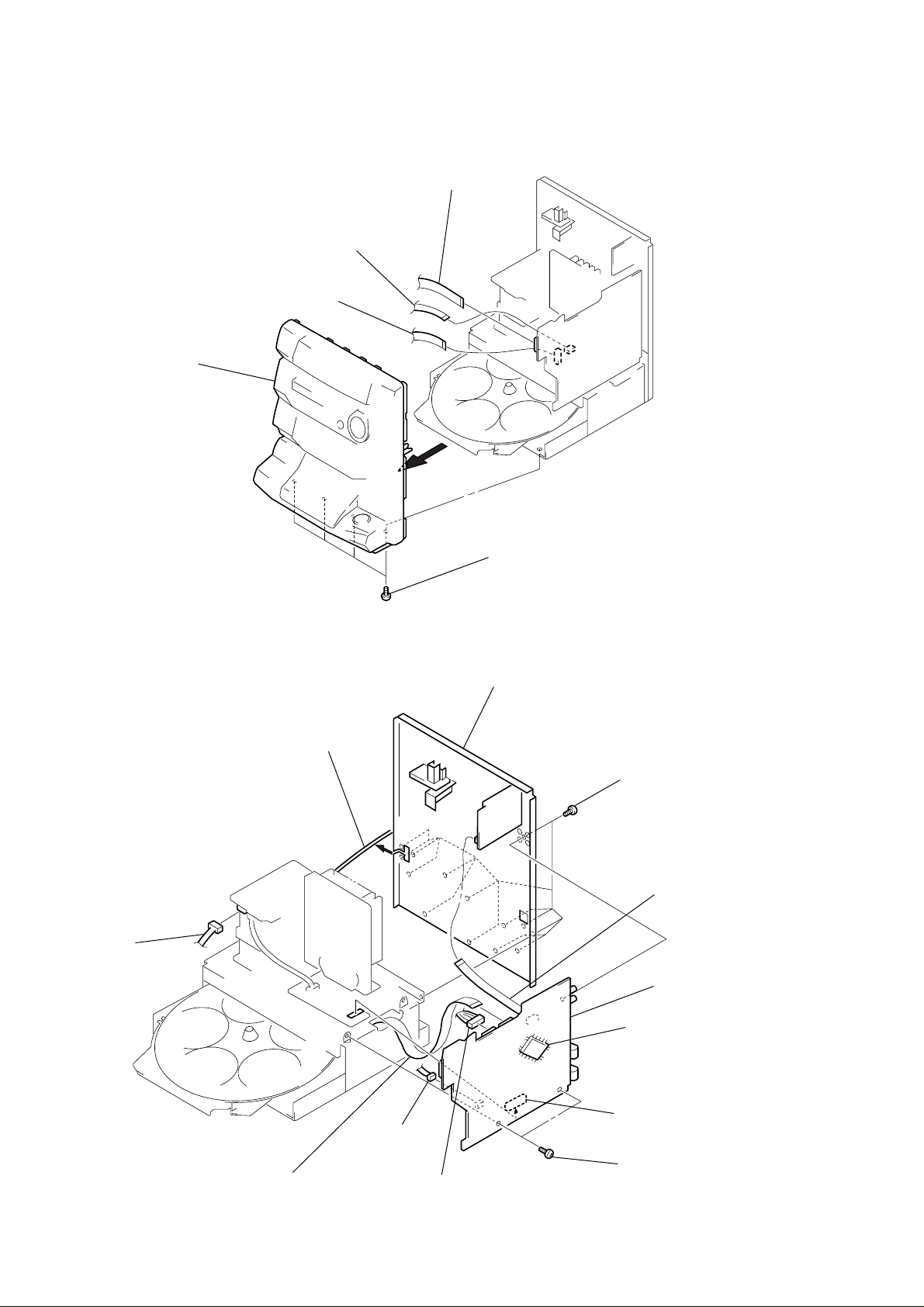
2-3. MAIN BOARD
5
connector
(CN901)
3
power cord
4
back panel
2
fourteen screws
(BVTP 3
1
flat wire (13 core
(CN1)
8
MAIN board
IC201
×
8)
5
flat wire (13 core)
(CN202)
1
connector
(CN106)
5
connector
(CN203)
— 8 —
7
connector
(CN101)
6
two screws
(BVTP 3
×
8)

2-4. MAIN SECTION
)
3
two screws
(BVTP 3
×
8)
2
connector
(CN203)
1
flat wire (13 core)
(CN202)
4
main section
3
eight screws
(BVTP 3
3
two screws
(BVTP 3
×
8
×
8)
2-5. CD MECHANISM DECK SECTION (CDM37L-5BD21AL)
2
five screws
(BVTP 3 × 8)
3
CD mechanism
deck section
(CDM37A-5BD21AL)
4
flat wire (29 core)
(CN101)
— 9 —
1
Open the clamp.
2-6. TAPE MECHANSM DECK SECTION (TCM-220WR2)
)
4
4
three screws
(BVTP 2.6
3
flat wire (21 core)
(CN601)
3
flat wore (11 core)
(CN1001)
×
8)
A
three screws
(BVTP 2.6
×
8)
5
Remove the tape mechanism
deck section (TCM-220WR2)
to derection of the arrow
A
.
2
Open the
cassette lids.
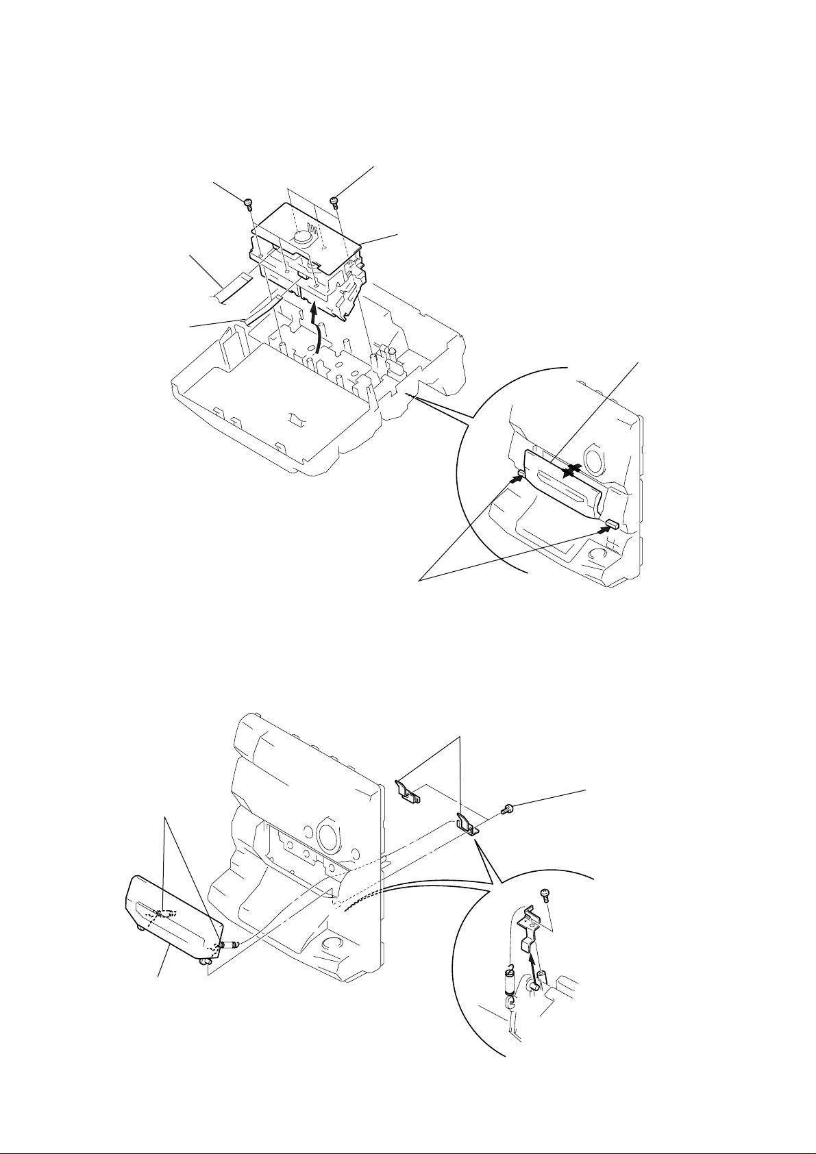
2-7. CASSETTE LID ASS’Y
1
two springs
4
cassette lid ass y
1
Push the
two buttons.
3
two brackets
2
two screws
(BVTP 2.6 × 8
— 10 —

2-8. CD LID ASS’Y SECTION
)
)
5
connector
(CN671)
6
four screws
(BVTP 2.6
×
8)
7
CD lid ass y
4
connector
(CN661)
2
four screws
(BVTP 2.6
×
8
2-9. PANEL (A) / (B) SUB ASS’Y
3
two claws
3
two claws
1
connector
(CN642)
3
CD-B1 SW board
1
connector
(CN612)
2
four screws
(BVTP 2.6 × 8
4
panel (A) sub ass y
5
two claws
6
panel (B) sub ass y
— 11 —
5
two claws
2-10. BASE UNIT (BU-5BD21AL)
e
3
base unit
(BU-5BD21AL)
2
2-11. DISC TABLE
Note:
When the disc table is installed, adjust the positions
of roller cam amd mark ( as shown in the figure, then
set to the groove of disc table.
A
boss
1
screw
(BVTP 3 × 8)
2
bracket (BU)
1
screw
(BVTP 3 × 8)
1
yoke bracket
3
step screw
4
disc tabl
— 12 —
A
2-12. BD BOARD
)
1
two screws
(PTPWH M2.6
3
two springs
5
screw
(BVTP 2.6
6
×
6)
2
3
two springs
4
flat wire (16 core)
7
(S101)
(CN102)
BD board
×
8)
Removal
four solders. limit switch
1
two screws
(PTPWH M2.6
optical pick-up
section
×
6
2-13. OPTICAL PICK-UP (KSS-213D/Q-NP), SLED MOTOR (M102), SPINDLE MOTOR (M101)
3
optical pick-up (KSS-213D/Q-NP)
6
spindle motor
2
sled shaft
(M101)
1
claw
5
4
two screws
(P2
sled motor
(M102)
×
3)
— 13 —
2-14. CAPSTAN MOTOR (M1)
2
3
Removal the AUDIO board
to direction of the arrow A.
1
connector
(CN651)
four screws
(BTP 2.6
×
4)
A
7
Removal the capstan motor (M1)
to direction of the arrow B.
4
Break the soldering
of motor lead.
6
claw
B
5
two screws
(BTP 2.6
×
8)
8
Hang two belts.
— 14 —

SECTION 3
TEST MODE
MC COLD RESET
• The cold reset clears all data including preset data stored in the
RAM to initial conditions. Execute this mode when returning
the set to the customer.
Procedure:
1. Press three buttons GROOVE , ENTER/NEXT , and
DISC 1 simultaneously.
2. The fluorescent indicator tube becomes blank instantaneously,
and the set is reset.
CD DELIVERY MODE
• This mode moves the pick-up to the position durable to vibration.
Use this mode when returning the set to the customer after repair.
Procedure:
1. Press 1/u button to turn the set ON.
2. Press PLAY MODE button and 1/u button simultaneously.
3. A message “LOCK” is displayed on the fluorescent indicator
tube, and the CD delivery mode is set.
MC HOT RESET
• This mode resets the set with the preset data kept stored in the
memory. The hot reset mode functions same as if the power
cord is plugged in and out.
Procedure:
1. Press three buttons GROOVE , ENTER/NEXT , and
DISC 2 simultaneously.
2. The fluorescent indicator tube becomes blank instantaneously,
and the set is reset.
SLED SERVO MODE
• This mode can run the CD sled motor freely. Use this mode, for
instance, when cleaning the pick-up.
Procedure:
1. Select the function “CD”.
2. Press three buttons GROOVE , ENTER/NEXT , and
CD FLASH simultaneously.
3. The Sled Servo mode is selected, if “CD” is blinking on the
fluorescent indicator tube.
4. With the CD in stop status, press ) button in CD section to
move the pick-up to outside track, or 0 button to inside track.
5. To exit from this mode, perform as follows:
1) Move the pick-up to the most inside track.
2) Press three buttons in the same manner as step 2.
Note:
• Always move the pick-up to most inside track when exiting
from this mode. Otherwise, a disc will not be unloaded.
• Do not run the sled motor excessively, otherwise the gear can
be chipped.
CHANGE-OVER OF AM TUNER STEP BETWEEN 9 kHz
AND 10 kHz
• A step of AM channels can be changed over between 9 kHz and
10 kHz.
Procedure:
1. Press 1/u button to turn the set ON.
2. Select the function “TUNER”, and press TUNER/BAND
button to select the BAND “AM”.
3. Press 1/u button to turn the set OFF.
4. Press ENTER/NEXT and 1/u buttons simultaneously, and
the display of fluorescent indicator tube changes to “AM 9 k
STEP” or “AM 10 k STEP”, and thus the channel step is changed
over.
Be sure not to change with carelessness.
LED AND FLUORESCENT INDICA TOR TUBE ALL LIT, KEY
CHECK MODE
Procedure:
1. Press three buttons GROOVE , ENTER/NEXT , and
DISC 3 simultaneously.
2. LEDs and fluorescent indicator tube are all turned on.
Press DISC 2 button, and the key check mode is activated.
3. In the key check mode, the fluorescent indicator tube displays
“K 1 J0 V0”. Each time a button is pressed, “K”value increases.
However, once a button is pressed, it is no longer taken into
account.
“J” value increases like 1, 2, 3 ... if rotating JOG dial knob in
“clock wise” direction, or it decreases like 0, 9, 8 ... if rotating
in “counter clock wise” direction.
“V” value increases like 1, 2, 3 ... if rotating VOLUME knob
in “+” direction, or it decreases like 0, 9, 8 ... if rotating in “–”
direction.
4. To exit from this mode, press three buttons in the same manner
as step 1, or disconnect the power cord.
SELF-DIAGNOSIS
This model has the self-diagnosis function for the video and audio
decoder sections.
Immediately after the power on, the self-diagnosis function searches
each operation of IC’s around the mechanism controller (IC701).
The LED (D701) on the VIDEO board indicates their results.
LED (D701) INDICATION SYMPTOM
Light No error
1 time blinking (Repeatedly) External RAM (S-RAM) error
(IC751)
2 times blinking (Repeatedly) Video decoder section error
(IC201)
3 times blinking (Repeatedly) Video RAM (D-RAM) error
(IC251)
4 times blinking (Repeatedly) Audio decoder section error
(IC201)
[VIDEO BOARD] (SIDE-A)
— 15 —
IC701
D701
IC771
IC201
IC901

VERSION CHECK MODE
Procedure:
1. Press three buttons GROOVE , ENTER/NEXT , and DISC 3
simultaneously.
2. LEDs and fluorescent indicator tube are all turned on.
Press DISC 1 button, and the version check mode is activated.
3. In the version check mode, the fluorescent indicator tube displays
version information as follows.
SPEC ASIA-2←
Press DISC 1 ↓
MC F/V V1.3
Press DISC 1 ↓ Press
VC F/V V1.4 DISC 1
Press DISC 1 ↓
GC S-V V1.0
Press DISC 1 ↓
LBT 715 VCD
4. T o exit from this mode, press three buttons in the same manner
as step 1, or disconnect the power cord.
AGING MODE
This mode can be used for operation check of CD section and tape
deck section.
• If an error occurred:
The aging operation stops.
• If no error occurs:
The aging operation continues repeatedly.
1. Aging Mode in CD Section
1-1. Operating Method of Aging Mode
1. Set discs in DISC 1 and DISC 3 trays.
2. Select the function “CD”.
3. Press three buttons GROOVE , ENTER/NEXT ,
and DISC 5 simultaneously.
4. The aging mode is activated, if a changer mark on the
fluorescent indicator tube is blinking.
5. In the aging mode, the aging is executed in a sequence given
in “1-2. Operation during Aging Mode”.
The aging continues unless an alarm occurred.
6. To exit from the aging mode, press 1/u button to turn the
set OFF.
• If a button other than buttons In CD section is pressed during
aging, the aging in the CD section is finished.
• To execute aging to the tape deck section successively,
press · button in the deck A.
“AGING” is displayed on the fluorescent indicator tube. (For
the aging in tape deck, see “2. Aging Mode in Tape Deck
Section”.
1-2. Operation during aging Mode
In the aging mode, the program is executed in the following
sequence.
1. The disc tray turns to select a disc. (For a disc selection
sequence, see Section 1-3.)
2. TOC of disc is read.
3. The pick-up accesses to the last track.
4. Steps 1 through 3 are repeated.
1-3. Disc Selection Sequence
• During the aging mode, discs are selected in the following
sequence:
Disc 1 → Disc 3
↑ ↓
Disc 3 ← Disc 1
2. Aging Mode in Tape Deck Section
2-1. Operating Method of Aging Mode
1. Load a commercially available 10-minute tape into the decks
A and B respectively.
(If a 10-minute tape is not available, another tape may be
used but a cycle time will be longer.)
2. Select the function “TAPE”.
3. Rewind tapes in advance by pressing 0 button
respectively on decks A and B.
4. Press three buttons GROOVE , ENTER/NEXT ,
and DISC 5 simultaneously.
5. Press · button on deck A. (This button triggers the aging
mode.)
6. The aging mode is activated if “AGING A” is displayed on
the fluorescent indicator tube.
7. In the aging mode, the aging is executed in a sequence given
in “2-2. Operation during Aging Mode”.
The aging continues unless an alarm occurred.
8. T o exit from the aging mode, press 1/u button to turn the
set OFF.
2-2. Operation during Aging Mode
In the aging mode, the program is executed in the following
sequence.
1. A tape on FWD side is played for one minute.
2. PAUSE STOP is made.
3. Recording is made for 3 minutes. (For the deck not having
the record function, the play is executed. In this case, ·
LED does not light up.)
4. FF is executed up to the end of tape.
5. A tape is reversed, and the tape on REV side is played for
one minute.
6. PAUSE STOP is made.
7. Recording is made for 3 minutes. (For the deck not having
the record function, the play is executed. In this case, ª
LED does not light up.)
8. FF is executed up to the end of tape.
9. Steps 1 through 8 are executed for the other deck.
10. Steps 1 through 9 are repeated unless an alarm occurred.
2-3. Deck Selection Sequence
• During the aging mode, decks are selected in the following
sequence:
Deck A (FWD) → Deck A (REV)
↑ ↓
Deck B (REV) ← Deck B (FWD)
— 16 —

VIDEO CD COLOR BAR MODE
On this mode, the data of the color bar signal as a picture signal and
the 1 kHz sine wave signal as a sound signal are output by the
mechanism controller (IC701) for the video CD signal check. When
measurement of the voltage and waveform on the VIDEO board,
perform it in this mode.
For reference, the color bar signal can be observed at J9001 (VIDEO
OUT) and the sound signal can be observed at J101 (VIDEO
(AUDIO) OUT) using an oscilloscope.
Procedure:
1. Turned power switch on.
2. Press the FUNCTION button to select the CD.
3. Connect the SL701 on the VIDEO board with solder.
4. After measuring, remove the soldering installed.
oscilloscope
E-F BALANCE MODE
Refer to the SECTION 6 ELECTRICAL ADJUSTMENTS page
21.
Procedure:
1. Turned power switch on.
2. Press the FUNCTION button to select the CD.
3. Connect the SL701 and SL703 on the VIDEO board with solder.
4. Press the · button in playback.
5. Press the REPEAT button, the tracking servo and sledding
servo are turned on or off.
6. When the servo is off, the counter on front panel will not be
changed.
7. After measuring, remove the soldering installed.
set
B
A
C
75
Ω
J9001 (VIDEO OUT)
H
+
–
A = 0.9 to 1.1 Vp-p
B = 0.678 to 0.75 Vp-p
C = 0.214 to 0.328 Vp-p
Fig. 1 Video CD Color Bar Signal Output from J9001
(VIDEO OUT)
[VIDEO BOARD] (SIDE-B)
SL703
SL702
SL701
IC751
IC251
— 17 —
SECTION 4
r
MECHANICAL ADJUSTMENTS
SECTION 5
ELECTRICAL ADJUSTMENTS
PRECAUTION
1. Clean the following parts with a denatured-alcohol-moistened
swab:
record/playback head pinch roller
erase head rubber belts
capstan idlers
2. Demagnetize the record/playback head with a head
demagnetizer.
3. Do not use a magnetized screwdriver for the adjustments.
4. After the adjustments, apply suitable locking compound to the
parts adjusted.
5. The adjustments should be performed with the rated power
supply voltage unless otherwise noted.
• Torque Measurement
Mode Torque Meter Meter Reading
Forward CQ-102C
Forward
Back Tension (0.026 – 0.082 oz•inch)
Reverse CQ-102RC
Reverse
Back Tension (0.026 – 0.082 oz•inch)
FF, REW CQ-201B
CQ-102C
CQ-102RC
36 to 61g•cm
(0.50 – 0.84 oz•inch)
2 to 6g•cm
36 to 61g•cm
(0.50 – 0.84 oz•inch)
2 to 6g•cm
61 to 143g•cm
(0.85 – 1.98 oz•inch)
DECK SECTION
0 dB=0.775 V
1. Demagnetize the record/playback head with a head
demagnetizer. (Do not bring the head demagnetizer close to
the erase head.)
2. Do not use a magnetized screwdriver for the adjustments.
3. After the adjustments, apply suitable locking compound to the
parts adjust.
4. The adjustments should be performed with the rated power
supply voltage unless otherwise noted.
5. The adjustments should be performed in the order given in this
service manual. (As a general rule, playback circuit adjustment
should be completed before performing recording circuit
adjustment.)
6. The adjustments should be performed for both L-CH and Rch.
7. Switches and controls should be set as follows unless otherwise
specified.
8. Set to test mode. (Press key switch same time
GROOVE ENTER/NEXT and DISC 4 buttons.)
To exit from the test mode, press the 1/u button.
• Test Tape
Tape Signal Used for
P-4-A100 10 kHz, –10 dB Azimuth Adjustment
WS-48B 3 kHz, 0 dB Tape Speed Adjustment
P-4-L300 315 Hz, 0 dB Level Adjustment
• T ape Tension Measurement
Mode Tension Meter Meter Reading
Forward CQ-403A more than 100 g (3.53 oz)
Reverse CQ-403R more than 100 g (3.53 oz)
Record/Playback Head Azimuth Adjustment
DECK A DECK B
Note: Perform this adjustments f or both dec ks .
Procedure:
1. Mode: Playback (FWD)
test tape
P-4-A100
(10 kHz, –10 dB)
set
MAIN board
CN207
3
(L-CH)
pin
1
(R-CH)
pin
MAIN board
CN207
pin
2
(GND)
level mete
+
–
2. Turn the adjustment screw and check output peaks. If the peaks
do not match for L-CH and R-CH, turn the adjustment screw
so
that outputs match within 1 dB of peak.
output
level
within
1 dB
within
1 dB
L-CH
peak
R-CH
Screw
position
peak
L-CH
peak
R-CH
peak
Screw
position
— 18 —

3. Mode: Playback (FWD)
e
e
+
–
set
test tape
P-4-L300
(315 Hz, 0 dB)
MAIN board
CN207 (pin
3
: L-CH)
(pin
1
: R-CH)
level meter
test tape
P-4-A100
(10 kHz, –10 dB)
set
pin
waveform of oscilloscope
in phase 45°90°135°180
MAIN board
CN207
pin
pin 2 (GND)
1
(R-CH)
good
3
(L-CH)
oscilloscop
V
wrong
Tape Speed Adjustment DECK A
Note: Start the Tape Speed adjustment as below after setting to the test
mode.
In the test mode, the tape speed is high during press the
H SPEED DUB button.
Procedure:
H
1. Turn the power switch on.
2. Press the GROOVE button, ENTER/NEXT button and
DISC 4 button simultaneously.
To exit from the test mode, press the 1/u button.
Mode: Playback (FWD)
test tape
WS-48B
(3 kHz, 0 dB)
°
set
frequency counter
+
–
4. Repeat steps 1 to 3 in playback (REV) mode.
5. After the adjustments, apply suitable locking compound to the
parts adjusted.
Adjustment Location : Playback Head (Deck A)
Record/Playback Head (Deck B)
revers
forward
MAIN board
CN207 (pin
(pin
3
: L-CH)
1
:R-CH)
1. Insert the WS-48B into the deck A and the blank tape into the
deck B.
2. Press the r REC button and · button on the deck B. Then
the deck B is at recording mode.
3. Set the deck A to playback mode.
4. Press the H SPEED DUB button in playback mode.
Then at high speed mode.
5. Adjust RV652 on the AUDIO board so that frequency counter
reads 6,000 ± 180 Hz.
6. Press the H SPEED DUB button.
Then at normal speed mode.
7. Adjust R V651 on the AUDIO board so that frequency counter
reads 3,000 ± 90 Hz.
8. Frequency difference between deck A and deck B the beginning
of the tape should be within ± 1.5 %.
Adjustment Location: AUDIO board (See page 20)
Sample Value of Wow and Flutter: 0.3% or less W.RMS
(WS-48B)
Playback level Adjustment DECK A DECK B
Procedure:
Mode: Playback (FWD)
Deck A is RV311 (L-CH) and RV411 (R-CH), Deck B is RV301
(L-CH) and RV401 (R-CH) so that adjustment within adjustment
level as follows.
Adjustment Level:
CN207 PB level: 301.5 to 338.3 mV (– 8.2 to – 7.2 dB) level
difference between the channels: within ± 0.5 dB
Adjustment Location: AUDIO board (See page 20)
— 19 —
Record bias Current Adjustment DECK B
r
r
5
Procedure:
1. Mode: Record
Adjustment and Connection Location:
[AUDIO BOARD] (Conductor Side)
pin 6 (L-CH) of IC1501 on the MAIN board.
pin
#¶
(R-CH) of IC1501 on the MAIN board.
1) 315 Hz
2) 10 kHz
AF OSC
attenuator
pin 2 (GND) of CN207 on the MAIN board.
50 mV (–23.8 dB)
Ω
600
set
blank tape
CS-123
2. Mode: Playback
recorded
portion
set
MAIN board
CN207 (pin
(pin
3
1
: L-CH)
: R-CH)
level mete
+
–
Confirm playback the signal recorded in step 1 become adjustable
limits as follows.
If these levels do not adjustable limits, adjustment the RV341 (LCH) and R V441 (R-CH) on the AUDIO board to repeat steps 1 and
2.
Adjustable limits: Playback output of 315 Hz to playback
output of 10 kHz: ±0.5 dB
Adjustment Location: AUDIO board
Record Level Adjustment DECK B
Procedure:
1. Mode: Record
pin
6
(L-CH) of IC1501 on the MAIN board.
pin
#¶
(R-CH) of IC1501 on the MAIN board.
AF OSC
315 Hz, 50 mV (–23.8 dB)
Ω
attenuator
600
blank tape
CS-123
set
RECORD
BAIS
L
RV301
RV401®R
PB LEVEL
[MAIN BOARD] (Component Side)
R
®
L
RV441RV341
– DECK B –
IC201
IC301
TAPE SPEED
(NORMAL)
RV651
®
PB
LEVEL
1
CN207
RECORD LEVEL
– DECK A –
RV1501
21 1
3
IC1501
22 42
RV1551
(HIGH)
RV652
RV311
L
RV411
R
®
®
®
CN20
pin
2
(GND) of CN207 on the MAIN board.
2. Mode: Playback
recorded
portion
set
MAIN board
CN207 (pin
(pin
3
1
: L-CH)
: R-CH)
level mete
+
–
Confirm playback the signal recorded in step 1 become adjustable
limits as follows.
If these levels do not adjustable limits, adjustment the RV1501 (LCH) and R V1551 (R-CH) on the MAIN board to repeat steps 1 and
2.
Adjustable limits:
CN207 PB level: 47.3 to 53.1 mV (–24.3 to –23.3 dB)
Adjustment Location: MAIN board
— 20 —

HCD-V3900/V5900
e
e
e
e
+
–
TP (PLCK)
BD board
frequency counter
r
CD SECTION
Notes:
1. CD block basically constructed to operate without adjustment. Therefore, check each item in order given.
2. Use YEDS-18 disc (Part No.: 3-702-101-01) unless otherwise indicated.
3. Use the oscilloscope with more than 10 MΩ impedance.
4. Clean an object lens by an applicator with neutral detergent when the
signal level is low than specified value with the following checks.
S-Curve Check
Connection:
oscilloscop
BD board
TP (FE)
TP (VC)
+
–
Procedure:
1. Connect the oscilloscope to TP (FE) and TP (VC) on BD board.
2. Connect the TP (FEI) and TP (VC) with lead wire.
3. Turned power switch on.
4. Put disc (YEDS-18) in and turned power switch on again and
actuate the focus search.
5. Confirm that the oscilloscope waveform (S-curve) is
symmetrical between A and B. And confirm peak to peak level
within 3.0 ± 1.0 Vp-p.
S-curve waveform
symmetry
A
within 3.0
B
±
1.0 Vp-p
RF signal waveform
VOLT/DIV: 200 mV
TIME/DIV: 500 ns
(with the 10: 1 prob
in use)
level: 1.3 Vp-p
+0.25
–0.20
When observing the eye pattern, set the oscilloscope for AC range
and raise vertical sensitivity.
E-F Balance (Traverse) Check
Connection:
oscilloscop
(DC range)
BD board
TP (TE)
TP (VC)
+
–
Procedure:
1. Connect the oscilloscope to TP (TE) and TP (VC) on BD board.
2. Turned power switch on.
3. Connect the SL702 and SL703 on the VIDEO board with solder.
4. Put disc (YEDS-18) in and press the · button, and play the
number five track.
5. Press the REPEA T button. (The tracking servo and the sledding
servo are turned off.)
6. Confirm that the level B of the oscilloscope’s waveform and
the A (DC voltage) of the center of the traverse waveform.
Confirm the following:
A/B × 100 = less than ±22 %
Traverse waveform
Center of the waveform
RF PLL Free-run Frequency Check
Connection:
Procedure:
1. Connect the frquency counter to TP (PLCK) on the BD board.
2. Turned power switch on.
3. Put disc (YEDS-18) in and press the · button, and play the
number five track.
4. Confirm that the reading on frequency counter is 4.3218 MHz.
Connection Location:
[BD BOARD] (SIDE-A)
(FEI)
(FE)
(TE)
(PLCK)
IC103
IC101
(RF)
(VC)
VIDEO SECTION
Frequency Adjustment
Connection:
VIDEO board
TP410 (DCLK)
Procedure:
1. Connect the frequency counter to TP410 (DCLK) on VIDEO
board.
2. Turned power switch on.
3. Press the FUNCTION button to select the CD.
4. Adjust CT401 on the VIDEO board so that the frequency counter
reading 13.5 MHz ± 40 Hz at stop status.
Adjustment Location:
[VIDEO BOARD] (SIDE-B)
frequency counte
+
–
CT401
TP410
(DCLK)
IC402
6. After check, remove the lead wire connected in step 2.
Note: • Try to measure several times to make sure that the ratio of A : B
or B : A is more than 10 : 7.
• Take sweep time as long as possible and light up the brightness
to obtain best waveform.
RF Level Check
Connection:
oscilloscop
(AC range)
BD board
TP (RF)
TP (VC)
+
–
Procedure:
1. Connect the oscilloscope to TP (RF) and TP (VC) on BD board.
2. Turned power switch on. (stop mode)
3. Put disc (YEDS-18) in and press the · button.
4. Confirm that the oscilloscope waveform is clear and check RF
signal level is correct or not.
Note: Clear RF signal waveform means that the shape “≈” can be clearly
distinguished at the center of the waveform.
B
0V
A (DC voltage)
level: 1.3 ± 0.6 Vp-p
7. Press the REPEA T button. (The tracking servo and the sledding
servo are turned on.) Confirm that the C (DC voltage) is almost
equal to the A (DC voltage) is step 6.
Traverse waveform
0 V
Tracking servo
Sled servo
OFF
Tracking servo
Sled servo
ON
C (DC
voltage)
8. After check, remove the soldering installed in step 3.
— 21 — — 22 —

HCD-V3900/V5900
6-1. BLOCK DIAGRAM – BD SECTION –
SECTION 6
DIAGRAMS
OPTICAL PICK-UP
BLOCK (KSS-213D/Q-NP)
LASER
DIODE
PD
DETECTOR
E
AC
BD
F
LD
TRACKING
COIL
FOCUS
COIL
LD
POWER
1
4
VC
M102
SLED
MOTOR
M101
SPINDLE
MOTOR
LD
DRIVE
Q101
RF AMP
IC103
APC LD
2
AMP
RF FQ
AMP
19
RF
INTEGRATOR
16
15
13
1110
VC
12
INTE-
GRATOR
4
5
19
20
10
9
23
24
VC
1
3
4
5
6
8
9
T+
T–
F+
16
F–
17
13
M
12
27
M
26
RF
SUMMING
AMP
FOCUS
ERROR
AMP
TRACKING
ERROR
AMP
VC
BUFFER
FOCUS/TRACKING COIL DRIVE
SPINDLE/SLED MOTOR DRIVE
IC102
1
2
DIGITAL SERVO
DIGITAL SIGNAL PROCESSOR
IC101
ASY0
39
RF AC
36
ASY1
RF DC
TE
SE
FE
TFDR
TRDR
FFDR
FRDR
SRDR
SFDR
MDP
ASYMMETRY
CORRECTION
A/D
CONVERTER
38
26
27
28
29
4
6
8
10
2
100
96
MIRR
DFCT
FOK
DETECTOR
MIX
FOK
DFCT
MIRR
SERVO DSP
FOCUS
SERVO
TRACKING
SERVO
SLED
SERVO
PWM
GENERATOR
TRACKING
PWM
GENERATOR
FOCUS
PWM
GENERATOR
SLED
PWM
GENERATOR
DIGITAL
PLL
CLOCK
GENERATOR
EFM
DEMODULATOR
62
XTAL
SYNC
PROTECTOR
TIMING
GENERATOR 1
CLV SERVO
PROCESSOR
1B TIMS
OVERSAMPLING
FILTER
NOISE
SHAPER
REGISTER
DATA BUS
ERROR
CORRECTOR
TIMING
GENERATOR 2
PRIORITY
EMCODER
ADDRESS
GENERATOR
32K
RAM
D/A
DATA
PROCESSOR
MUTE
79 54
GFS
DIGITAL
OUT
PEAK
DETECTOR
SERIAL/PARALLEL
PROCESSOR
INTERFACE
S STOP
99
SWITCH
+5V
SERVO
S101
LIMIT
SUBCODE
P-W
PROCESSOR
SUBCODE
Q
PROCESSOR
INTERFACE
SEQUENCER
CPU
SERVO
AUTO
MD2
EXCK
SBSO
SUBQ
SQCK
SCLK
DATA
LRCK
BCLK
SCOR
WFCK
DATA
XLT
CLK
SENS
C2PO
FOK
DFCT
MIRR
XRST
+5V
70
76
75
77
78
83
46
45
47
74
73
86
87
88
80
56
93
92
91
81
LDON
384FS
EXCK
SUBQ
SUBQ
SQCK
SCLK
ADATA
LRCK
BCLK
SCOR
DATA
XLT
CLK
SENS
C2PO
XRST
AMUTE
B
VIDEO
SECTION
(Page 25 )
15MUTE
16
• SIGNAL PATH
: CD
: VIDEO
— 23 — — 24 —

6-2. BLOCK DIAGRAM – VIDEO SECTION –
BUFFER
IC501 (1/2)
B
CD
SECTION
(Page 24)
IC501
(2/2)
B
CD
SECTION
(Page 24)
16
BCK
ADATA
LRCK
C2PO
384FS
ADATA
LRCK
BCLK
28.63636MHz
45.1584MHz
DATA
CLK
AMUTE
384FS
416
384FS
DATA
CLK
AMUTE
SQCK
SUBQ
SCLK
XLT
LDON
SCOR
SENS
XRST
X202
X201
9
8
7
6
5
XTL0O
2
XTL01
3
106
XTL2O
107
XTL2I
73
DATA
78
CLK
74
AMUTE
11
SQCK
10
SUBQ
77
SCLK
XLT
76
75
LDON
71
SCOR
62
SENS
RESET
48
11
12
13
14
15
2–5 7–10 35–38 40–43
•
DQ1
I/O1
38–43 46–55•
•
•11–13 15–19
D0
112
111
110
109
103
100
101
102
D-RAM INTERFACE
17–21 23 24 32 33••••
•
A0
I/O8
2–10 21 23–25
22–29 • 31–3513 – 20
A0
D7
18–21 24–28•
DQ16
D-RAM
IC251
S-RAM
IC751
••
CD-ROM
DECODER
MPEG
AUDIO
DECODER
A0
A12
A12
MPEG DECODER
IC201
7–13 16
LCAS
UCAS
IC772
WE
XTCS
6
54
3
12
40
IC701
MPEG
VIDEO
DECODER
EACH CIRCUIT BLOCK
•
IC771
A17
POSTPROCESSOR
SYNC GENERATOR
HOST INTERFACE
•
120
119
•
D0
D7
AS
5 6
•
A0
A3
MPEG
SYSTEM
DECODER
34
3735
301516 31
W
A8
RAS
CE1
OE
55
RD
272022
8
10 9
11
12
13
41 54 56 43 70 7 8
A18
MECHA CONTROL
VIDEO
&
XHCS
XWR
WR
XHDT
WAIT
117115116114
XHIRQ
Y
C
XHIRQ
EXTAL
71
73
•
76
80
63
70
97
95
92
93
94
89
56
57
58
59
118
DF-XLAT
VDAC-XLAT
XTAL
5251
X701
10MHz
XSGRST
HSYNC
VSYNC
FID
DCLK
XOSDEN
OSD B
OSD G
OSD R
XRST
CLOCK
GENERATOR
IC272
CMD0
CMD1
CMD2
CMD3
SACK
QINT
MREQ
NPIN
Y0-Y7
C0-C7
1
2
3
4
5
6
72
64
OSD B
OSD G
OSD R
XOSDEN
VSYNC
HSYNC
DCLK
SYSTEM SELECT
18
Y
11
27
C
20
18
17
16
15
19
20
CK 1/2 Q
1 5
S9001
RGB-YUV
CONV.
TIMING
GEN.
98 10097
HSYNC
OUTPUT
CONT.
SYNC
CONT.
PAL
AUTO
NTSC
NOISE REDUCTION
REDUSER
MEMORY
DCLKI
93
VSYNC
DCLK
VIDEO
RAM
DATA
34
CMD0
35
CMD1
36
CMD2
37
CMD3
44
SACK
18
QINT
MREQ
43
IC301
NOISE
CONT.
XRST
OSD
IC271
SEL.
6.75MHz
CD-XRST
YUV-RGB
CONV.
DRAM
IF
DATA INPUT
SHIFT
RESISTOR
DISPLAY
POSITION
CONT.
OSC
8
IIC INTERFACE
IC901
HCD-V3900/V5900
10BIT VIDEO D/A CONVERTER
IC401
VIDEO AMP
IC451
&
INTER-
49 504859 60625557 51
CLK
V
Y
C
VDAC-XLAT
24
29325
5 7
3
7
3
4
1
60
67
51
58
29
30
31
4
3
2
1
NR-XCS
MCLK
MDATA
RESET
MDATA
OS-XLAT
MCLK
9
6
•
4
1
18
11
CT401
13.5MHZ
DEMPX, LEVEL
TRANSLATOR
&
INTERPOLTATOR
CLOCK GENARATOR
IC402
56
4
3
X401
27MHz
HSYNC
Y, C/Y, U, V
SELECTOR
POLATOR
CLOSED
CAPTION
ENCODER
SIO & I2O-BUS
CONT.
DATA
LPF
LPF
DELAY
56
1/2
XRST
DCLK
MODULATOR
SYNC
SLOPE
GEN.
SYNC GEN.
TIMING CONT.
XVRST
SUB
CARRIER
GEN.
&
FID
VSYNC
• R CH: Same as L ch
• SIGNAL PATH
: VIDEO
: Y
: CHROMA
: CD
DIGITAL FILTER & D/A CONVERTER
384FS
BUFFER
ADATA
LRCK
BCLK
DATA
CLK
DF-XLAT
68494847
MCLK
MDATA
NR-XCS
OS-XLAT
15
RESET
55
IIC-DATA
56
X2
IIC-CLK
X1
111052
X901
5MHz
AMUTE
XRST
IC181
13
4
1
11
6
3
11
12
10
TIMING
6
CIRCUIT
INPUT PLM
3
4
5
2
MODE
IC101
D/A
CONV.
CLOCK
GENERATOR
MUTE
CIRCUIT
INT
1
21
22
27
25
16
18
L CH
XRST
IIC-DATA
IIC-CLK
X101
33.8688MHz
ACTIVE LPF
IC102
R CH
A
MAIN
SECTION
(Page 27)
J9001
VIDEO OUT
J9002
S VIDEO OUT
— 25 — — 26 —

HCD-V3900/V5900
6-3. BLOCK DIAGRAM – MAIN SECTION –
PHONO
VIDEO
REC
OUT
J761
MIC 1
J762
MIC 2
VIDEO
SECTION
(Page26)
IN
A
ST BLOCK
(A DECK)
(B DECK)
TO
PB
HEAD
REC/PB
HEAD
ERASE
HEAD
L
R
L
R
L
R
CD L CH
IIC DATA
16
IIC CLK
XRST
CN201
HRPE101
J101
HP101
TU L CH
ST DOUT
TUNED
STEREO
ST MUTE
ST DATA
ST CLK
ST CE
R CH
R CH
R CH
22
MIC AMP
IC760
IC101
KEY CONTROL
LPF1
RV341
REC
BIAS
IC501
RV760
MIC VOL
PB EQ
AMP
IC611
PB EQ
AMP
IC601
C331,L331
BIAS
TRAP
EQALIZER/VOLUME
IC201
69
OUT 2
DET
DET
IC202
TABLE
IC201
IN2B
71
IN2A
13
28
10A
PORT A
29
9B
PORT B
30
PORT C
6
61
REC 2B
62
REC 2A
65
KEY OUT 2
64
KEY IN 2
1
IN2
9
IN1
LED
DRIVE
Q201
SELECTOR
IC102
12
OUT
V L
14
CD
15
TC
11
ST
C
IC502
5
A7.5V
4
3
10
SWITCH
Q502
REC
6
DOLBY
B
DOL
PB
PB A/B
NORM/HIGH
BIAS ON/OFF
RM ON/OFF
NR ON/OFF
REC PB/PASS
LM ON/OFF
A120/70
8
12
14
16
17
18
19
20
13
15
M201
TABLE
MOTOR
D201
(DISC No.)
S1005
A CrO2
S1008
B CrO2
SENSOR
MOTOR DRIVE
OUT2
3
M
OUT1
7
9
PAS
NORM/CROM/METAL
15
REC
70
PB
120
10
RV1501
REC(L)
LEVEL
22
4
26 18
MIC AMP
IC760
LPF2
11
25
24
A/D
LOGIC
D/A
7 8 9
STORBE
CLOCK
DATA
SWITCH
Q501
DIGITAL
81
ECHO
IC761
RV761
ECHO
LEVEL
RV311
PB(L)
LEVEL
RV301
PB(L)
LEVEL
IC602
REC/PB SWITCH
1
2
3
Q621,622
R CH
BIAS
OSC
+7.5V
Q623
2
4
17 16
A
B
NORM
CROM
MIX
IC1501
DOLBY NR/REC EQ AMP
REC
EQ
BIAS
SW
S201
UP SW
33
X101
5MHz
BUF IN2
DATA
ST DOUT
TUNED
STEREO
ST MUTE
ST DAYA
ST CLK
ST CE
BB12
BB22
CLOCK32LATCH
34
38
41
40
45F OUT2
39
3
45
44
5
4
55
56
57
66
69
70
72
67
65
68
11
10
87
88
89
90
91
92
93
77
76
96
61
60
62
LATCH
COM CLK
COM DATA
K CON ON
K CON LAT
IIC DATA
IIC CLK
XRST
ST DOUT
TUNED
STEREO
ST MUTE
ST DAYA
ST CLK
ST CE
X1
X2
PB A/B
EQ H/N
BIAS
REC MUTE
NR ON/OFF
R/P PASS
TC MUTE
UP SW
T SENS
TC RELAY
TBL R
TBL L
TRAY LED
SPEANA
IC231
V5900 ONLY
Q201
MAIN CONTROL
IC301
A PLAY SW
B PLAY SW
CAP M ON/OFF
FEED
BACK
Q203
DBFB
SWITCH
Q202
D309
SW F CON
DBFB H/L
TA MUTE
XRST
CD POWER
AC CUT
A SHUT
A HALF SW
B HALF SW
B SHUT
TRG LOW
B TRG
A TRG
CAP M H/L
D291
MUTE
CONT
Q231,232
99
2
1
100STK MUTE
6F RELAY
98POWER
57
46
15RESET
20
94
26
97
28
95
27
85
84
83
86
82
+5V
S1001
A PLAY
S1002
B PLAY
RESET
SWITCH
Q301
S1004
A HALF
S1007
B HALF
SWITCH
Q1534,1535
CAPSTAN
MOTOR
SWITCH
Q1531,1532
SWITCH
Q1533
+5V
+5V
MUTE
Q204
+5V
+5V
4
VZ
6
IN2
IN1
5
SPEED
CONTROL
Q651
STANDBY
SWITCH
Q283
RELAY
SWITCH
Q281
Q1001
ROTATION
DET A
S1006
REC A
S1009
REC B
Q1002
ROTATION
DET B
IC1502
TRIGGER
MOTOR DRIVE
RV651
TAPE
SPEED
(NOMAL)
POWER AMP
OUT1
OUT2
RV652
TAPE
SPEED
(HIGH)
IC801
TM131
+
IC9001
IC9002
-11.5V
REG
REG
IC903
REG
IC902
REG
L
FRONT
R
+
TM132
+
L
SURROUND
R
+
V3900 ONLY
FAN
V5900 ONLY
J760
HEADPHONS
LOW
FREQ
HIGH
FREQ
MID
FREQ
S601-608
FUNCTION
KEY
S651-659
FUNCTION
KEY
S609-615
FUNCTION
KEY
S676-679
FUNCTION
S681-686
FUNCTION
S616-618
FUNCTION
S641-647
FUNCTION
13
S661-666
FUNCTION
S619-626,628-633
FUNCTION
S667-671
FUNCTION
+B
-B
D906
D907
+5V
13
+5V
13
+5V
13
+7V
13
IC904
+12V
REG
-32V
KEY
KEY
KEY
KEY
KEY
KEY
KEY
D901
D902-905
VOLUME
S701
JOG
S711
F1
F2
RELAY
DRIVE
M2
MOTOR
M1
D+5V
(UNSW)
D+5V
(SW)
A+5V
(SW)
+3.3V
Q141,142
2
PROTECTOR
1
7
RESET
IC302
IC281
AC OFF
A+7.5V
A-7.5V
+5V
(UNSW)
DVDD
RDS
D+5V
IC801
+3.3V
REG
RY141
R-CH
6
4
R-CH
FAN
DRIVE
Q191,192
R-CH
IC901
1
VCC
+7.5V
VDD
D+5V
ST +10V
Q905
Q901
Q9001
Q9003
VP
2
VEE
9
EN
4
D901
D303
D914
Q903
+10V
REG
REG
Q904
10
POWER
CONT
Q907
POWER
CONT
Q906
POWER
CONT
Q902
13
POWER
CONT
Q9002
POWER
13
CONT
Q9004
µCOM D+5V
CD M+7V
(UNSW)
TC M+12V
OVER LOAD
SENSOR
Q801
OVER LOAD
DET
Q282
TO
MPEG
2
TRIGGER
M
10
CAPSTAN
M
MOTOR
X601
8MHz
S691
DOOR
• RCH Same as L CH
• Signal Path
DISPLAY CONTROL
8
XOUT
9
XIN
36
SPEANA 1
37
SPEANA 2
38
L+R
24
DATA
23
CLOCK
10
RESET
27
KEY1
28
KEY2
20
VOL A
34
VOL B
22
JOG A
35
JOG B
29
KEY3
21
DOOR SW
30
KEY4
KEY4
T901
T901
: FM
: PHONO
: CD
: PB (DECK A)
: PB (DECK B)
: REC (DECK B)
IC601
SEG1
SEG21
GR15
LED11
LED12
LED13
LED SELECT
LED15
LED16
LED17
F901
S901
F902
GR1
LED7
LED8
LED4
LED4
LED5
LED6
57
77
42
56
79LED1
80LED2
1LED3
2LED4
5
6
14
15
16
17
25
2
3
4
18
19
31
33SIRCS
78VKK
LED3
VP
FLOURESCENT
INDICATOR TUBE
VF1
LED
DRIVE
Q604-612
SELECT
SWITCH
Q601-603
LED
DRIVE
Q618
LED
DRIVE
Q619,621
LED
DRIVE
Q614
LED
DRIVE
Q617
LED
DRIVE
Q620
2
AC
IN
D646
FL601
SIRCS
IC602
VF2
D611-625,627
D645,647
D635-638
D631,632
D641,642
D643,644
— 27 — — 28 —
HCD-V3900/V5900
T
T
1 IC301 !º (X2)
2 IC301 !¢ (XT1)
5.6Vp-p
5MHz
2.3 Vp-p
32.768 kHz
6-4. CIRCUIT BOARDS LOCATION
TRANS board
PANEL board
HP/MIC board
TC-A SW
board
LED board
CD-A SW board
DOOR SW board
MOTOR board
CD-B2 SW board
VIDEO POWER board
TC-B SW board
CD-B1 SW board
LEAF SWITCH
board
ENCAPSULATED COMPONEN
(FM/AM TUNER UNIT)
KEY-CON board
MAIN board
AMP board
VIDEO board
THIS NOTE IS COMMON FOR PRINTED WIRING
BOARDS AND SCHEMATIC DIAGRAMS.
(In addition to this necessary note is printed in each
block.)
For schematic diagrams.
Note:
• All capacitors are in µF unless otherwise noted. pF: µµF
50 WV or less are not indicated except for electrolytics
and tantalums.
• All resistors are in Ω and 1/
specified.
• % : indicates tolerance.
¢
•
: internal component.
• 2 : nonflammable resistor.
• 1 : fusible resistor.
• C : panel designation.
Note:
The components identified by mark ! or dotted
line with mark ! are critical for safety.
Replace only with part
number specified.
• U : B+ Line.
• V : B– Line.
• H : adjustment for repair.
• Voltages and waveforms are dc with respect to ground
under no-signal (detuned) conditions.
• Voltages are taken with a VOM (Input impedance 10 MΩ).
Voltage variations may be noted due to normal production tolerances.
• Waveforms are taken with a oscilloscope.
• Circled numbers refer to waveforms.
• Signal path.
F : FM
g : VIDEO/MD
E : PB (DECK A)
d : PB (DECK B)
G : REC (DECK B)
J : CD
I : PHONO
For printed wiring boards.
Note:
• X : parts extracted from the component side.
®
•
•
• b : Pattern from the side which enables seeing.
: Through hole.
¢
: internal component.
4
W or less unless otherwise
Note:
Les composants identifiés par
une marque ! sont critiques
pour la sécurité.
Ne les remplacer que par une
piéce portant le numéro
spécifié.
– VIDEO SECTION –
1
TP115 LRCK
44.1kHz
2
TP117 BCLK
2.11MHz
3
IC201 2 XLT0O
28.63636MHz
4
5
6
7
8
106
IC201 XLT2O
45MHz
IC201 (£ VSYNC
V
IC201 (™ HSYNC
H
IC271 8 OSCIN
6.75MHz
IC401 @¢ COMPO
4.8Vp-p
4.5Vp-p
4Vp-p
4Vp-p
4.8Vp-p
4.8Vp-p
!™
!£
(TP453 COUT)
!¢
!∞
(TP451 VOUT)
!§
!¶
!•
4.4Vp-p
!ª
TP409 27M
5Vp-p
27MHz
CN 103 5 COUT
0.9Vp-p
H
TP452 YOUT
1.3Vp-p
H
CN103 1 VOUT
0.9Vp-p
H
IC701 %¡ EXTAL
5Vp-p
10MHz
IC901 !º X2
5.4Vp-p
5MHz
TP104 LRCK
4.8Vp-p
44.1kHz
TP102 BCLK
CD MOTOR board
TABLE SENSOR board
• Wavef orm
– DISPLAY SECTION –
1
IC601 8 (X-OUT)
9
BD board
VIDEO OU
8MHz
– MAIN SECTION –
4Vp-p
!º
board
AUDIO board
!¡
BD LED board
— 29 — — 30 —
H
IC401 @ª YOUT
H
IC401 #™ COUT
H
TP410 DCLK
13.5MHz
0.9Vp-p
0.9Vp-p
0.3Vp-p
3.7Vp-p
@º
@¡
4.8Vp-p
2.11MHz
TP101 384FS
1.3Vp-p
16.9MHz
IC101 @¡ XOUT
4Vp-p
33.8MHz
HCD-V3900/V5900
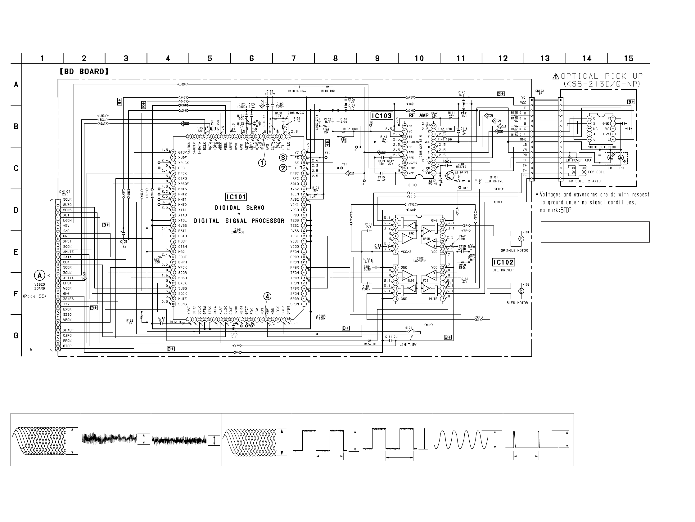
6-5. SCHEMATIC DIAGRAM – BD SECTION – • See page 83 for IC Block Diagrams.
The components identified by mark ! or dotted
line with mark ! are critical for safety.
Replace only with part number specified.
• Waveform
1 IC101 @§ (RFDC)
Approx. 1.3Vp-p
2 IC101 @¶ (TEI)
(PLAY MODE)
Approx. 0.5Vp-p
3 IC101 @ª (FE)
(PLAY MODE)
Approx. 0.2Vp-p
4 IC101 #§ (RFAC)
5 IC101 $∞ (LRCK)
+0.25
1.3
–0.20
Vp-p
22.7 µsec
5.2Vp-p
6 IC101 $¶ (BCLK)
5.2Vp-p
474 nsec
7 IC101 ^™ (XTAI)
16.9344MHz
5.2Vp-p
— 31 — — 32 —
8 IC103 (§ (MDP)
2.4Vp-p
7.5 µsec
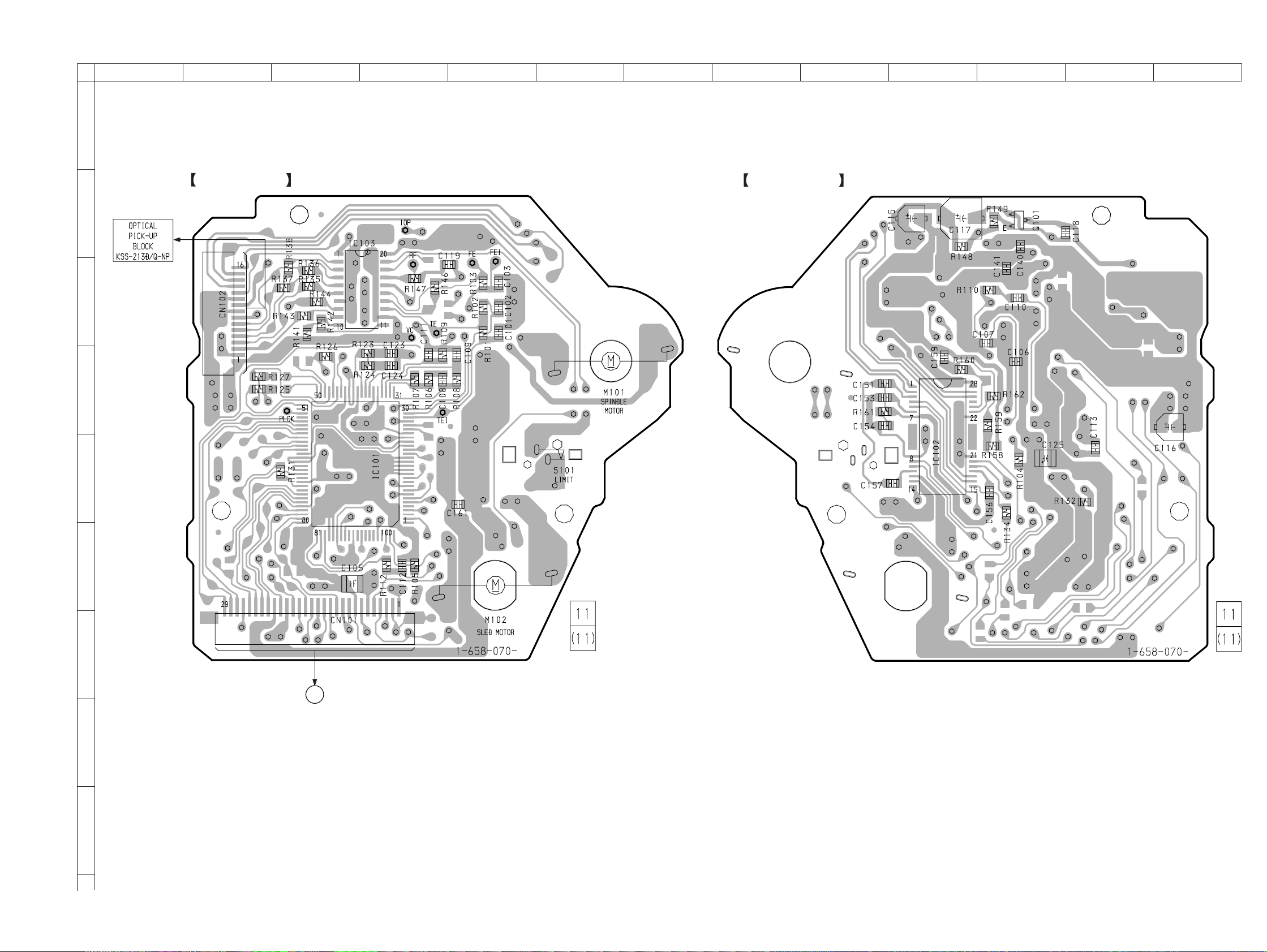
6-6. PRINTED WIRING BOARD – BD SECTION – • See page 29 for Circuit Board Location.
HCD-V3900/V5900
A
B
C
D
12
BD BOARD
(SIDE A)
345678910111213
BD BOARD
(SIDE B)
E
F
G
H
16
A
TO
VIDEO
(Page 51)
I
— 33 —
— 34 —
 Loading...