


BR24C02FV-W
ROHM BR24C02FV-W, BR24C02FJ-W, BR24C02F-W, BR24C02-W, BR24C01AFV-W Datasheet
...
BR24C01A-W / BR24C01AF-W / BR24C01AFJ-W / BR24C01AFV-W / BR24C02-W / BR24C02F-W /
Memory ICs
BR24C02FJ-W / BR24C02FV-W / BR24C04-W / BR24C04F-W / BR24C04FJ-W / BR24C04FV-W
I2C BUS compatible serial EEPROM
BR24C01A-W / BR24C01AF-W / BR24C01AFJ-W /
BR24C01AFV-W / BR24C02-W / BR24C02F-W /
BR24C02FJ-W / BR24C02FV-W / BR24C04-W /
BR24C04F-W / BR24C04FJ-W / BR24C04FV-W
The BR24C01A-W, BR24C02-W, and BR24C04-W series are 2-wire (I2C BUS type) serial EEPROMs which are
electrically programmable.
∗ I2C BUS is a registered trademark of Philips.
!!!!
Applications
VCRs, TVs, printers, car stereos, cordless telephones, short wave radios, programmable DIP switches
!!!!
Features
1) 128×8bits (1k) serial EEPROM.
6) Page write function.
(BR24C01A-W / AF-W / AFJ-W / AFV-W)
256×8bits (2k) serial EEPROM.
(BR24C02-W / F-W / FJ-W / FV-W)
512×8bits (4k) serial EEPROM.
7) DATA security
(BR24C04-W / F-W / FJ-W / FV-W)
2) Two wire serial interface.
3) Operating voltage range : 2.7V∼5.5V
4) Low current consumption
8) Noise filters at SCL and SDA pins.
9) Address can be incremented automatically during
Active (at 5V) : 1.5mA (Typ.)
Standby (at 5V) : 0.1µA (Typ.)
5) Auto erase and auto complete functions can be used
during write operations.
10) Compact packages.
11) Rewriting possible up to 100,000 times
12) Data can be stored for ten years without corruption.
!!!!Absolute maximum ratings (Ta = 25°C)
Parameter Symbol Limits Unit
V
Applied voltage −0.3
Power dissipation
Storage temperature −65
Operating temperature °C
Input voltage
∗1 Reduced by 3.0mW for each increase in Ta of 1°C over 25°C.
∗2 Reduced by 4.5mW for each increase in Ta of 1°C over 25°C.
∗3 Reduced by 8.0mW for each increase in Ta of 1°C over 25°C.
CC
Pd
Tstg
Topr
−
300(SSOP−B8)
450(SOP8, SOP−J8)
800(DIP8)
~+6.5 V
~+125 °C
~+85
−40
−0.3~VCC+0.3
∗1
∗2
∗3
BR24C01A-W / AF-W / AFJ-W / AFV-W : 8 bytes
BR24C02-W / F-W / FJ-W / FV-W : 8 bytes
BR24C04-W / F-W / FJ-W / FV-W : 16 bytes
Write protect feature
Inhibit to WRITE at low V
CC
read operations.
mW
V
BR24C01A-W / BR24C01AF-W / BR24C01AFJ-W / BR24C01AFV-W / BR24C02-W / BR24C02F-W /
Memory ICs
BR24C02FJ-W / BR24C02FV-W / BR24C04-W / BR24C04F-W / BR24C04FJ-W / BR24C04FV-W
!!!!Recommended operating conditions (Ta = 25°C)
Parameter Symbol Limits Unit
Power supply voltage
Input voltage V
CC
V
IN
2.7~5.5 (WRITE)
2.7
~
5.5 (READ)
0~V
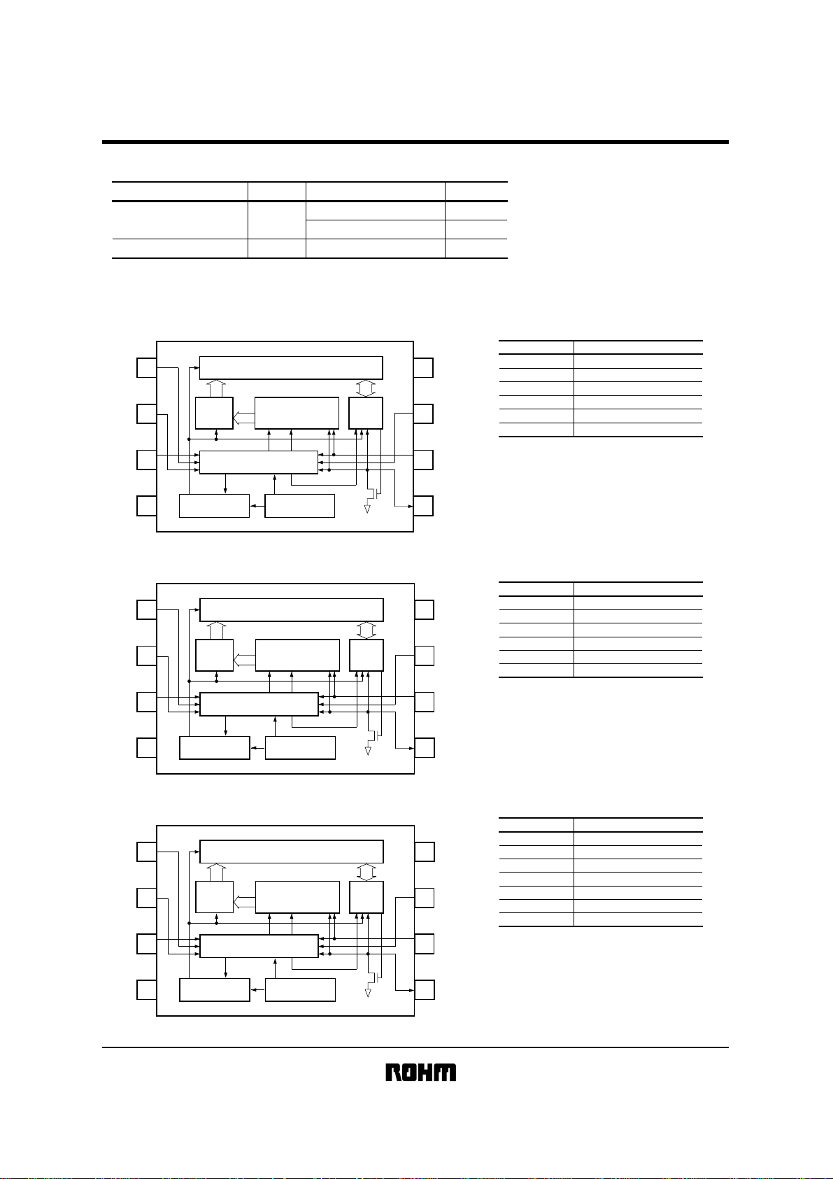
!!!!Block diagram
BR24C01A-W / AF-W / AFJ-W / AFV-W
7bits
7bits
START STOP
CONTROL LOGIC
1kbits EEPROM ARRAY
SLAVE WORD
·
ADDRESS REGISTER
VCC LEVEL DETECT
ACK
8bits
DATA
REGISTER
GND
A0
A1
A2
1
2
3
4
ADDRESS
DECODER
HIGH VOLTAGE GEN.
V
V
CC
V
!!!!Pin descriptions
Pin name Function
CC
V
8
7
WP
SCL
6
SDA
5
A0, A1, A2 Slave address setting pin
SCL Serial data clock
SDA Serial data input / output
WP Write protect pin
CC
V
Power supply
GND Ground
∗ An open drain output requires a pull-up resistor.
∗
BR24C02-W / F-W / FJ-W / FV-W
8bits
8bits
START STOP
CONTROL LOGIC
2kbits EEPROM ARRAY
ADDRESS REGISTER
GND
A0
A1
A2
1
2
3
4
ADDRESS
DECODER
HIGH VOLTAGE GEN.
BR24C04-W / F-W / FJ-W / FV-W
9bits
9bits
START STOP
CONTROL LOGIC
4kbits EEPROM ARRAY
ADDRESS REGISTER
A0
A1
A2
1
2
ADDRESS
DECODER
3
SLAVE WORD
·
VCC LEVEL DETECT
SLAVE WORD
·
ACK
ACK
8bits
DATA
REGISTER
8bits
DATA
REGISTER
Pin name Function
CC
V
8
A0, A1, A2
SCL
SDA
Slave address setting pin
Serial data clock
Serial data input / output
∗
WP Write protect pin
7
WP
CC
V
Power supply
GND Ground
∗ An open drain output requires a pull-up resistor.
SCL
6
SDA
5
Pin name
Function
A0 N.C.
CC
V
8
7
WP
A1, A2 Slave address setting pin
SCL
SDA
Serial data clock
Serial data input / output
WP Write protect pin
V
CC
Power supply
∗
GND Ground
SCL
6
∗ An open drain output requires a pull-up resistor.
GND
4
HIGH VOLTAGE GEN.
VCC LEVEL DETECT
SDA
5
BR24C01A-W / BR24C01AF-W / BR24C01AFJ-W / BR24C01AFV-W / BR24C02-W / BR24C02F-W /
Memory ICs
BR24C02FJ-W / BR24C02FV-W / BR24C04-W / BR24C04F-W / BR24C04FJ-W / BR24C04FV-W
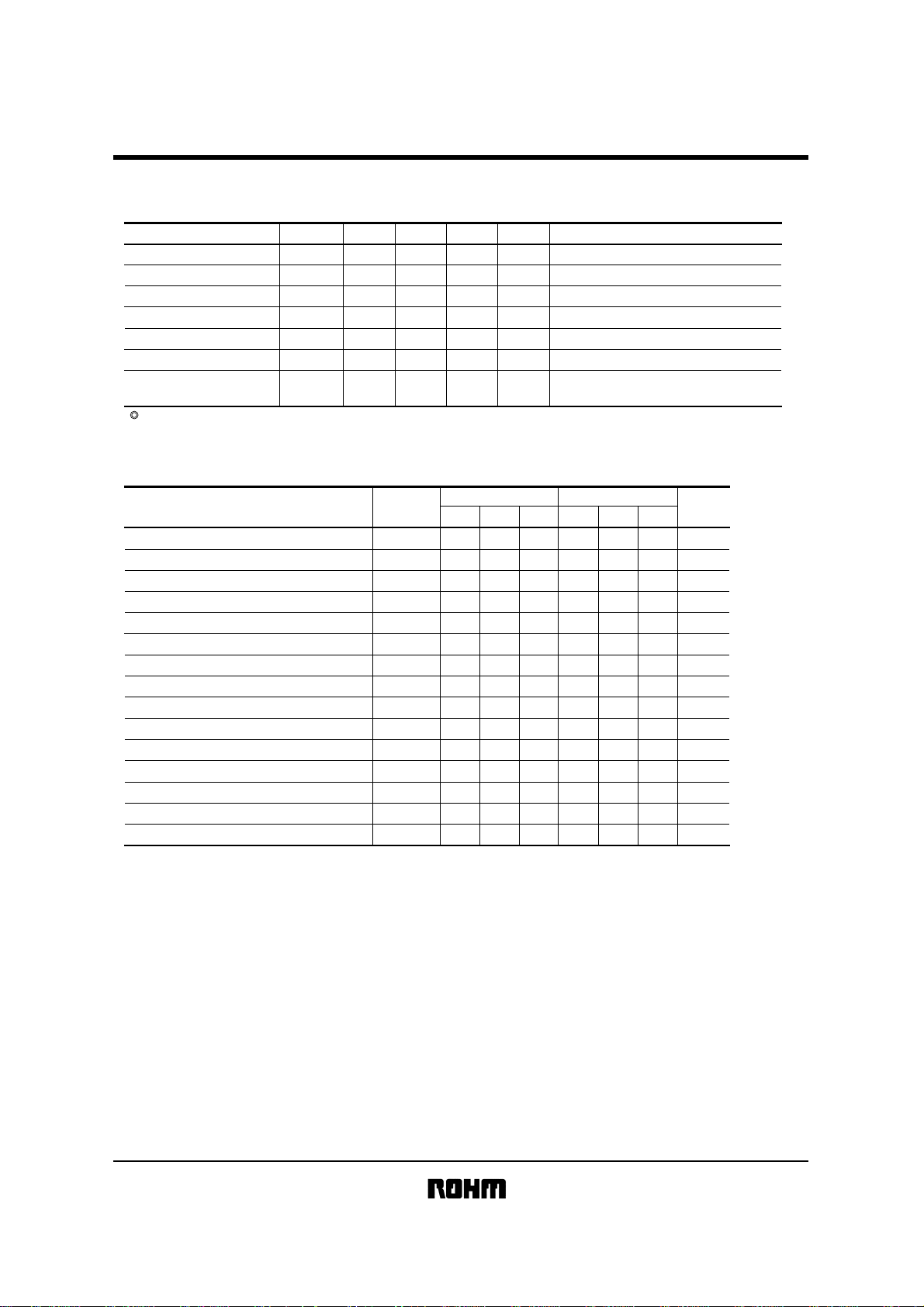
!!!!Electrical characteristics
DC characteristics (unless otherwise noted, Ta = −40 to + 85 °C, V
Parameter Symbol Min. Typ. Max. Unit Conditions
0.7V
Input high level voltage
Input low level voltage
Output low level coltage
Input leakage current I
Output leakage current I
operatingcurrent dissipation I
Standby current I
Not designed for radiation resistance.
IH
V
V
IL
V
OL
LI
LO
CC
SB
CC
−−
−−
−−
−1
−
−1 −
−
−
−
−
0.3V
= 2.7 to 5.5V)
CC
V
CC
V
0.4 V
1 µA
1 µA
2.0 mA
2.0 µA
OL
=3.0mA(SDA)
I
VIN=0V~V
V
V
V
CC
OUT
=0V~V
CC
CC
=5.5V, f
SCL
=400kHz
CC
=5.5V, SDA·SCL=V
A0, A1, A2=GND, WP=GND
Operating timing characteristics (unless otherwise noted, Ta = −40 to + 85 °C, VCC = 2.7 to 5.5V)
Parameter Symbol
SCL frequency
Data clock HIGH time
Data clock LOW time t
SDA / SCL rise time t
SDA / SCL fall time t
Start condition hold time t
Start condition setup time t
Input data hold time t
Input data setup time t
HD
SU
HD
SU
Output data delay time t
Output data hold time t
Stop condition setup time t
SU
Bus open time before start of transfer t
Noise erase valid time (SCL / SDA pins) t
f
SCL
t
HIGH
LOW
R
F
: STA
: STA
: DAT ns
: DAT ns
PD
DH
: STO
BUF
WR
t
I
Vcc=5V±10% Vcc=3V±10%
Min.
−
0.6
1.2
−
−
0.6
0.6
0
100
0.1
0.1
0.6
1.2
−
−
Typ.
−
−
−
−
−
−
−
−
−
−
−
−
−
−
−
Max.
400
−
−
0.3
0.3
−
−
−
−
0.9
−
−
−
10
0.05
Min.
−
4.0
4.7
−
−
4.0
4.7
0
250
0.2
0.2
4.7
4.7
−
−
Typ.
−
−
−
−
−
−
−
−
−
−
−
−
−
−
−
Max.
100
−
−
1.0
0.3
−
−
−
−
3.5
−
−
−
10 msInternal write cycle time
0.1
−
−
CC
Unit
kHz
µs
µs
µs
µs
µs
µs
µs
µs
µs
µs
µs

BR24C01A-W / BR24C01AF-W / BR24C01AFJ-W / BR24C01AFV-W / BR24C02-W / BR24C02F-W /
Memory ICs
!!!!Timing charts
SCL
SDA
(input)
SDA
(output)
SCL
SDA
BR24C02FJ-W / BR24C02FV-W / BR24C04-W / BR24C04F-W / BR24C04FJ-W / BR24C04FV-W
t
HIGH
t
DH
tSU : STOtHD : STA tSU : STA
tHD :
t
BUF
STA
t
t
R
tSU : DAT tHD : DAT
START BIT STOP BIT
F
t
LOW
t
PD
· Data is read on the rising edge of SCL.
· Data is output in synchronization with the falling edge of SCL.
Fig.1 Synchronized data input / output timing
SCL
ACKD0
Fig.2 Write cycle timing
WR
t
Start conditionStop condition
!!!!
Circuit operation
SDA
Write data
(n address)
(1) Start condition (recognition of start bit)
Before executing any command, when SCL is HIGH, a start condition (start bit) is required to cause SDA to fall from
HIGH to LOW. This IC is designed to constantly detect whether there is a start condition (start bit) for the SDA and
SCL line, and no commands will be executed unless this condition is satisfied.
(See Fig.1 for the synchronized data input / output timing.)
(2) Stop condition (recognition of stop bit)
To stop any command, a stop condition (stop bit) is required. A stop condition is achieved when SDA goes from
LOW to HIGH while SCL is HIGH. This enables commands to be completed.
(See Fig.1 for the synchronized data input / output timing.)
(3) Precautions concerning write commands
In the WRITE mode, the transferred data is not written to the memory unless the stop bit is executed.
 Loading...