


ROHM BD52E23G, BD52E24G, BD52E25G, BD52E26G, BD52E27G Schematic [ru]
...
Datas
Voltage Detector IC Series
Free Delay Time Setting
CMOS Voltage Detector IC Series
BD52Exxx series BD53Exxx series
●General Description
Rohm's BD52Exxx and BD53Exxx series are highly accurate, low current consumption Voltage Detector ICs with a capacitor controlled time delay. The line up includes BD52Exxx devices with N-channel open drain output and BD53Exxx devices with CMOS output. The devices are available for specific detection voltages ranging from 2.3V to 6.0V in increments of 0.1V.
●Features
Delay Time Controlled by external Capacitor
Two output types (N-channel open drain and CMOS output)
Ultra-low current consumption
Very small, lightweight and thin package
Package SSOP5 is similar to SOT-23-5(JEDEC)
●Typical Application Circuit
VDD1 |
|
|
VDD2 |
|
|
RL |
|
|
BD52Exxx |
RST |
Micro |
|
controller |
||
|
|
|
|
|
CT |
|
|
|
|
CL |
|
|
|
(Capacitor for |
|
|
|
noise filtering) |
|
|
|
|
GND |
|
Open Drain Output type |
|
|
|
BD52Exxx Series |
|
|
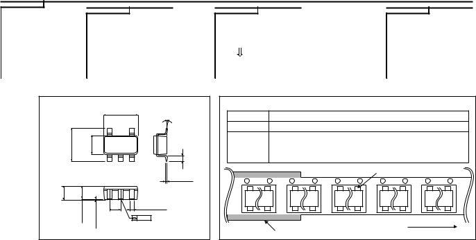
●Connection Diagram |
|
|
|
SSOP5 |
CT |
N.C. |
|
TOP VIEW |
|
||
|
|
|
|
|
|
|
|
|
|
|
|
|
Lot. No |
|
|
|
|
|
|
|
|
|
|
|
|
|
|
|
|
|
|
|
|
|
|
|
|
|
|
|
|
|
|
|
|
|
|
|
|
|
|
|
|
|
|
|
|
|
|
|
|
|
|
|
|
|
|
|
|
|
|
Marking |
|
|
|
|
|
|
|
|
|||
|
|
|
|
||||||||||
|
|
|
|
|
|
|
|
|
|
|
|||
|
|
|
|
|
|
|
|
|
|
|
|||
|
|
|
VOUT VDD GND |
||||||||||
●Pin Descriptions |
|
|
|
|
|
|
|
|
|
|
|
||
|
|
|
|
|
|
|
|
SSOP5 |
|||||
|
PIN No. |
Symbol |
|
|
|
|
|
|
|
|
|
|
Function |
|
1 |
VOUT |
|
|
|
|
|
|
|
|
|
Reset Output |
|
|
2 |
VDD |
|
|
|
|
|
|
|
Power Supply Voltage |
|||
|
3 |
GND |
|
|
|
|
|
|
|
|
|
|
GND |
|
4 |
N.C. |
|
|
|
|
|
|
|
Unconnected Terminal |
|||
|
5 |
CT |
|
|
|
|
Capacitor connection terminal for |
||||||
|
|
|
|
|
|
|
|
|
output delay time |
||||
|
|
|
|
|
|
|
|
|
|
|
|||
●Key Specifications |
|
|
Detection voltage: |
|
2.3V to 6.0V (Typ.) |
|
|
0.1V steps |
High accuracy detection voltage: |
±1.0% |
|
Ultra-low current consumption: |
0.95µA (Typ.) |
|
●Package |
|
|
SSOP5: |
2.90mm x 2.80mm x 1.25mm |
|
●Applications
Circuits using microcontrollers or logic circuits that require a reset.
VDD1 
Micro
BD53Exxx RST controller
CT
CL
(Capacitor for noise filtering)
GND 
CMOS Output type
BD53Exxx Series
○Product structure Silicon monolithic integrated circuit ○This product is not designed for protection against radioactive rays
.www.rohm.com |
|
TSZ02201-0R7R0G300080-1-2 |
|
© 2013 ROHM Co., Ltd. All rights reserved. |
1/12 |
||
22.May.2013 Rev.004 |
|||
TSZ22111 14 001 |
|
BD52Exxx series |
BD53Exxx series |
|
|
|
|
|
|
DATASHEET |
|||
|
|
|
|
|
|
|
|||||
●Ordering Information |
|
|
|
|
|
|
|
|
|
|
|
B |
D |
x |
x |
E |
x |
x |
x |
- |
T |
R |
|
|
|
|
|
|
|
|
|
|
|
|
|
|
|
|
|
|
|
|
|
|
|
|
|
|
|
|
|
|
|
|
|
|
|
|
|
Part |
Output Type |
Reset Voltage Value |
Package |
Packaging and |
||
Number |
52 |
: Open Drain |
23 : 2.3V |
|
G : SSOP5 |
forming specification |
|
53 |
: CMOS |
|
0.1V step |
|
TR : Embossed tape |
|
|
|
60 : 6.0V |
|
|
and reel |
|
|
|
|
|
|
|
SSOP5 |
|
|
|
|
|
|
|
|
|
|
|
|
|
|
|
|
|
|
+6° |
<Tape and Reel information> |
|
||
|
|
|
2.9±0.2 |
|
|
° |
Tape |
Embossed carrier tape |
|
||
|
|
|
|
|
4 |
|
−4° |
|
|||
|
|
5 |
|
4 |
|
|
|
Quantity |
3000pcs |
|
|
±0.2 |
+0.2 −0.1 |
|
|
|
|
|
|
Direction |
TR |
|
|
|
|
|
|
|
|
The direction is the 1pin of product is at the upper right when you hold |
|
||||
|
|
|
|
|
|
|
|
of feed |
|
||
2.8 |
1.6 |
|
|
|
|
|
0.2Min. |
( reel on the left hand and you pull out the tape on the right hand |
) |
||
1 |
2 |
3 |
|
|
|
||||||
|
|
|
|
|
|
|
+0.05 |
|
|
1pin |
|
1.25Max. |
|
|
|
|
0.13 −0.03 |
|
|
|
|
||
|
|
|
|
+0.05 |
|
|
|
|
|
|
|
1.1±0.05 |
|
|
|
0.42 |
|
|
|
|
|
|
|
0.05±0.05 |
|
|
−0.04 |
|
|
|
|
|
|
||
|
0.95 |
0.1 |
|
|
|
|
|
|
|
||
|
|
|
|
|
|
|
|
|
|
||
|
|
|
|
|
|
|
|
|
Direction of feed |
|
|
|
|
|
|
|
|
|
|
|
|
|
|
|
|
|
|
|
|
|
(Unit : mm) |
|
Reel |
Order quantity needs to be multiple of the minimum quantity. |
|
●Lineup
Output Type |
|
Open Drain |
|
CMOS |
|
Detection Voltage |
Marking |
|
Part Number |
Marking |
Part Number |
6.0V |
Ph |
|
BD52E60 |
Ud |
BD53E60 |
5.9V |
Pg |
|
BD52E59 |
Uc |
BD53E59 |
5.8V |
Pf |
|
BD52E58 |
Ub |
BD53E58 |
5.7V |
Pe |
|
BD52E57 |
Ua |
BD53E57 |
5.6V |
Pd |
|
BD52E56 |
Ry |
BD53E56 |
5.5V |
Pc |
|
BD52E55 |
Rr |
BD53E55 |
5.4V |
Pb |
|
BD52E54 |
Rp |
BD53E54 |
5.3V |
Pa |
|
BD52E53 |
Rn |
BD53E53 |
5.2V |
Ny |
|
BD52E52 |
Rm |
BD53E52 |
5.1V |
Nr |
|
BD52E51 |
Rk |
BD53E51 |
5.0V |
Np |
|
BD52E50 |
Rh |
BD53E50 |
4.9V |
Nn |
|
BD52E49 |
Rg |
BD53E49 |
4.8V |
Nm |
|
BD52E48 |
Rf |
BD53E48 |
4.7V |
Nk |
|
BD52E47 |
Re |
BD53E47 |
4.6V |
Nh |
|
BD52E46 |
Rd |
BD53E46 |
4.5V |
Ng |
|
BD52E45 |
Rc |
BD53E45 |
4.4V |
Nf |
|
BD52E44 |
Rb |
BD53E44 |
4.3V |
Ne |
|
BD52E43 |
Ra |
BD53E43 |
4.2V |
Nd |
|
BD52E42 |
Qy |
BD53E42 |
4.1V |
Nc |
|
BD52E41 |
Qr |
BD53E41 |
4.0V |
Nb |
|
BD52E40 |
Qp |
BD53E40 |
3.9V |
Na |
|
BD52E39 |
Qn |
BD53E39 |
3.8V |
My |
|
BD52E38 |
Qm |
BD53E38 |
3.7V |
Mr |
|
BD52E37 |
Qk |
BD53E37 |
3.6V |
Mp |
|
BD52E36 |
Qh |
BD53E36 |
3.5V |
Mn |
|
BD52E35 |
Qg |
BD53E35 |
3.4V |
Mm |
|
BD52E34 |
Qf |
BD53E34 |
3.3V |
Mk |
|
BD52E33 |
Qe |
BD53E33 |
3.2V |
Mh |
|
BD52E32 |
Qd |
BD53E32 |
3.1V |
Mg |
|
BD52E31 |
Qc |
BD53E31 |
3.0V |
Mf |
|
BD52E30 |
Qb |
BD53E30 |
2.9V |
Me |
|
BD52E29 |
Qa |
BD53E29 |
2.8V |
Md |
|
BD52E28 |
Py |
BD53E28 |
2.7V |
Mc |
|
BD52E27 |
Pr |
BD53E27 |
2.6V |
Mb |
|
BD52E26 |
Pp |
BD53E26 |
2.5V |
Ma |
|
BD52E25 |
Pn |
BD53E25 |
2.4V |
Ly |
|
BD52E24 |
Pm |
BD53E24 |
2.3V |
Lr |
|
BD52E23 |
Pk |
BD53E23 |
www.rohm.com |
|
TSZ02201-0R7R0G300080-1-2 |
|
© 2013 ROHM Co., Ltd. All rights reserved. |
2/12 |
||
22.May.2013 Rev.004 |
|||
TSZ22111 15 001 |
|
BD52Exxx series |
BD53Exxx series |
|
|
|
DATASHEET |
|||
|
|
|
|
|
||||
●Absolute maximum ratings |
|
|
|
|
|
|||
|
|
Parameter |
|
Symbol |
Limits |
Unit |
|
|
|
Power Supply Voltage |
|
VDD-GND |
-0.3 to +10 |
V |
|
||
|
Output Voltage |
|
Nch Open Drain Output |
VOUT |
GND-0.3 to +10 |
V |
|
|
|
|
CMOS Output |
|
GND-0.3 to VDD+0.3 |
|
|||
|
|
|
|
|
|
|
||
|
Output Current |
|
|
|
Io |
80 |
mA |
|
|
Power |
|
SSOP5 |
*1*2 |
Pd |
540 |
mW |
|
|
Dissipation |
|
|
|
||||
|
|
|
|
|
|
|
|
|
|
Operating Temperature |
|
Topr |
-40 to +105 |
°C |
|
||
|
Ambient Storage Temperature |
|
Tstg |
-55 to +125 |
°C |
|
||
*1 Reduced by 5.4mW/°C when used over 25°C.
*2 When mounted on ROHM standard circuit board (70mm×70mm×1.6mm, glass epoxy board).
●Electrical characteristics (Unless Otherwise Specified Ta=-40 to 105°C)
Parameter |
Symbol |
|
Condition |
|
|
Limit |
|
Unit |
|
|
|
Min. |
Typ. |
Max. |
|||||
|
|
|
|
|
|
|
|||
|
|
VDD=H L, RL=470kΩ |
*1 |
VDET(T) |
VDET(T) |
VDET(T) |
|
||
|
|
|
×0.99 |
×1.01 |
|
||||
|
|
|
|
|
|
|
|
||
|
|
|
|
Ta=+25°C |
|
2.475 |
2.5 |
2.525 |
|
|
|
VDET=2.5V |
|
Ta=-40°C to 85°C |
|
2.418 |
- |
2.584 |
|
|
|
|
|
Ta=85°C to 105°C |
|
2.404 |
- |
2.597 |
|
|
|
|
|
Ta=+25°C |
|
2.970 |
3.0 |
3.030 |
|
|
|
VDET=3.0V |
|
Ta=-40°C to 85°C |
|
2.901 |
- |
3.100 |
|
|
|
|
|
Ta=85°C to 105°C |
|
2.885 |
- |
3.117 |
|
Detection Voltage |
VDET |
|
|
Ta=+25°C |
|
3.267 |
3.3 |
3.333 |
V |
VDET=3.3V |
|
Ta=-40°C to 85°C |
|
3.191 |
- |
3.410 |
|||
|
|
|
|
|
|||||
|
|
|
|
Ta=85°C to 105°C |
|
3.173 |
- |
3.428 |
|
|
|
|
|
Ta=+25°C |
|
4.158 |
4.2 |
4.242 |
|
|
|
VDET=4.2V |
|
Ta=-40°C to 85°C |
|
4.061 |
- |
4.341 |
|
|
|
|
|
Ta=85°C to 105°C |
|
4.039 |
- |
4.364 |
|
|
|
|
|
Ta=+25°C |
|
4.752 |
4.8 |
4.848 |
|
|
|
VDET=4.8V |
|
Ta=-40°C to 85°C |
|
4.641 |
- |
4.961 |
|
|
|
|
|
Ta=85°C to 105°C |
|
4.616 |
- |
4.987 |
|
|
|
|
VDET =2.3-3.1V |
|
- |
0.80 |
2.40 |
|
|
Circuit Current when ON |
IDD1 |
VDD=VDET-0.2V |
VDET =3.2-4.2V |
|
- |
0.85 |
2.55 |
µA |
|
VDET =4.3-5.2V |
|
- |
0.90 |
2.70 |
|||||
|
|
|
|
|
|||||
|
|
|
VDET =5.3-6.0V |
|
- |
0.95 |
2.85 |
|
|
|
|
|
VDET =2.3-3.1V |
|
- |
0.75 |
2.25 |
|
|
Circuit Current when OFF |
IDD2 |
VDD=VDET+2.0V |
VDET =3.2-4.2V |
|
- |
0.80 |
2.40 |
µA |
|
VDET =4.3-5.2V |
|
- |
0.85 |
2.55 |
|||||
|
|
|
|
|
|||||
|
|
|
VDET =5.3-6.0V |
|
- |
0.90 |
2.70 |
|
|
Operating Voltage Range |
VOPL |
VOL≤0.4V, Ta=25 to 105°C, R L=470kΩ |
|
0.95 |
- |
- |
V |
||
VOL≤0.4V, Ta=-40 to 25°C, R L=470kΩ |
|
1.20 |
- |
- |
|||||
|
|
|
|
||||||
‘Low’ Output Voltage (Nch) |
VOL |
VDD=1.5V, ISINK = 0.4 mA, VDET=2.3-6.0V |
|
- |
- |
0.5 |
V |
||
VDD=2.4V, ISINK = 2.0 mA, VDET=2.7-6.0V |
|
- |
- |
0.5 |
|||||
|
|
|
|
||||||
|
|
VDD=4.8V, ISOURCE=0.7 mA, VDET(2.3V to 4.2V) |
VDD-0.5 |
- |
- |
|
|||
‘High’ Output Voltage (Pch) |
VOH |
VDD=6.0V, ISOURCE=0.9 mA, VDET(4.3V to 5.2V) |
VDD-0.5 |
- |
- |
V |
|||
|
|
VDD=8.0V, ISOURCE=1.1 mA, VDET(5.3V to 6.0V) |
VDD-0.5 |
- |
- |
|
|||
VDET (T) : Standard Detection Voltage (2.3V to 6.0V, 0.1V step)
RL: Pull-up resistor to be connected between VOUT and power supply. Design Guarantee. (Outgoing inspection is not done on all products.) *1 Guarantee is Ta=25°C.
www.rohm.com |
|
TSZ02201-0R7R0G300080-1-2 |
|
© 2013 ROHM Co., Ltd. All rights reserved. |
3/12 |
||
22.May.2013 Rev.004 |
|||
TSZ22111 15 001 |
|
BD52Exxx series |
BD53Exxx series |
|
|
|
|
DATASHEET |
|||||
|
|
|
|
|
|
|
|||||
●Electrical characteristics (Unless Otherwise Specified Ta=-40 to 105°C) - continued |
|
|
|
|
|||||||
Parameter |
|
Symbol |
|
Condition |
|
|
|
Limit |
|
Unit |
|
|
|
|
|
Min. |
Typ. |
Max. |
|
|
|||
|
|
|
|
|
|
|
|
|
|||
Leak Current when OFF |
|
Ileak |
VDD=VDS=10V |
|
*1 |
- |
- |
0.1 |
µA |
|
|
|
|
|
|
||||||||
|
|
|
VDD=VDET×1.1, V DET=2.3-2.6V, RL=470kΩ |
|
VDD |
VDD |
VDD |
|
|
||
|
|
|
|
×0.30 |
×0.40 |
×0.60 |
|
|
|||
|
|
|
|
|
|
|
|
|
|||
|
|
|
VDD=VDET×1.1, V DET=2.7-4.2V, RL=470kΩ |
|
VDD |
VDD |
VDD |
|
|
||
|
|
|
|
×0.30 |
×0.45 |
×0.60 |
|
|
|||
CT pin Threshold Voltage |
|
VCTH |
|
|
|
|
V |
|
|||
|
VDD=VDET×1.1, V DET=4.3-5.2V, RL=470kΩ |
|
VDD |
VDD |
VDD |
|
|||||
|
|
|
|
|
|
||||||
|
|
|
|
×0.35 |
×0.50 |
×0.60 |
|
|
|||
|
|
|
|
|
|
|
|
|
|||
|
|
|
VDD=VDET×1.1, V DET=5.3-6.0V, RL=470kΩ |
|
VDD |
VDD |
VDD |
|
|
||
|
|
|
|
×0.40 |
×0.50 |
×0.60 |
|
|
|||
|
|
|
|
|
|
|
|
|
|||
Output Delay Resistance |
|
RCT |
VDD=VDET×1.1 VCT=0.5V |
*1 |
5.5 |
9 |
12.5 |
MΩ |
|
||
|
|
|
|
||||||||
|
|
|
VCT=0.1V |
VDD=0.95V |
*1 |
15 |
40 |
- |
|
|
|
CT pin Output Current |
|
ICT |
|
|
µA |
|
|||||
|
VCT=0.5V |
VDD=1.5V |
|
|
150 |
240 |
- |
|
|||
|
|
|
|
|
|
|
|||||
Detection Voltage |
|
VDET/∆T |
Ta=-40°C to 105°C |
|
|
- |
±100 |
±360 |
ppm/°C |
|
|
Temperature coefficient |
|
|
|
|
|||||||
|
|
|
|
|
|
|
|
|
|
|
|
Hysteresis Voltage |
|
∆ VDET |
VDD=L H L, RL=470kΩ |
|
|
VDET |
VDET |
VDET |
V |
|
|
|
|
|
×0.03 |
×0.05 |
×0.08 |
|
|||||
|
|
|
|
|
|
|
|
|
|||
VDET (T) : Standard Detection Voltage (2.3V to 6.0V, 0.1V step)
RL: Pull-up resistor to be connected between VOUT and power supply. Design Guarantee. (Outgoing inspection is not done on all products.) *1 Guarantee is Ta=25°C.
www.rohm.com |
|
TSZ02201-0R7R0G300080-1-2 |
|
© 2013 ROHM Co., Ltd. All rights reserved. |
4/12 |
||
22.May.2013 Rev.004 |
|||
TSZ22111 15 001 |
|
BD52Exxx series BD53Exxx series |
DATASHEET |
|
|
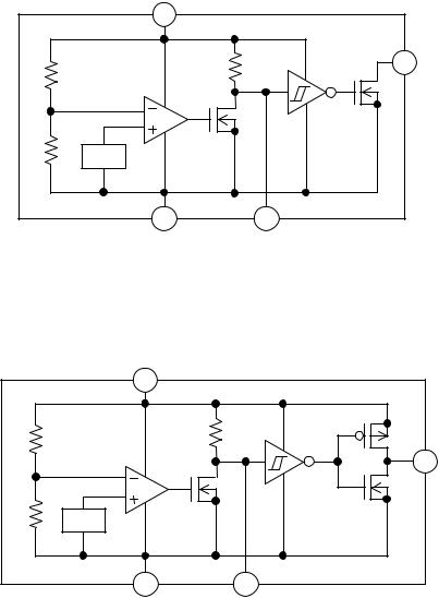
●Block Diagrams |
|
VDD |
|
|
|
|
VOUT |
Vref |
|
|
GND |
CT |
|
Figure.1 |
BD52Exxx |
Series |
VDD |
|
|
|
|
VOUT |
Vref |
|
|
GND |
|
CT |
Figure.2 |
BD53Exxx |
Series |
www.rohm.com |
|
TSZ02201-0R7R0G300080-1-2 |
|
© 2013 ROHM Co., Ltd. All rights reserved. |
5/12 |
||
22.May.2013 Rev.004 |
|||
TSZ22111 15 001 |
|
 Loading...