


ROHM BD4719G, BD4720G, BD4721G, BD4722G, BD4723G Schematic [ru]
...Datasheet
Voltage Detector IC Series
Bipolar
Voltage Detector ICs
BD47xx series
●General Description
The BD47xx series is a Voltage Detector IC, developed to prevent system errors at transient state, when the power of CPU or logic circuit switches ON/OFF or in cases of momentary shut down. These ICs consist of three terminals (power supply, GND and reset output) to detect power supply voltages and outputs reset signals of various systems. These ICs are ultra-compact and have low current consumption, making them ideal for portable products.
●Features
High accuracy detection
Low current consumption
Very small package
Open collector “L” reset output
Package SSOP5 is similar to SOT-23-5 (JEDEC)
●Key Specifications |
|
|
|
|
Detection voltage range: |
|
1.9V to 4.6V (Typ.) |
|
|
|
0.1V steps |
High accuracy detection voltage: |
±1% |
||
|
Low current consumption: |
1.6µA (Typ.) |
|
|
Operating temperature range: |
-40°C to +75°C |
|
●Package |
|
|
|
SSOP5 |
2.90mm x 2.80mm x 1.25mm |
||
●Applications
Circuits using microcontrollers or logic circuits that require a reset.
●Typical Application Circuit
|
VDD |
|
VDD |
|
|
|
RL |
|
|
BD47xx series |
VOUT |
RESET |
CPU |
|
Micro-controller |
||||
|
|
|
||
|
|
CL |
|
|
|
GND |
|
GND |
●Connection Diagram |
|
|
|
|
|
●Pin Descriptions |
|
|
|
||||||||
SSOP5 |
|
|
|
|
|
|
|
|
|
|
|
|
|
|
|
||
TOP VIEW |
|
VDD |
|
|
VOUT |
|
|
PIN No. |
|
Symbol |
Function |
|
|||||
|
|
|
|
|
|
|
|
|
|
|
|
|
|
|
|
|
|
|
|
|
|
|
|
|
|
|
|
|
|
|
1 |
|
N.C. |
Unconnected Terminal |
|
|
|
|
|
|
|
|
|
|
|
|
|
|
|
|
|
|
|
|
|
|
|
|
|
|
|
|
|
|
|
|
2 |
|
SUB |
Substrate* |
|
|
|
|
|
|
|
|
|
|
|
|
|
|
|
|
|||
|
|
|
|
|
|
|
|
|
|
|
|
|
|
|
|
|
|
|
|
|
|
|
|
|
|
|
|
|
|
|
3 |
|
GND |
GND |
|
|
|
|
|
|
|
|
|
|
|
|
|
|
|
|
|||
|
|
|
|
|
|
|
|
|
|
|
|
|
|
|
|
|
|
|
|
|
|
|
|
|
|
|
|
|
Lot. No |
|
4 |
|
VOUT |
Reset Output |
|
Marking |
|
|
|
|
|
|
|
|
|
|
|
|
|||||
|
|
|
|
|
|
|
|
|
|
|
|
|
|
|
|||
|
|
|
|
|
|
|
|
|
|
|
5 |
|
VDD |
Power Supply Voltage |
|
||
|
|
|
|
|
|
|
|
|
|
|
|
|
|||||
N.C. |
SUB GND |
|
|
|
|||||||||||||
|
|
|
|
|
|
||||||||||||
|
*Substrate Pin should be connected with GND |
||||||||||||||||
|
|
|
|
|
|
|
|
|
|
|
|
|
|||||
○Product structure Silicon monolithic integrated circuit ○This product is not designed for protection against radioactive rays |
|||||||||||||||||
.www.rohm.com |
|
|
|
|
|
|
|
|
|
|
|
|
TSZ02201-0R7R0G300020-1-2 |
||||
© 2016 ROHM Co., Ltd. All rights reserved. |
1/10 |
|
|
||||||||||||||
|
|
|
21.Jun.2016 Rev.007 |
||||||||||||||
TSZ22111 14 001 |
|
|
|
|
|
|
|
|
|
|
|
|
|
||||

BD47xx series
●Ordering Information |
|
|
|
|
|
B D 4 |
7 |
x |
x |
G - |
T R |
Part |
Reset Voltage Value |
Package |
Number |
19 : 1.9V |
G : SSOP5 |
0.1V step
46 : 4.6V |
(SOT-23-5) |
Packaging and forming specification TR : Embossed tape
and reel
●Lineup
Marking |
Detection |
Part Number |
Marking |
Detection |
Part Number |
Marking |
Detection |
Part Number |
|
Voltage |
Voltage |
Voltage |
|||||||
|
|
|
|
|
|
||||
B2 |
4.6V |
BD4746 |
BR |
3.6V |
BD4736 |
BH |
2.6V |
BD4726 |
|
B1 |
4.5V |
BD4745 |
BQ |
3.5V |
BD4735 |
BG |
2.5V |
BD4725 |
|
BZ |
4.4V |
BD4744 |
BP |
3.4V |
BD4734 |
BF |
2.4V |
BD4724 |
|
BY |
4.3V |
BD4743 |
B4 |
3.3V |
BD4733 |
BE |
2.3V |
BD4723 |
|
BX |
4.2V |
BD4742 |
BN |
3.2V |
BD4732 |
BD |
2.2V |
BD4722 |
|
BW |
4.1V |
BD4741 |
BM |
3.1V |
BD4731 |
BC |
2.1V |
BD4721 |
|
BV |
4.0V |
BD4740 |
BL |
3.0V |
BD4730 |
BB |
2.0V |
BD4720 |
|
BU |
3.9V |
BD4739 |
BK |
2.9V |
BD4729 |
BA |
1.9V |
BD4719 |
|
BT |
3.8V |
BD4738 |
BJ |
2.8V |
BD4728 |
|
|
|
|
BS |
3.7V |
BD4737 |
B3 |
2.7V |
BD4727 |
|
|
|
www.rohm.com |
|
TSZ02201-0R7R0G300020-1-2 |
|
© 2016 ROHM Co., Ltd. All rights reserved. |
2/10 |
||
21.Jun.2016 Rev.007 |
|||
TSZ22111 15 001 |
|

BD47xx series
●Absolute maximum ratings
Parameter |
Symbol |
Limit |
Unit |
Power Supply Voltage |
VDD |
-0.3 to +10 |
V |
Output Voltage |
VOUT |
-0.3 to +10 |
V |
Output Current |
Io |
60 |
mA |
Power Dissipation *1 *2 |
Pd |
540 |
mW |
Operation Temperature Range |
Topt |
-40 to +75 |
°C |
Ambient Storage Temperature |
Tstg |
-55 to +125 |
°C |
*1 Reduced by 5.4mW/°C when used over 25°C.
*2 When mounted on ROHM standard circuit board (70mm×70mm×1.6mm, glass epoxy board).
●Electrical characteristics (Unless Otherwise Specified Ta=25°C)
Parameter |
|
Symbol |
Condition |
|
Limit |
|
Unit |
|
|
Min. |
Typ. |
Max. |
|||||
|
|
|
|
|
|
|||
|
|
|
VDD=HL RL=4.7kΩ |
|
VDET (T) |
VDET(T) |
VDET(T) |
|
|
|
|
|
|
×0.99 |
|
×1.01 |
|
|
|
|
VDET=2.5V |
Ta=+25°C |
2.475 |
2.5 |
2.525 |
|
|
|
|
Ta=-40°C to 75°C |
2.418 |
- |
2.584 |
|
|
|
|
|
|
|
||||
Detection Voltage |
|
VDET |
VDET=3.0V |
Ta=+25°C |
2.970 |
3.0 |
3.030 |
V |
|
Ta=-40°C to 75°C |
2.901 |
- |
3.100 |
||||
|
|
|
|
|
||||
|
|
|
VDET=3.3V |
Ta=+25°C |
3.267 |
3.3 |
3.333 |
|
|
|
|
Ta=-40°C to 75°C |
3.191 |
- |
3.410 |
|
|
|
|
|
|
|
||||
|
|
|
VDET=4.2V |
Ta=+25°C |
4.158 |
4.2 |
4.242 |
|
|
|
|
Ta=-40°C to 75°C |
4.061 |
- |
4.341 |
|
|
|
|
|
|
|
||||
Temperature Coefficient |
|
VDET/∆T |
RL=4.7kΩTa=-20 to+75°C Designed Guarantee |
- |
±0.01 |
- |
%/°C |
|
Of Detection Voltage |
|
|||||||
|
|
|
|
|
|
|
|
|
Detection Hysteresis Voltage |
|
∆VDET |
RL=4.7kΩ, VDD=LHL |
30 |
50 |
100 |
mV |
|
Transfer Delay Time ”H” |
|
tPLH |
CL=100pF RL=4.7kΩ |
*1 |
- |
20 |
50 |
µs |
|
|
|||||||
Transfer Delay Time ”L” |
|
tPHL |
CL=100pF RL=4.7kΩ |
*2 |
- |
60 |
120 |
µs |
|
|
|||||||
Reset Output Voltage ”L” |
|
VOL |
VDD=VDET(min.)-0.05V, RL=4.7kΩ |
- |
0.1 |
0.4 |
V |
|
Circuit Current ON |
|
Icc1 |
VDD=VDET(min.)-0.05V, RL=∞ |
- |
1.5 |
3.0 |
µA |
|
Circuit Current OFF |
|
Icc2 |
VDD=VDET(typ.)/0.85V, RL=∞ |
- |
1.6 |
3.2 |
µA |
|
Operating Voltage Range |
|
VOPL |
RL=4.7kΩ VOL≤0.4V |
|
- |
0.65 |
0.85 |
V |
Output Leak Current |
|
Ileak |
VDD=VOUT=10V |
|
- |
- |
0.1 |
µA |
Reset Output Current ”L” |
|
IOL |
Vo=0.4V, VDD=VDET(min.)-0.05V |
3.0 |
15.0 |
- |
mA |
|
VDET(T):Standard Detection |
|
Voltage(1.9V |
to 4.6V, 0.1V step |
|
|
|
|
|
R :Pull-up resistor to be connected between VOUT and power supply. CL:Capacitor to be connected between VOUT and GND.
*1 tPLH:VDD=(VDET(typ.)-0.4V)(VDET(typ.)+0.4V) *2 tPHL:VDD=(VDET(typ.)+0.4V)(VDET(typ.)-0.4V)
Design Guarantee. (Outgoing inspection is not done on all products)
www.rohm.com |
|
TSZ02201-0R7R0G300020-1-2 |
|
© 2016 ROHM Co., Ltd. All rights reserved. |
3/10 |
||
21.Jun.2016 Rev.007 |
|||
TSZ22111 15 001 |
|
BD47xx series
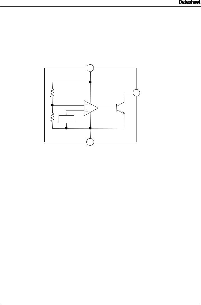
●Block Diagram
VDD |
|
|
5 |
|
4 |
|
VOUT |
Vref |
|
|
3 |
GND |
|
Fig.1 |
BD47xx series |
www.rohm.com |
|
TSZ02201-0R7R0G300020-1-2 |
|
© 2016 ROHM Co., Ltd. All rights reserved. |
4/10 |
||
21.Jun.2016 Rev.007 |
|||
TSZ22111 15 001 |
|
BD47xx series
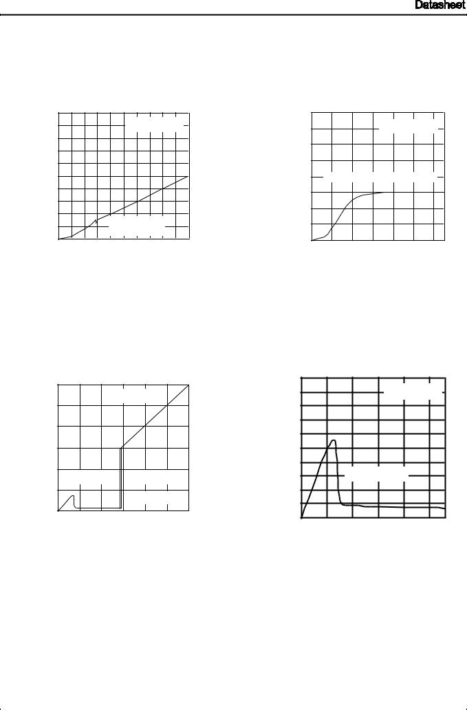
●Typical Performance Curves
|
10 |
|
|
|
|
|
|
|
|
|
|
C[μA] |
9 |
|
|
|
|
|
BD4729G |
|
|||
8 |
|
|
|
|
|
|
|
|
|
|
|
IC |
|
|
|
|
|
|
|
|
|
|
|
|
7 |
|
|
|
|
|
|
|
|
|
|
CURRENT |
|
|
|
|
|
|
|
|
|
|
|
6 |
|
|
|
|
|
|
|
|
|
|
|
5 |
|
|
|
|
|
|
|
|
|
|
|
4 |
|
|
|
|
|
|
|
|
|
|
|
CIRCUIT |
3 |
|
|
|
|
|
|
|
|
|
|
2 |
|
|
|
|
|
|
|
|
|
|
|
1 |
|
|
|
Icc1=1.34μA |
|
|
|
||||
|
|
|
|
Icc2=1.46μA |
|
|
|
||||
|
0 |
|
|
|
|
|
|
||||
|
0 |
1 |
2 |
3 |
4 |
5 |
6 |
7 |
8 |
9 |
10 |
|
|
VDD SUPPLY VOLTAGE VDD[V] |
|
||||||||
Fig.2 Circuit Current
|
6 |
|
|
|
|
|
|
|
|
|
|
|
|
|
|
T[V] |
|
|
|
BD4729G |
|
||
5 |
|
|
|
|
|
|
|
VOU |
|
|
|
|
|
|
|
|
4 |
|
|
|
|
|
|
VOLTAGE |
|
|
|
|
|
|
|
3 |
|
|
|
|
|
|
|
|
|
|
|
|
|
|
|
OUTPUT |
2 |
VDET=2.90V |
|
VDET=2.95V |
|
|
|
|
|
|
|
||||
1 |
|
|
|
VDET=50mV |
|
||
|
|
|
|
|
|||
|
|
|
|
|
|
||
|
0 |
|
|
|
|
|
|
|
0 |
1 |
2 |
3 |
4 |
5 |
6 |
|
|
VDD SUPPLY VOLTAGE VDD[V] |
|
||||
Fig.4 I/O Characteristics
[mA] |
800 |
|
|
|
|
|
|
|
|
|
|
|
|
|
|
700 |
|
|
|
BD4729G |
|||
IOL |
|
|
|
|
|
|
|
|
|
|
|
|
|
|
|
|
600 |
|
|
|
|
|
|
CURRENT |
|
|
|
|
|
|
|
500 |
|
|
|
|
|
|
|
400 |
|
IOL=12.194mA at Vo=400mV |
|||||
OUTPUT |
300 |
|
|
|
|
|
|
200 |
|
|
|
|
|
|
|
|
|
|
|
|
|
|
|
"LOW" |
100 |
|
|
|
|
|
|
0 |
|
|
|
|
|
|
|
|
0 |
5 |
10 |
15 |
20 |
25 |
30 |
|
|
OUTPUT VOLTAGE VOUT[mV] |
|||||
Fig.3 “Low” Output Current
|
1000 |
|
|
|
|
|
T[mV] |
900 |
|
|
|
BD47299G |
|
800 |
|
|
|
|
|
|
VOU |
700 |
|
|
|
|
|
|
|
|
|
|
|
|
VOLTAGE |
600 |
|
|
|
|
|
500 |
|
|
|
|
|
|
400 |
|
|
|
|
|
|
|
|
|
|
|
|
|
OUTPUT |
300 |
|
VOPL=0.675V |
|
||
|
|
|
|
|
||
200 |
|
|
|
|
|
|
100 |
|
|
|
|
|
|
|
|
|
|
|
|
|
|
0 |
|
|
|
|
|
|
0 |
0.5 |
1 |
1.5 |
2 |
2.5 |
|
|
VDD SUPPLY VOLTAGE VDD[V] |
||||
Fig.5 Operating Limit Voltage
www.rohm.com |
|
TSZ02201-0R7R0G300020-1-2 |
|
© 2016 ROHM Co., Ltd. All rights reserved. |
5/10 |
||
21.Jun.2016 Rev.007 |
|||
TSZ22111 15 001 |
|
 Loading...