


BA6780 / BA6780FP-Y
Optical disc ICs
2-channel driver for CD changers
BA6780 / BA6780FP-Y
The BA6780 and BA6780FP-Y are 2-channel driver IC for CD changers that inculdes a reversible, variable speed electronic governor and a reversible driver. On sets that have dual-rail power supplies, the BA6780 and BA6780FP-Y can be operated from just the negative supply to reduce influence on the positive power supply.
The input uses PWM control, and it is possible to directly input from a microprocessor running off the positive power supply.
zApplications
Changers for CD players and MD players.
zFeatures
1)Output voltage can be freely set using the output voltage setting pin.
2)Internal mute function if the power supply voltage drops.
3)Thermal shutdown function. (Contains hysteresis)
4)PWM input.
5)Settable reference voltage output pin.
6)Wide operating supply voltage.
zAbsolute maximum ratings (Ta = 25° C)
Parameter |
Symbol |
Limits |
Unit |
|||
|
|
|
|
|
||
Power supply voltage |
VCC |
18 |
|
V |
||
|
|
|
|
|
||
Logic input voltage |
VFIN, VRIN |
22 |
|
V |
||
|
|
|
|
|
||
Power dissipation |
BA6780 |
Pd |
1.31 1 |
W |
||
BA6780FP-Y |
1.45 2 |
|||||
|
|
|
||||
Maximum current consumption |
Imax |
1.4 3 |
A |
|||
Operating temperature |
Topr |
− 25+ |
75 |
˚C |
||
|
|
|
|
|
|
|
Storage temperature |
Tstg |
− 55+ |
150 |
˚C |
||
1 When a DIP18 package is used.Reduced by 10.48mW for each increase inTa of 1˚C over 25˚C.
2 When mounted on a PCB board (70mm 70mm, t=1.6mm glass epoxy board).
Reduced by 11.6mW for each increase in Ta of 1˚C over 25˚C.3 Should not exceed Pd or ASO values.
zRecommended operating conditions (Ta = 25° C)
|
Parameter |
Symbol |
Limits |
Unit |
|
|
|
|
|
|
|
|
|
|
Power supply voltage |
VCC |
7 16 |
|
V |
|
|
|
|
|
|
|
|
|
Input voltage for Vin |
VIN |
0 VCC / 2− |
1.0 |
V |
|
|
|
|
|
|
|
|

BA6780 / BA6780FP-Y
Optical disc ICs
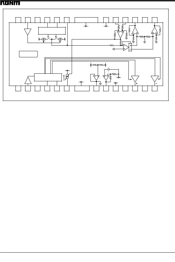
zBlock diagram and pin descriptions
BA6780 |
|
|
|
|
|
|
|
|
|
|
|
VIN2 |
FIN2 |
RIN2 |
Cτ 2 |
VEE |
FBIN− |
FBIN+ |
|
OUT2+ |
|
|
OUT2− |
18 |
17 |
16 |
15 |
14 |
13 |
12 |
|
11 |
|
|
10 |
VIN |
|
|
|
|
|
|
DRIVE BUFFER |
||||
|
GOVERNOR DRIVER |
|
VEE |
10k |
10k |
|
|||||
1/2 |
|
DETECTOR |
|
|
10k |
|
|
10k |
|||
|
|
|
|
|
|
||||||
FWD/REV CONTROLLER |
|
|
|
|
|
|
|||||
|
|
|
|
10k |
|
|
|
|
|
||
|
|
|
|
|
10k |
|
|
|
|
|
|
|
|
|
|
|
|
|
|
|
|
|
|
|
VCC |
|
VEE |
|
|
Vref |
10k |
10k |
10k |
10k |
|
|
|
|
|
3.2k |
|
|
|
|
|
||
|
|
|
|
|
10k |
|
Vref |
|
|
Vref |
|
|
|
|
|
|
|
|
Vref |
||||
|
|
|
|
|
|
|
|
||||
|
THERMAL |
|
|
|
|
Vref |
V / I |
|
|
|
|
|
|
|
|
|
|
|
|
|
|||
|
SHUT DOWN |
|
|
|
|
|
|
|
|
|
|
|
|
|
VEE |
40k |
40k |
|
|
|
|
|
|
|
|
|
|
|
|
|
|
|
|
|
|
|
|
|
|
VCC |
VEE |
20k |
|
DRIVE BUFFER |
|||
|
REVERSIBLE DRIVER |
|
|
|
|||||||
|
IOUT |
|
|
|
|
|
|
|
|
||
|
FWD/REV CONTROLLER |
|
|
17.1k VEEVCC |
|
|
|
|
|
||
|
|
|
|
|
|
|
|
|
|||
|
VIN |
|
|
Vref |
Vconst |
|
|
|
|
|
|
1 |
2 |
3 |
4 |
5 |
6 |
7 |
|
8 |
|
|
9 |
VIN1 |
FIN1 |
RIN1 |
Iout |
Vref |
Vreg |
VCC |
|
OUT1+ |
|
|
OUT1− |
Pin No. |
Pin name |
I/O |
Function |
1 |
VIN1 |
I |
Input pin for setting high output voltage for the reversible driver |
|
|
|
|
2 |
FIN1 |
I |
Input pin for forward control signal for the reversible driver |
|
|
|
|
3 |
RIN1 |
I |
Input pin for reverse control signal for the reversible driver |
|
|
|
|
4 |
Iout |
O |
Governor load current detector output (open collector 1 ) |
5 |
Vref |
O |
Internal reference voltage pin |
|
|
|
|
6 |
Vreg |
O |
4.6V constant voltage output |
|
|
|
|
7 |
VCC |
I |
Power supply (+ ) |
|
|
|
|
8 |
OUT1+ |
O |
Reversible driver output (+ ) |
|
|
|
|
9 |
OUT1− |
O |
Reversible driver output (− ) |
|
|
|
|
10 |
OUT2− |
O |
Governor output (− ) |
|
|
|
|
11 |
OUT2+ |
O |
Governor output (+ ) |
|
|
|
|
12 |
FBIN+ |
I |
Governor load current detector amplifier input (+ ) |
|
|
|
|
13 |
FBIN− |
I |
Governor load current detector amplifier input (− ) |
|
|
|
|
14 |
VEE |
I |
Power supply (− ) (connection within substrate) |
|
|
|
|
15 |
Cτ 2 |
I |
For connection of capacitor for the governor PWM filter |
|
|
|
|
16 |
RIN2 |
I |
Governor reverse control signal input |
|
|
|
|
17 |
FIN2 |
I |
Governor forward control signal input |
|
|
|
|
18 |
VIN2 |
I |
Input pin for setting high output voltage for the governor |
1 Refer to operating notes.
BA6780 / BA6780FP-Y
Optical disc ICs
BA6780FP-Y |
|
|
|
|
|
|
|
|
|
|
|
|
|
|
|
VIN2 |
|
FIN2 |
RIN2 |
Cτ 2 |
|
VEE |
FBIN− |
FBIN+ |
OUT2+ |
|
|
OUT2− |
|
25 |
24 |
23 |
22 |
21 |
20 |
|
19 |
|
18 |
17 |
16 |
|
15 |
14 |
|
VIN |
|
|
|
|
|
|
|
|
|
DRIVE BUFFER |
|
||
|
|
|
|
|
|
VEE |
VEE |
|
10k |
10k |
10k |
|||
|
1/2 |
|
GOVERNOR DRIVER |
|
|
|
|
10k |
|
|
||||
|
|
|
|
|
|
|
|
|
|
|||||
|
|
FWD/REV CONTROLLER |
|
|
|
|
|
|
|
|
|
|
||
|
|
|
|
|
|
|
|
|
|
|
|
|
||
|
|
|
|
|
|
|
|
10k |
|
10k |
|
|
|
|
|
|
VCC |
|
|
VEE |
|
|
|
|
Vref |
10k |
10k |
10k |
10k |
|
|
|
|
|
|
|
|
10k |
3.2k |
|
|
|
|
|
|
|
|
|
|
|
|
|
|
Vref |
Vref |
Vref |
|||
|
|
|
|
|
|
|
|
|
|
|
||||
|
THERMAL |
|
|
|
|
|
|
Vref |
|
|
|
|
|
|
|
|
|
|
|
|
|
|
|
|
|
|
|
|
|
|
SHUT DOWN |
|
|
|
|
|
|
|
|
|
|
|
|
|
|
|
|
|
|
|
VCC |
VEE |
|
|
|
|
|
|
|
|
|
|
|
|
VEE |
40k |
40k |
|
|
|
|
|
|
|
|
|
|
|
|
|
|
|
|
|
|
|
|
|
|
|
|
|
|
|
|
|
|
20k |
|
|
DRIVE BUFFER |
|||
|
|
REVERSIBLE DRIVER |
|
|
|
|
|
|
|
|||||
|
|
|
|
|
17.1k |
|
|
|
|
|
||||
|
|
FWD/REV CONTROLLER |
|
|
|
|
|
|
|
|
||||
|
|
|
VEE |
|
|
VEE |
|
|
|
|
|
|||
|
|
|
|
|
|
|
|
|
|
|
|
|
||
|
VIN |
|
|
IOUT |
Vref |
Vconst |
VCC |
|
|
|
|
|
||
|
|
|
|
|
|
|
|
|
|
|
||||
1 |
2 |
3 |
4 |
5 |
6 |
7 |
8 |
|
9 |
10 |
11 |
|
12 |
13 |
|
VIN1 |
|
FIN1 |
RIN1 |
Iout |
Vref |
Vreg |
|
VCC |
|
OUT1+ |
|
|
OUT1− |
Pin No. |
Pin name |
I/O |
Function |
|
|
|
|
1 |
N.C. |
− |
|
|
|
|
|
2 |
VIN1 |
I |
Input pin for setting high output voltage for the reversible driver |
|
|
|
|
3 |
N.C |
− |
|
4 |
FIN1 |
I |
Input pin for forward control signal for the reversible driver |
|
|
|
|
5 |
RIN1 |
I |
Input pin for reverse control signal for the reversible driver |
|
|
|
|
6 |
Iout |
O |
Governor load current detector output (open collector 1 ) |
7 |
Vref |
O |
Internal reference voltage pin |
|
|
|
|
8 |
Vreg |
O |
4.6V constant voltage output |
|
|
|
|
9 |
VCC |
I |
Power supply (+ ) |
|
|
|
|
10 |
N.C. |
− |
|
|
|
|
|
11 |
OUT1+ |
O |
Reversible driver output (+ ) |
|
|
|
|
12 |
N.C. |
− |
|
|
|
|
|
13 |
OUT1− |
O |
Reversible driver output (− ) |
|
|
|
|
14 |
OUT2− |
O |
Governor output (− ) |
|
|
|
|
15 |
N.C. |
− |
|
|
|
|
|
16 |
OUT2+ |
O |
Governor output (+ ) |
|
|
|
|
17 |
FB IN + |
I |
Governor load current detector amplifier input (+ ) |
18 |
FB IN − |
I |
Governor load current detector amplifier input (− ) |
|
|
|
|
19 |
VEE |
I |
Power supply (− ) (connection within substrate) |
|
|
|
|
20 |
Cτ 2 |
I |
For connection of capacitor for the governor PWM filter |
|
|
|
|
21 |
R IN 2 |
I |
Governor reverse control signal input |
|
|
|
|
22 |
F IN 2 |
I |
Governor forward control signal input |
|
|
|
|
23 |
N.C. |
− |
|
|
|
|
|
24 |
VIN2 |
I |
Input pin for setting high output voltage for the governor |
|
|
|
|
25 |
N.C. |
− |
|
1 Refer to operating notes.
BA6780 / BA6780FP-Y
Optical disc ICs
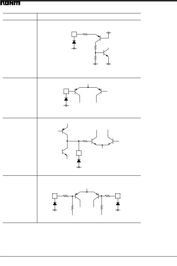
zInput / output circuits ( ( |
) :pins for BA6780FP-Y ) |
|
Pin function |
Equivalent circuit |
|
|
85k |
VCC |
|
pin 2, 3, 16, 17 |
|
|
( pin4, 5, 21, 22 ) |
|
Logic input |
24k |
|
VEE |
||
|
24k |
|
|
VEE |
VEE |
pin1, 18 ( pin2, 24 )
Voltage setting input
VEE
10k
For connection of capacitor for PWM
filter 
 pin15
pin15
( pin20 )
VEE
|
10k |
10k |
|
pin13 |
pin12 |
Load current detector |
( pin18 ) |
( pin17 ) |
|
10k |
10k |
|
|
|
|
VEE |
VEE |
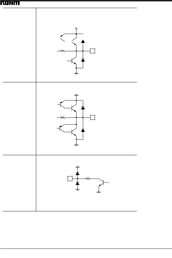
BA6780 / BA6780FP-Y
Optical disc ICs
Pin function |
Equivalent circuit |
||||||||
|
|
|
|
|
|
|
|
|
|
|
|
|
|
|
VCC |
||||
|
|
|
|
|
|
|
|
|
|
|
|
|
|
|
|
|
|
|
|
|
|
|
|
|
|
|
|
|
|
|
|
|
|
|
|
|
|
|
|
|
|
|
|
|
|
|
|
|
|
|
|
|
|
|
|
|
|
|
|
|
|
|
|
|
|
|
|
|
|
Output |
10k |
|
(reversible driver) |
||
pin8, 9 |
( pin11, 13 )
VEE
VCC
Output |
10k |
pin10, 11 |
|
(governor) |
( pin14, 16 ) |
VEE
VCC
1k
Load current detector |
pin4 |
|
( pin6 ) |
||
signal output |
||
|
||
(governor) |
|
VEE
VEE
 Loading...