


QUICK LOGIC QL12x16B-0CG84I, QL12x16B-0PF100C, QL12x16B-2PL84I, QL12x16B-2PL84M, QL12x16B-0PF100I Datasheet
...
QL12X16B
pASIC
®
1 Family
Very-High-Speed CMOS FPGA
4-13
Very High Speed
– ViaLink
metal-to-metal programmable–via
antifuse technology, allows counter speeds over 150 MHz and logic
cell delays of under 2 ns.
High Usable Density
– A 12-by-16 array of 192 logic cells
provides 2,000 usable ASIC gates (4,000 PLD gates) in 68-pin and
84-pin PLCC, 84-pin CPGA and 100-pin TQFP packages.
Low-Power, High-Output Drive
– Standby current typically 2
mA. A 16-bit counter operating at 100 MHz consumes less than 50
mA. Minimum IOL of 12 mA and IOH of 8 mA
Low-Cost, Easy-to-Use Design Tools
– Designs entered and
simulated using QuickLogic's new QuickWorks development
environment, or with third-party CAE tools including Viewlogic,
Synopsys, Mentor, Cadence and Veribest. Fast, fully automatic place
and route on PC and workstation platforms using QuickLogic
software.
=
Up to 80 prog. I/O cells, 6 Input high-drive cells, 2 Input/Clk (high-drive) cells
pASIC 1
4
pASIC
HIGHLIGHTS
QL12x16B
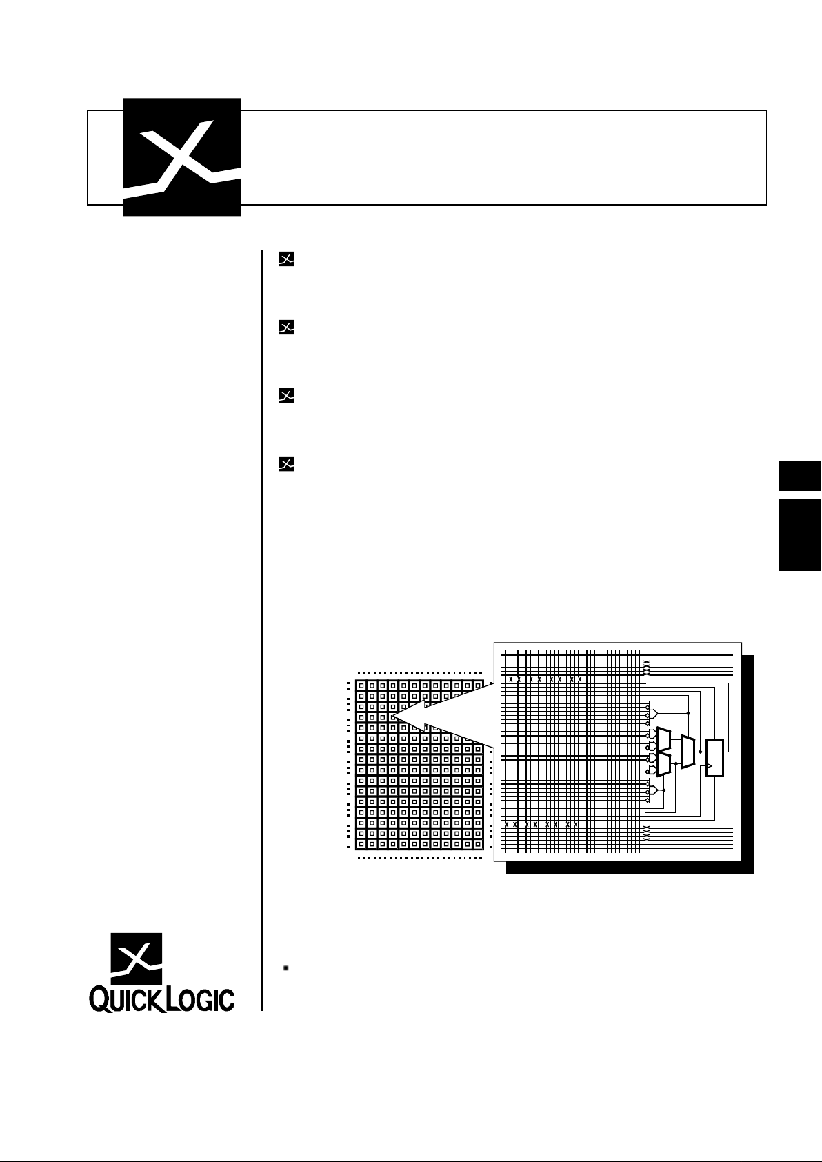
Block Diagram
Rev C
…2,000
usable ASIC gates,
88 I/O pins
192 Logic Cells
QL12x16B
4-14
The QL12x16B is a member of the pASIC 1 Family of very-high-speed
CMOS user-programmable ASIC devices. The 192 logic cell fieldprogrammable gate array (FPGA) offers 2,000 usable ASIC gates (4,000
usable PLD gates) of high-performance general-purpose logic in a wide
variety of package configurations.
Low-impedance, metal-to-metal, ViaLink interconnect technology
provides nonvolatile custom logic capable of operating above 150 MHz.
Logic cell delays under 2 ns, combined with input delays of under 1.5 ns
and output delays under 3 ns, permit high-density programmable devices
to be used with today’s fastest microprocessors and DSPs.
Designs can be entered using QuickLogic’s QuickWorks Toolkit or most
populart third-party CAE tools. QuickWorks combines Verilog/VHDL
design entry and simulation tools with device-specific place & route and
programming software. Ample on-chip routing channels allow fast, fully
automatic place and route of designs using up to 100% of the logic and
I/O cells, while maintaining fixed pin-outs.
Total of 88 I/O pins
– 80 Bidirectional Input/Output pins
– 6 Dedicated Input/High-Drive pins
– 2 Clock/Dedicated input pins with fanout-independent, low-skew
clock networks
Input + logic cell + output delays under 6 ns
Chip-to-chip operating frequencies up to 110 MHz
Internal state machine frequencies up to 150 MHz
Clock skew < 0.5 ns
Input hysteresis provides high noise immunity
Built-in scan path permits 100% factory testing of logic and I/O cells
and functional testing with Automatic Test Vector Generation
(ATVG) software after programming
Available in 68-pin and 84-pin PLCC, 84-pin CPGA and 100-pin
TQFP packages
68-pin PLCC compatible with QL8x12B
84-pin PLCC compatible with QL16x24B
100-pin TQFP compatible with QL8x12B and QL16x24B
0.65µ CMOS process with ViaLink programming technology
PRODUCT
SUMMARY
FEATURES
QL12x16B
4-15
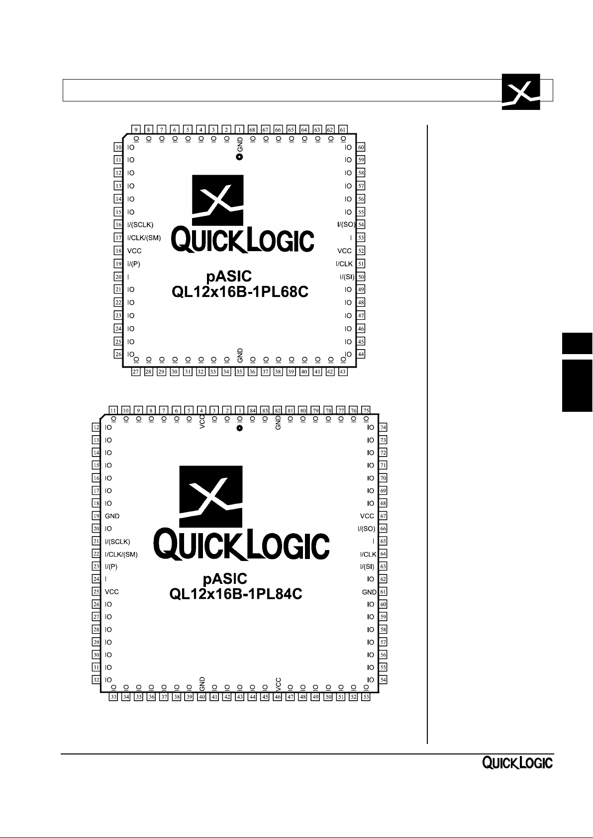
Pins identified I/SCLK, SM, SO and SI are used during scan path testing operation.
pASIC 1
4
Pinout
Diagram
68-pin PLCC
Pinout
Diagram
84-pin PLCC
 Loading...