

QUICK LOGIC QL82SD-4PT280C, QL82SD-4PT280I, QL82SD-4PT280M, QL82SD-5PB516C, QL82SD-5PB516M Datasheet
...
© 2002 QuickLogic Corporation
•
•
•
•
•
•
• • • • • •
Preliminary
1
www.quicklogic.com
Device Highlights
LVDS SERDES Basic Features
• 10 High Speed Bus LVDS Serial Links—
bandwidth up to 5 Gbps
• Eight Independent Bus LVDS serial
transceivers with operating speeds to 632
Mbps per channel
• Two Independent Bus LVDS clock serial
transceivers with operating speeds to
400 MHz per channel
• Integrated clock and data recovery (CDR)
with no external analog components
required
• CDR bypass for applications with external
clock source
• Programmable serial to parallel
configuration
• 10-bit data width—with
• clock recovery
• 4-bit, 7-bit and 8-bit data widths—
with external clock
• 1-bit asynchronous level conversion
• Fast Lock and Random (auto) Lock capable
• Lock signal feedback
• I/O support for LVTTL, LVCMOS, PCI,
GTL+, SSTL2, SSTL3, LVDS, LVPECL
• Low Power/Independent power-down
mode for each SERDES channel
• IEEE1149.1 JTAG Support &
boundary scan
• Operation over PCB or backplane traces, or
across twisted pair cabling up to 25 m
• Point-to-Point, Multi-Point, and Multi-Drop
Support
• Pre-Emphasis Control on each LVDS
Channel Link
Extended Features
The following can be implemented into the
programmable logic:
• UTOPIA Level 2, 16-bit wide System
interface (up to 50 MHz) with parity support
for ATM applications
• UTOPIA Level 3 compatible 8-bit wide
system Interface (up to 100 MHz) with parity
support for ATM applications
• CSIX-L1 32-bit switch fabric interface (up to
100 MHz)
• Supports Generic 8,16,32-bit
microprocessor bus interface for
configuration, control and status monitoring
• Supports Generic 32, 64-bit peripheral bus
interface for bridging functions
Flexible Programmable Logic
• 2,016 Programmable Logic Cells
• 536 K System Gates
• Muxed architecture; non-volatile technology
• Completely customizable for any digital
application
Dual Port SRAM Blocks
• 36 Dual Port SRAM Blocks
• Configurable array sizes (by 2, 4, 9, 18)
• < 3 ns access times, FIFO capable of over
300 MHz
• Configurable as RAM or FIFO
QL82SD Device Data Sheet
www.quicklogic.com
© 2002 QuickLogic Corporation
•
•
•
•
•
•
QL82SD Device Data Sheet Rev C
Preliminary
2
Programmable I/O
• Up to 252 Programmable I/O pins
• High performance Enhanced I/O (EIO): Less than 3 ns Tco
• Programmable Slew Rate Control
• Programmable I/O Standards
• LVTTL, LVCMOS, PCI, GTL+, SSTL2, and SSTL3, LVDS, LVPECL
• Four Independent I/O Banks
• Three Register Configuration: Input, Output, OE
Embedded Computational Unit (ECU) Blocks
• Integrated multiply, add, and accumulate function
• 18 distributed MAC blocks
• 8 × 8 multiply (sign & unsigned)
• 16-bit carry add
Advanced Clock Network
• Nine Global Clock Networks consisting of:
• one dedicated
• eight programmable
• Eight I/O (high drive) networks: two I/Os per bank
• Ten Quad-Net Networks—five per quadrant
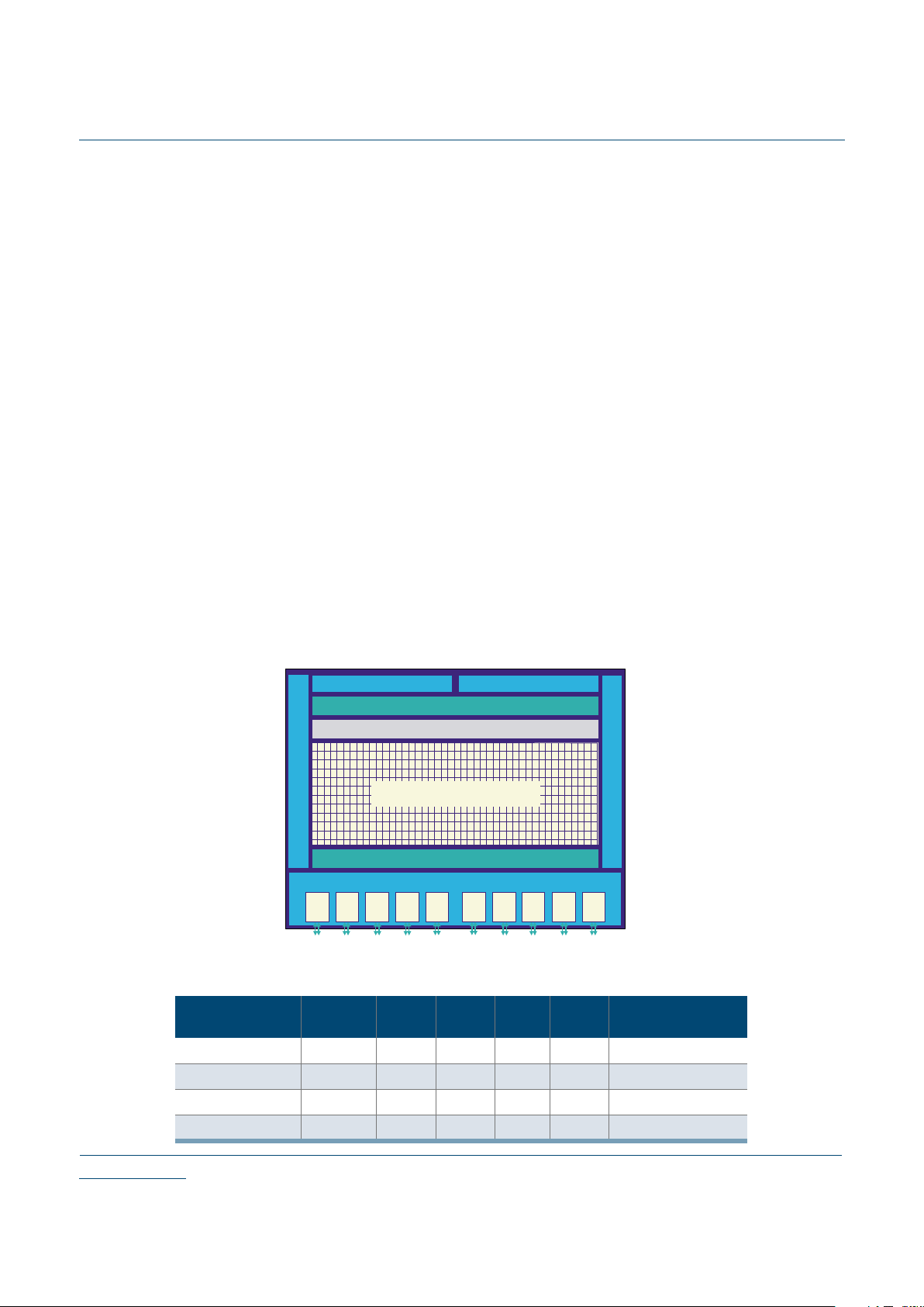
Figure 1: QL82SD Device Block Diagram
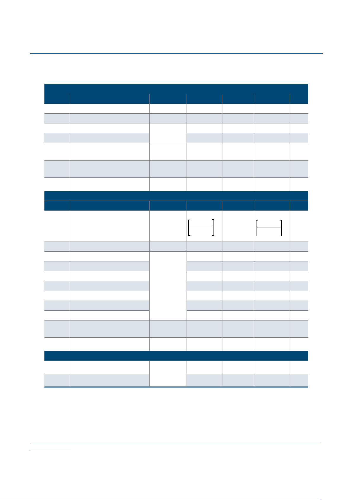
Table 1: QL82SD Device Table
Customer Part #
SERDES
Data
LV DS
Clocks
SRAM
Blocks
Logic
Cells
ECU
Blocks
Programmable I/O
QL82SD-PQ208 4 2 36 2016 18 75
QL82SD-PT280 8 2 36 2016 18 121
QL82SD-PS484 8 2 36 2016 18 209
QL82SD-PB516 8 2 36 2016 18 252
RAM Blocks
Embedded Computational Units (ECUs)
RAM Blocks
IO Block IO Block
IO Block
2016 Logic Cells
CLKB
CH7
CH6
CH5
CH4
CH3
CH2
CH1
CH0
CLKA
LVDS/SERDES IO Block
IO Block
© 2002 QuickLogic Corporation
•
•
•
•
•
•
QL82SD Device Data Sheet Rev C
Preliminary
3
www.quicklogic.com
General Description
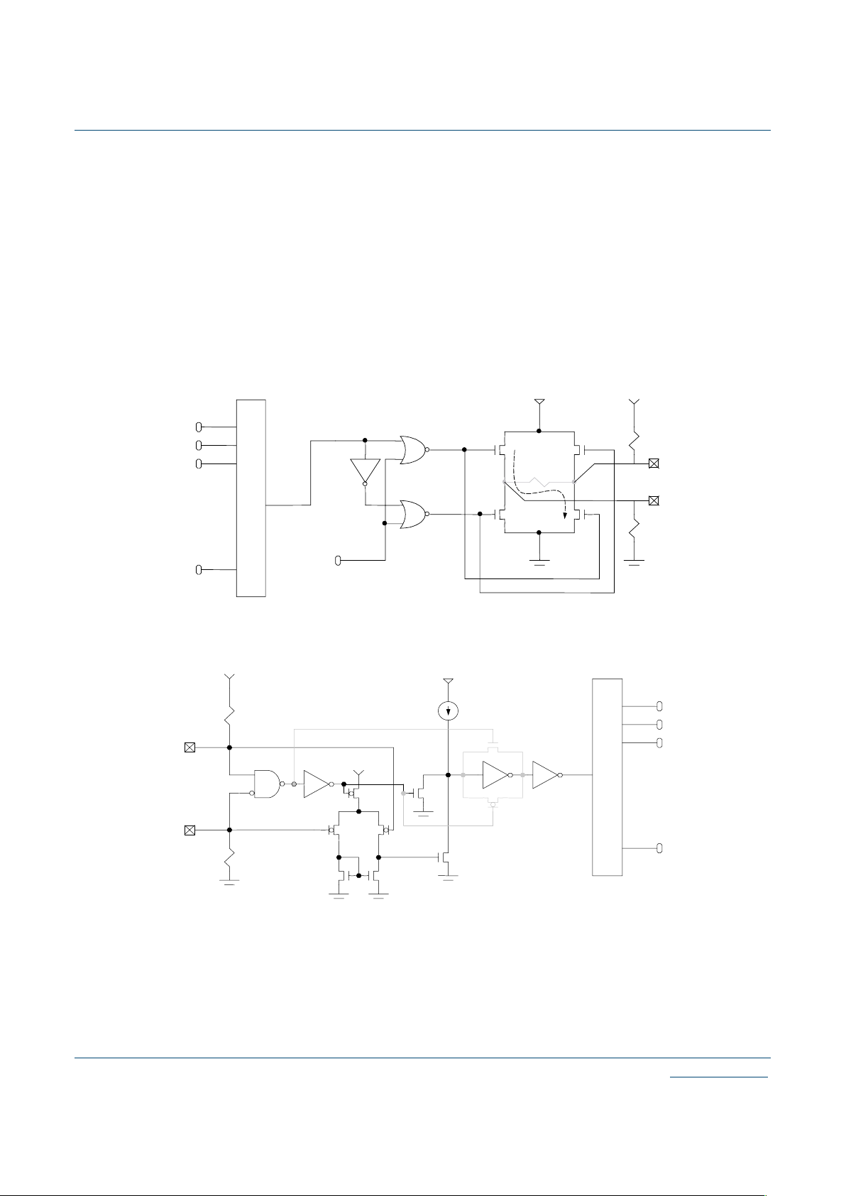
LVDS SERDES Transmitter and Receiver
A QuickSD LVDS SERDES device in serializer mode takes a parallel data bus and a separate
clock and converts them into a serial data stream. In deserializer mode, it takes a serial data
stream and converts it to a configurable bit wide parallel data bus and separate clock. The
reduced number of I/O board traces and cable connectors saves on cost and significantly
simplifies design. Skew and timing issues are significantly reduced and performance is
enhanced.
Figure 2 and Figure 3 illustrate the block diagrams of the QuickSD device
transmitter and receiver.
Figure 2: LVDS SERDES Transmitter Block Diagram
Figure 3: LVDS SERDES Receiver Block Diagram
RL = 2 7
Ω
- 100ΩVo +
Vo -
IL = 8-12 mA
Do +
Do -
300k
300k
/E nabl e
Parallel to Serial
.
.
.
.
txd [9:0]
TTL_Din
Din +
Din -
300k W
300k W
VCM = 0.2 V - 2.2 V
Serial to Parallel
.
.
.
.
FPGA
rxd [9:0]

www.quicklogic.com
© 2002 QuickLogic Corporation
•
•
•
•
•
•
QL82SD Device Data Sheet Rev C
Preliminary
4
LVDS SERDES Applications
The QuickSD device is designed to address the need for high-speed serial communications.
It maintains the features of standard discrete SERDES devices, but integrates these features
with customizable logic to allow for the highest degree of flexibility, performance, and
integration at the lowest cost. The QuickSD device is designed to support both transmit and
receive requirements in a single chip. The device can support multiple channels in a variety
of modes (with or without clock recovery,) a variety of translation widths (1:1 to 1:10), as
well as a range of frequencies. These capabilities make this device ideal in applications where
the performance is critical and customization is required.
The QuickSD device targets three applications: on-board, board-to-board (via common
backplane), and box-to-box (via common cable).
Software Support
The turnkey QuickWorks package from QuickLogic provides the most complete ESP and
FPGA software solution from design entry to logic synthesis, to place and route, and to
simulation. The package provides a solution for designers who use third-party tools from
Cadence, Mentor, OrCAD, Synopsys, Viewlogic, Veribest and other third-party tools for
design entry, synthesis, or simulation. A power calculator is also provided for SERDES power
consumption.
To speed up the QuickSD design process, QuickLogic includes a SERDES Wizard in its
QuickWorks package. This wizard simplifies the process of configuring the multi-channel
SERDES core into each of its modes. For details on the SERDES Wizard, please refer to "The
QL82SD Quickstart Design Guide". To find this guide go to the QuickSD device
documentation Web page at
http://www.quicklogic.com/home.asp?PageID=315&sMenuID=199#Order.
Process Data
QuickSD is fabricated on a 0.25 µ, five-layer metal CMOS process. The core voltage is
2.5 Volt V
CC
supply and 3.3 V tolerant I/O with the addition of 3.3 Volt V
CCIO
. QuickSD is
available in commercial and industrial temperature grades.
© 2002 QuickLogic Corporation
•
•
•
•
•
•
QL82SD Device Data Sheet Rev C
Preliminary
5
www.quicklogic.com
Ordering Information
Maximum Ratings and Operating Range
Table 2: Absolute Maximum Electrical Ratings
VCC Voltage -0.3 V to 4 V
Bus LVDS Driver
Output Voltage
-0.3 V to +2.8 V
LVCMOS/LVTTL
Input Voltage
-0.3 V to (V
CC
+ 0.3 V)
Bus LVDS Output Short
Circuit Duration
10 mS
LVCMOS/LVTTL
Output Voltage
-0.3 V to (V
CC
+ 0.3 V) ESD Rating HBM 2 kV
Bus LVDS Receiver
Input Voltage
-0.3 V to +2.8 V
Table 3: Absolute Maximum Thermal Ratings
Junction Temperature +150°C
Lead Temperature
(Soldering, 4 seconds)
+260°C
Storage Temperature -65°C to +150°C
Thermal and Power
Dissipation
Characteristics
See the following table
Table 4: Thermal and Power Dissipation Characteristics
Package 0ja (*C/W vs. Airflow 0jc (*C/W)
Estimated Maximum
Power Dissipation (W)
0.0 0.5 1.0 2.0
PQ208 26.0 24.5 23.0 22.0 11.0 1.65
QL 82SD - 4 PB516 C
QuickLogic device
QuickSD device
part number
Speed Grade
4 = Quick
5 = Fast
6 = Faste r
7 = Faste st
Package Code
PQ208 = 208-pin FPBGA
PT280 = 280-pin BGA (1.0mm)
PS484 = 484-pin BGA (1.0mm)
PB516 = 516-pin BGA (1.27mm)
Operating Range
C = Commercial
I = Industrial
M = Military
www.quicklogic.com
© 2002 QuickLogic Corporation
•
•
•
•
•
•
QL82SD Device Data Sheet Rev C
Preliminary
6
Electrical Specifications - LVDS SERDES
LVDS SERDES Transceiver Capability (Speed)
General Test Conditions
All tests are done for the 484-pin BGA package (1.00 mm pitch). The tests are set up so
that an LVDS SERDES channel of a QL82SD transmits, and the other LVDS SERDES
channel of the same device (or another QL82SD device) receives. All results are given as
worst cases over commercial temperature, VCC, and process, with PLLVCC = 2.5 V unless
otherwise specified.
If the QL82SD device is used only for transmit or receive, but not both simultaneously, the
performance can be significantly better, and, in many cases, exceeds 1 Gb/s per channel.
NOTE:
All data are in Mb/s. Low/High frequencey refers to internal SERDES PLL lock
range (see
Table 29 on page 31 for more information).
PT280 18.5 17.0 15.5 14.0 7.0 2.24
PS484 28.0 26.0 25.0 23.0 9.0 2.42
PB516 20.0 19.0 17.5 16.0 7.0 2.51
Table 5: Operating Ranges
Symbol Parameter Industrial Commercial Unit
Min Max Min Max
Vcc Supply Voltage 2.3 2.7 2.3 2.7 V
Vccio I/O Input Tolerance Voltage 2.3 3.6 2.3 3.6 V
T
A
Ambient Temperature -40 85 0 70 °C
K Delay Factor
-4 Speed Grade 0.43 2.16 0.47 2.11 n/a
-5 Speed Grade 0.43 1.80 0.46 1.76 n/a
-6 Speed Grade 0.43 1.26 0.46 1.23 n/a
-7 Speed Grade 0.43 1.14 0.46 1.11 n/a
Table 4: Thermal and Power Dissipation Characteristics
Package 0ja (*C/W vs. Airflow 0jc (*C/W)
Estimated Maximum
Power Dissipation (W)
0.0 0.5 1.0 2.0

© 2002 QuickLogic Corporation
•
•
•
•
•
•
QL82SD Device Data Sheet Rev C
Preliminary
7
www.quicklogic.com
Cable - Normal Operation
NOTE:
Test Conditions: Up to 3-meter Category 5 Cable without any compensation.
Cable - High Speed Operation
NOTE:
Test Conditions: Up to 9" Category 5 Cable, and reference design in the
programmable fabric portion of the device for internal skew compensation for channel link
modes.
Backplane - Normal Operation
NOTE:
Test Conditions: Up to 18" point-to-point backplane without any compensation.
Table 6: Cable - Normal
Low Frequency High Frequency
Modes Min Max Min Max
10:1 Mode Not Available 250 350
8:1 112 360 224 368
7:1 112 322 224 364
4:1 112 348 224 304
Table 7: Cable - High Speed Operation
Low Frequency High Frequency
Modes Min Max Min Max
10:1 Mode Not Available 250 350
8:1 112 480 224 552
7:1 112 462 224 504
4:1 112 456 224 500
Table 8: Backplane - Normal Operation
Low Frequency High Frequency
Modes Min Max Min Max
10:1 Mode Not Available 250 350
8:1 112 320 224 376
7:1 112 315 224 385
4:1 112 384 224 384
www.quicklogic.com
© 2002 QuickLogic Corporation
•
•
•
•
•
•
QL82SD Device Data Sheet Rev C
Preliminary
8
Backplane - High Speed Operation
NOTE:
Test Conditions: Up to 18" point-to-point backplane, and reference design in the
programmable fabric portion of the device for internal skew compensation for channel link
modes.
1:1 Mode (Asynchronous Level Conversion)
Up to 9" cable: 0 to 500 Mbps
Up to 18" point-to-point backplane: 0 to 700 Mbps
All numbers are for LVDS channel performance only, and do not include the programmable
fabric’s ability to support high data rates.
Table 9: Backplane - High Speed Operation
Low Frequency High Frequency
Modes Min Max Min Max
10:1 Mode Not Available 250 350
8:1 112 632 224 632
7:1 112 630 224 630
4:1 112 628 224 628
© 2002 QuickLogic Corporation
•
•
•
•
•
•
QL82SD Device Data Sheet Rev C
Preliminary
9
www.quicklogic.com
Bus LVDS DC Specifications
Over the operating range, RxVcc = 3.0 V to 3.6 V.
NOTE:
Apply to pad_ChX_p/n, pad_ClkX_p/n
Figure 4: Output Differential Voltage
Table 10: Serializer / Transmitter
Symbol Parameter Conditions Min Typ Max Units
V
OD
Output Differential Voltage,
pad_ChX_p - Pad_ChX_n
Figure 4
Figure 5
R
L
= 27Ω
240 325 420 mV
V
OS
Offset Voltage 0.90 1.10 1.30 V
I
OS
Output Short Circuit Current
D
O
= 0 V,
D
IN
+ H,
EN + OE + V
CC
20 25 35 mA
I
OZ
Tri-State Output Current
DO = 0 V/VCC,
EN = 0
-25 ±10 25 µA
I
OX
Power-Off Output Current
V
CC
- 0 V,
D
O
= 0 V/V
CC
-25 ±10 25 µA
Table 11: Deserializer / Receiver
Symbol Parameter Conditions Min Typ Max Units
V
TH
Differential Threshold High Voltage
Figure 6
V
CM
= 1.1 V
n/a 35 50 mV
V
TL
Differential Threshold Low Voltage -50 -35 n/a mV
I
IN
Input Current
V
IN
= 0 V,
V
CC
= 0 V / 3.6 V
-25±825µA
VIN = 2.4 V,
V
CC
= 0 V / 3.6 V
-25 ±8 25 µA
D out +
D out -
www.quicklogic.com
© 2002 QuickLogic Corporation
•
•
•
•
•
•
QL82SD Device Data Sheet Rev C
Preliminary
10
Figure 5: Output Differential Voltage for Different Loads
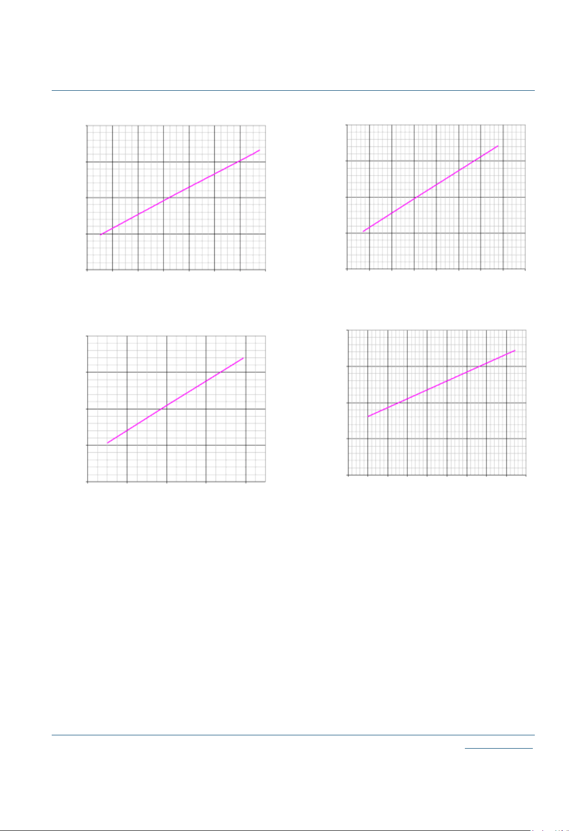
Figure 6: Differential Threshold Voltages
82SD BLVDS output Vod vs Iod
0.00
0.10
0.20
0.30
0.40
0.50
0.60
0.70
0.80
0.90
1.00
8 9 10 11 12 13
Iod ( m A )
Vod ( v )
100
Ω
60
Ω
27
Ω
40
Ω
80
Ω
VCM
VTH/ VTL

© 2002 QuickLogic Corporation
•
•
•
•
•
•
QL82SD Device Data Sheet Rev C
Preliminary
11
www.quicklogic.com
Supply Current per Channel
NOTE:
More accurate supply current/power consumption numbers specific to your
application should be calculated using the power calculator supplied with QuickLogic’s
QuickWorks software package.
Table 12: Serializer / Transmitter
Symbol Parameter Conditions Min Typ Max Units
I
CCT
Serializer Supply Current CL =10 pF
Figure 7 1:1 Mode Figure 7 mA
Figure 8 4:1 Mode Figure 8 mA
Figure 9 7:1 Mode Figure 9 mA
Figure 12 8:1 Mode Figure 12 mA
Figure 11
10:1 Mode
Data/Clock
Figure 11 mA
I
CCTX
Serializer Supply Current
Powerdown
EN = 0 1 10 µA
Table 13: Deserializer / Receiver
Symbol Parameter Conditions Min Typ Max Units
I
CCR
Serializer Supply Current CL = 10 pF
Figure 13 1:1 Mode Figure 13 mA
Figure 14 4:1 Mode Figure 14 mA
Figure 15 7:1 Mode Figure 15 mA
Figure 13 8:1 Mode Figure 13 mA
Figure 14
10:1 Mode
Data/Clock
Figure 14 mA
I
CCRX
Serializer Supply Current
Powerdown
EN = 0 1 10 µA
www.quicklogic.com
© 2002 QuickLogic Corporation
•
•
•
•
•
•
QL82SD Device Data Sheet Rev C
Preliminary
12
Figure 7: Data/Clock Channel, 1:1 Transmit Mode
Figure 8: Data/Clock Channel, 4:1 Transmit Mode
Figure 9: Data/Clock Channel, 7:1 Transmit Mode
Figure 10: Data/Clock Channel, 8:1 Transmit Mode
Figure 11: Data/Clock Channel,10:1 Transmit Mode
Figure 12: Data/Clock Channel, 1:1 Receive Mode
S
upply Current at VccTx = 2.5
V
ICCT (mA)
Clock Frequency(MHz)
0
9
10
11
12
13
0 100 200 300 400 500 600 700
Rt=100ohm
Rt= 27ohm
Supply Current at VccTx = 2.5 V
ICCT (mA)
Clock Frequency(MHz)
10
15
20
20 40 60 80 100 120 140 160
Rt=100ohm
Rt= 27ohm
Supply Current at VccTx = 2.5V
ICCT (mA)
Clock Frequency(MHz)
10
10 30 50 70 90
Rt=100ohm
Rt= 27ohm
15
20
25
Supply Current at VccTx = 2.5 V
ICCT (mA)
10
20 40 60
15
20
25
Rt=100ohm
Rt= 27ohm
Clock Frequency(MHz)
Supply Current at VCCRX = 3.3 V V
CC
= 2.5 V
ICCR (mA)
Clock Frequency (MHz)
2
0 100 200 300 400 500 600 700
4
6
8
10
12
14
16
18
20
S
upply Current at VccTx = 2.5
V
ICCT (mA)
Clock Frequency(MHz)
10
10 30 50 70
Rt=100ohm
Rt= 27ohm
15
20
25
© 2002 QuickLogic Corporation
•
•
•
•
•
•
QL82SD Device Data Sheet Rev C
Preliminary
13
www.quicklogic.com
Figure 13: Data/Clock Channel, 4:1 Receive Mode
Figure 14: Data/Clock Channel, 7:1 Receive Mode
Figure 15: Data/Clock Channel, 8:1 Receive Mode
Figure 16: Data/Clock Channel, 10:1 Receive Mode
ICCR (mA)
Clock Frequency (MHz)
5
20 40 60 80 100 120 140 160
15
20
25
Supply Current at V
CCRX
= 3.3 V, V
CC
= 2.5 V
10
ICCR (mA)
Clock Frequency (MHz)
S
upply Current at VCCRX = 3.3 V, V
CC
= 2.5 V
0
10 30 50 70 90
20
10
5
15
ICCR (mA)
Clock Frequency (MHz)
10 20 30 40 50 60 70 80 90
5
S
upply Current at
VCCR
X
= 3.3 V,
V
CC
= 2.5
V
20
15
10
0
ICCR (mA)
Clock Frequency (MHz)
S
upply Current at
VCCR
X
= 3.3 V,
V
CC
= 2.5
V
0
10
15
20
5
20 25 30 35 40 45 50 55 60 70
www.quicklogic.com
© 2002 QuickLogic Corporation
•
•
•
•
•
•
QL82SD Device Data Sheet Rev C
Preliminary
14
SERDES Timing Requirements
NOTE:
Both Table 14 and Tabl e 15 refer to CDR (10:1) Mode for ChX_txclk and
Channel Link (8:1, 7:1, 4:1) Mode for ClkX_txclk
Figure 17: Serializer Transmit Clock / Deserializer Reference Clock Transition Times
Table 14: Serializer / Transmitter Transmit Clock
Symbol Parameter Conditions Min Ty p Max Units
t
TCP
Transmit Clock Period
Mode
Dependent
n/a T n/a nS
t
TDC
Transmit Clock Duty Cycle 45 50 55 %
t
CLKT
Transmit Clock Input Transition Time Figure 17 1 n/a n/a V/nS
t
JIT
Transmit Clock Input Jitter n/a n/a 150.0
pS
(RMS)
Table 15: Deserializer / Receiver Transmit Clock
Symbol Parameter Conditions Min Ty p Max Units
t
RFCP
Reference Clock Period
Mode
Dependent
n/a T n/a nS
t
RFDC
Reference Clock Duty Cycle 40 50 60 %
t
RFCP/tTCP
Ratio of Reference Clock to
Transmit Clock
0.4 0.5 0.6 n/a
t
RFTT
Reference Clock Transition Time Figure 17 1 n/a n/a V/nS
90%
90%
10%
10%
txclk
tclkT/tRFTT tclkT/tRFTT
© 2002 QuickLogic Corporation
•
•
•
•
•
•
QL82SD Device Data Sheet Rev C
Preliminary
15
www.quicklogic.com
SERDES Switching Characteristics - Serializer/Transmitter]
Table 16: Serializer/Transmitter Switching Characteristics
CDR (10:1) Mode
Symbol Parameter Conditions Min Typ Max Units
t
HZD
pad_ChX_p/n High to Tri-State Delay
Figure 18
1.9 2.2 2.5 nS
t
LZD
pad_ChX_p/n Low to Tri-State Delay 1.9 2.0 2.2 nS
t
ZHD
pad_ChX_p/n Tri-State to High Delay 1.9 2.4 3.0 nS
t
ZLD
pad_ChX_p/n Tri-State to Low Delay 2.0 2.3 2.8 nS
t
DIS
ChX_txd[9:0] Setup to ChX_txclk
Figure 19
2.6 3.2 nS
t
DIH
ChX_txd[9:0] Hold from ChX_txclk 2.1 2.7 nS
t
PLD
Serializer PLL Lock Time Figure 20 90 uS
Channel Link (8:1, 7:1, 4:1) Mode
Symbol Parameter Conditions Min Typ Max Units
t
HZD
pad_ChX_p/n High to Tri-State Delay
Figure 18
1.9 2.2 2.5 nS
t
LZD
pad_ChX_p/n Low to Tri-State Delay 1.9 2.0 2.2 nS
t
ZHD
pad_ChX_p/n Tri-State to High Delay 1.9 2.4 3.0 nS
t
ZLD
pad_ChX_p/n Tri-State to Low Delay 2.0 2.3 2.8 nS
t
DIS
ChX_txd[N-1:0] Setup to ChX_txclk
Figure 21
2.6 3.2 nS
t
DIH
ChX_txd[N-1:0] Hold from ChX_txclk 2.1 2.7 nS
t
SD
Serializer Delay 1.7 nS
t
SCP
Serial Transmit Clock Period T/mode nS
t
TXD[N-1]
Transmitter Output Pulse Position for
Bit [N-1]
[N-1] x t
SCP
+ 1.1 [N-1] x t
SCP
+ 1.5 nS
t
PLD
Serializer PLL Lock Time Figure 20 90 uS
Asynchronous Level Conversion (1:1) Mode
t
HZD
pad_ChX_p/n High to Tri-State Delay
Figure 18
1.9 2.2 2.5 nS
t
LZD
pad_ChX_p/n Low to Tri-State Delay 1.9 2.0 2.2 nS
t
ZHD
pad_ChX_p/n Tri-State to High Delay 1.9 2.4 3.0 nS
t
ZLD
pad_ChX_p/n Tri-State to Low Delay 2.0 2.3 2.8 nS
t
ASD
Asynchronous Serializer Delay -
Data Channel
Figure 22
1.8 nS
t
ASC
Asynchronous Serializer Delay -
Channel Clock
1.7 nS
www.quicklogic.com
© 2002 QuickLogic Corporation
•
•
•
•
•
•
QL82SD Device Data Sheet Rev C
Preliminary
16
Figure 18: Serializer Delays to Tri-State
Figure 19: 10:1 Mode Serializer Transmit with Embedded Clock
Figure 20: Serializer PLL Times
3V
0V
V
V
0H
0L
EN
Pad_p/n
t
LZD
t
HZD
t
ZHD
t
ZLD
50%
1.1V
50%
50%
50%
1.5V1.5V
1.1V
Ch0_txclk
Ch0_txd[9:0]
A
B
C
D
E
DIS
DIH
t
t
F
Pad_Ch0_p/n
t
ZHD
or
t
ZLD
0.8V
t
HZD
or
t
LZD
TRI-STATE
Output Active
TRI-STATE
txclk
Pad_p/n
ENABLE
2.0V

© 2002 QuickLogic Corporation
•
•
•
•
•
•
QL82SD Device Data Sheet Rev C
Preliminary
17
www.quicklogic.com
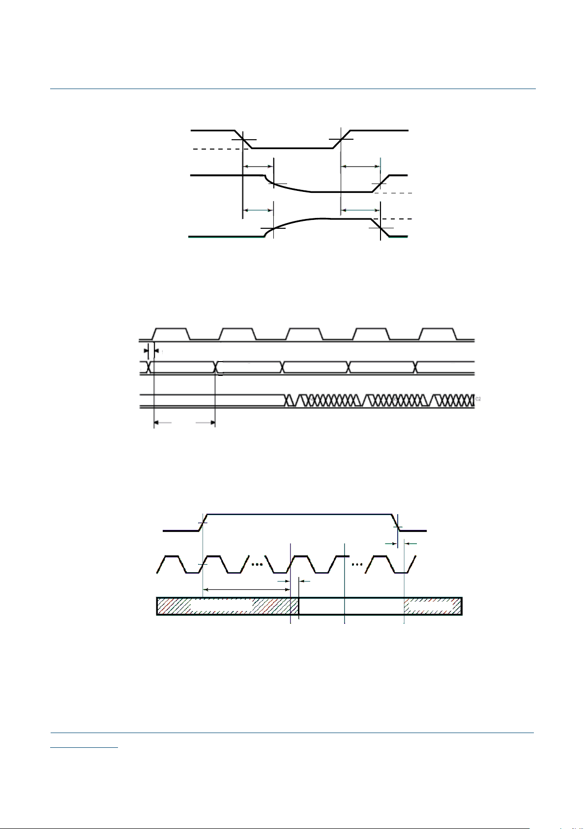
Figure 21: Channel Link Mode Serializer Transmit (Using 8:1 Mode as Example)
Figure 22: 1:1 Mode Asynchronous Level Conversion Mode Serializer Delays
[bit3][bit2][bit1][bit0][bit7][bit6][bit5][bit4]
Pad_ClkX _p/n
Pad_ ChX _p/n
TXD
[4]
[5]
[6]
[7]
[0]
ChX _txd [7:0]
ChX_txclk
Note: [N-1]
physical
positi ons wrt
Pad_ClkX_p/n while
Pad_ChX_p/n bit[n]
bit positions wrt
ChX
_txd [7:0].
tt
t
t
TXD
t
TXD
t
TXD
t
TXD
t
TXD
t
DIS
DIH
SD
denotes
refers to
bit
logical
Ch0_txd [0]
Pad_Ch0_p/n
ClkA_txclk
Pad_ClkA_p/n
t
ASD
t
ASC
www.quicklogic.com
© 2002 QuickLogic Corporation
•
•
•
•
•
•
QL82SD Device Data Sheet Rev C
Preliminary
18
SERDES Switching Characteristics - Deserializer/Receiver
a. These values include the delay resulting from application of internal compensation for data/clock skew.
Table 17: Deserializer / Receiver Switch Characteristics
CDR (10:1) Mode
Symbol Parameter Conditions Min Typ Max Units
t
RCP
ChX_rxclk Period 28.5 T 40.0 nS
t
RDC
ChX_rxclk Duty Cycle 45 50 55 %
t
DD
Deserializer Delay
Figure 23
2
× t
RCP
+ 1.5 2 × t
RCP
+ 2.5 2 × t
RCP
+ 3.5 nS
t
RXPD
ChX_rxclk to ChX_rxd[9..0] 1.5 2.5 3.5 nS
t
DSR1
Deserializer PLL Lock Time
from powered-down state
Figure 24: 25 MHz
Figure 24: 50 MHz
5
8
uS
uS
t
DSR2
Deserializer PLL Lock Time from SYNCPAT
Figure : 25 MHz
Figure : 50 MHz
1
0.75
uS
uS
t
DJIT
Pad_ChX_p/n Jitter
25 MHz
50 MHz
±350
±200
pS
pS
Channel Link (8:1, 7:1, 4:1) Mode
Symbol Parameter Conditions Min Typ Max Units
t
RCP
ChX_rxclk Period T nS
t
RDC
ChX_rxclk Duty Cycle 45 50 55 %
t
DD
Deserializer Delay
Figure 26
2
× t
RCP
+ 1.5 2 × t
RCP
+ 2.5 2 × t
RCP
+ 3.5 nS
t
RXPD
ChX_rxclk to ChX_rxd[N-1..0] 1.5 2.5 3.5 nS
t
RXDS
Pad_ChX_p/n Setup to Strobe Position 150 200 pS
t
RXDH
Pad_ChX_p/n Hold to Strobe Position 150 200 pS
t
SCD
Pad_ClkX_p/n to Serial Clock Delay
a
0.6 0.8 1 nS
t
SCP
Serial Clock Period T/mode nS
t
RXD[N-1]
Receiver Input Strobe Position for Bit [N-1] [N-1]
× t
SCP
+ 1.1 [N-1] × t
SCP
+ 2.4 nS
t
DSR1
Deserializer PLL Lock Time from
powered-down state
Figure 24: 25 MHz
Figure 24: 50 MHz
5
8
uS
uS
t
DJIT
Pad_ChX_p/n Jitter
25 MHz
50 MHz
±300
±150
pS
pS
Asynchronous Level Conversion (1:1) Mode
t
ADD
Asynchronous Deserializer Delay -
Data Channel
Figure 27
1.7 nS
t
ADC
Asynchronous Serializer Delay -
Channel Clock
a
0.6 0.8 1 nS
LVDS Link
Frequency
Compression
Mode
-1
Mode Dependent
LVDS Link
Frequency
Compression
Mode
-1
Mode Dependent

© 2002 QuickLogic Corporation
•
•
•
•
•
•
QL82SD Device Data Sheet Rev C
Preliminary
19
www.quicklogic.com
Figure 23: 10:1 Mode Deserializer Receive with Embedded Clock
Figure 24: Deserializer PLL Lock Time from Power Down
Figure 25: 10:1 Mode Deserializer PLL Lock Time from SYNCPAT
RXPD
DD
t
A
B
Ch0_txclk
Ch0_rxd[9:0]
Ch0_rxclk
pad_Ch0_p/n
t
2.0V
Enable
Chx_txclk
Pad_Chx_p/n
Chx_lock
Chx-rxd
[N-1,0]
Chx_rxclk
OE
t
ZHLK
DSR1
t
SYNC patterns
ZHR or
ZLR
t
t
Data
t
HZR ortLZR
SYNC Symbol or DIN0-9
1.5V
0.8V
Enable
Chx_txclk
Pad_Chx_p/n
Chx_lock
Chx-rxd
[N-1,0]
Chx_rxclk
OE
VCC
DSR2
t
SYNC patterns
Data
ZLR
t
t
ZHR or
SYNC Symbol or DIN0-9
t
HZR ortLZR
0.0V
0.8V
1.2V
1.0V

www.quicklogic.com
© 2002 QuickLogic Corporation
•
•
•
•
•
•
QL82SD Device Data Sheet Rev C
Preliminary
20
Figure 26: Channel Link Mode Deserializer Receive (Using 8:1 Mode as Example)
Figure 27: 1:1 Mode Asynchronous Level Conversion Mode Deserializer Delays
SERDES Bit Error Rate
The following table indicates the SERDES bit error rate at TA = 25° C and
PLLVcc = 2.5 V unless otherwise specified.
Table 18: Serializer/Deserializer Bit Error Rate
Modes Bit Error Rate
10:1 < 1 x 10
-12
8:1 < 1 x 10
-12
7:1 < 1 x 10
-12
4:1 < 1 x 10
-12
[bit3] [bit2] [bit1] [bit0] [bit7] [bit6] [bit5] [bit4]
Pad_Clkx
_p/n
Pad_Chx_p/n
SerialClock
(Internal)
RXD [ 1] max
[0] max
[1] min
[0] min
Chx_rxclk
Chx_rxd [7:0]
Note:
[N-1] denotes
physical strobe positions
wrt Pad_ClkX_p/n
while
Pad_ChX_p/n bit[n] refers
logical bit positions
wrt
ChX
_
rxd
[7:0].
t
t
t
RXD
t
RXD
t
RXD
t
t
t
t
RCP
SCP
SCD
Strobe
RXDS
RXDH
t
t
RXPD
DD
RXD
t
to
Ch0_txd [0]
Pad_Ch0_p/n
ClkA_txclk
Pad_ClkA_p/n
t
ASD
t
ASC

© 2002 QuickLogic Corporation
•
•
•
•
•
•
QL82SD Device Data Sheet Rev C
Preliminary
21
www.quicklogic.com
Electrical Specification - Programmable Fabric
DC Characteristics
DC Input/Output Levels
NOTE:
The above table gives the programmable logic timing model for the QuickSD device.
The programmable logic includes the following major elements: Super Logic (Flip-Flop and
Combinational Circuit), Clock, and I/O.
Table 19: DC Characteristics
Symbol Parameter Conditions Min Max Units
I
I
I or I/O Input Leakage Current VI = V
CCIO
or GND -10 10 µA
I
OZ
3-State Output Leakage Current VI = V
CCIO
or GND -10 10 µA
C
I
Input Capacitance
a
a. Capacitance is sample tested only. Clock pins are 12 pF maximum.
8pF
I
OS
Output Short Circuit Current
b
b. Only one output at a time. Duration should not exceed 30 seconds.
Vo = GND -15 -180 mA
V
o
= V
CC
40 210 mA
I
CC
D.C. Supply Current
c
c. For -4/-5/-6/-7 commercial grade devices only. Maximum ICC is 3 mA for all industrial grade devices.
VI,Vo =V
CCIO
or GND 0.50 (typ) 2 mA
I
CCIO
D.C. Supply Current on V
CCIO
02mA
I
REF
D.C. Supply Current on V
REF
-10 10 µA
I
PD
Pad Pull-down (programmable) V
CCIO
= 3.6 V 150 µA
Table 20: DC Input/Output Levels
V
REF
V
IL
V
IH
V
OL
V
OH
I
OLIOH
V
MINVMAXVMIN
V
MAX
V
MIN
V
MAX
V
MAX
V
MIN
mA mA
LVTTL n/a n/a
-0.3 0.8 2.0 V
CCIO
- 0.3 0.40 2.40 2.0 -2.0
LVCMOS2 n/a n/a -0.3 0.7 1.7 V
CCIO
- 0.3 0.70 1.70 2.0 -2.0
GTL+ 0.88 1.12 -0.3 V
REF
- 2.0 V
REF
+ 2.0 V
CCIO
- 0.3 0.60 n/a 40 n/a
PCI n/a n/a -0.3 0.30 × V
CC
0.50 × VCCV
CCIO
- 0.5 0.10 × V
CC
0.90 × V
CC
1.5 -0.5
SSTL2 1.15 1.35
-0.3 V
REF
- 0.18 V
REF
+ 0.18 V
CCIO
+ 0.3 0.74 1.76 7.6 -7.6
SSTL3 1.30 1.70 -0.3 V
REF
- 0.20 V
REF
+ 2.0 V
CCIO
+ 0.3 1.10 1.90 8.0 -8.0

www.quicklogic.com
© 2002 QuickLogic Corporation
•
•
•
•
•
•
QL82SD Device Data Sheet Rev C
Preliminary
22
Super Logic (Flip-Flop and Combinational Circuit) AC Characteristics at
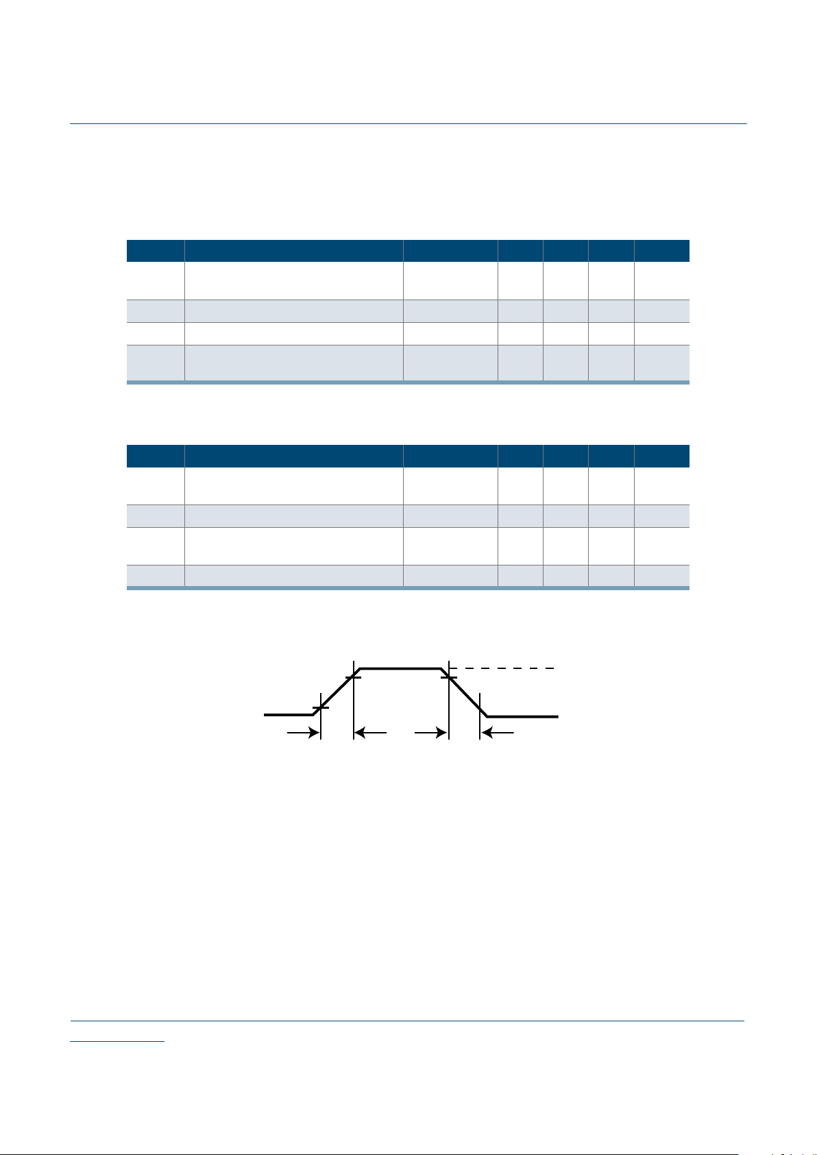
VCC = 2.5 V, TA = 25o C (K = 1)
Figure 28: Super Logic Cell Flip-Flop Structure
Figure 29: Combinational Delay for Logic Cell
Table 21: Logic Cells
Symbol Parameter Condition
Propagation delay (ns)
Fanout = 1
t
PD
Combinational Delay
a
a. Stated timing for worst case Propagation Delay over process variation at VCC = 2.5 V and
TA = 25 °C. Multiply by the appropriate Delay Factor, K, for speed grade, voltage and temperature
settings as specified in the operating range.
Figure 29 0.257
t
SU
Setup Time
b
b. These limits are derived from a representative selection of the slowest paths through the logic cell
including typical net delays. Worst case delay values for specific paths should be determined from
timing analysis of your particular design.
Figure 30
0.22
t
H
Hold Time 0
t
CLK
Clock to Q Delay Figure 31 0.255
t
CWHI
Clock High Time
Figure 32
0.46
t
CWLO
Clock Low Time 0.46
t
SET
Set Delay
Figure 33
0.18
t
RESET
Reset Delay 0.09
t
SW
Set Width 0.30
t
RW
Reset Width 0.30
reset
clk
d
set
q
tPD
input
output

© 2002 QuickLogic Corporation
•
•
•
•
•
•
QL82SD Device Data Sheet Rev C
Preliminary
23
www.quicklogic.com
Figure 30: Setup and Hold Time for Flip-Flop
Figure 31: Delay from Clock Input to Flip-Flop Q Output
Figure 32: Clock High and Low Time for Flip-Flop
Figure 33: Timing Requirements for Flip-Flop SET and RESET
tSU
tH
Input (d)
clk

www.quicklogic.com
© 2002 QuickLogic Corporation
•
•
•
•
•
•
QL82SD Device Data Sheet Rev C
Preliminary
24
Clock AC Characteristics at VCC = 2.5 V, TA = 25 oC (K = 1)
Figure 34: Clock Structure
I/O AC Characteristics at VCC = 2.5 V, TA = 25 oC (K = 1)
Figure 35: I/O Structure
Table 22: Clock Performance
Clock Performance
Global Dedicated
Logic Cells 1.51 ns 1.59 ns
I/Os 2.06 ns 1.73 ns
Skew 0.55 ns 0.14 ns
Table 23: Input Register Cell
Symbol
Input Register Cell Only
Parameter Propagation Delay (ns)
t
PGCK
Global clock pin delay to quad net 1.34
t
BGCK
Global clock buffer delay (quad net to flip
flop)
0.56
programmable clock
Hardware Clock
Global Clock Buffer
Global Clock
PGCK
BGCK
t
t

© 2002 QuickLogic Corporation
•
•
•
•
•
•
QL82SD Device Data Sheet Rev C
Preliminary
25
www.quicklogic.com
Figure 36: Input Register Cell
Table 24: Input Register Cell
Symbol
Input Register Cell Only
Parameter
Propagation
Delay (ns)
t
ISU
Input Register Setup Time: the amount of time the synchronous
input of the flip flop must be stable before the active clock edge.
3.12
t
IH
Input Register Hold Time: the amount of time the synchronous input
of the flip flop must be stable after the active clock edge.
0
t
ICLK
Input Register Clock to Q: the amount of time taken by the flip flop
to output after the active clock edge.
1.08
t
IRST
Input Register Reset Delay: the amount of time between when the
flip flop is “reset” (low) and when Q is consequently “reset” (low).
0.99
t
IESU
Input Register Clock Enable Setup Time: the amount of time
“enable” must be stable before the active clock edge.
0.37
t
IEH
Input Register Clock Enable Hold Time: the amount of time “enable”
must be stable after the active clock edge.
0
PAD
E
R
Q
D
+
-
TIN, TINI
TISU
TICLK
tSID

www.quicklogic.com
© 2002 QuickLogic Corporation
•
•
•
•
•
•
QL82SD Device Data Sheet Rev C
Preliminary
26
Table 25: Standard Input Delays
Figure 37: Input Register Timing
Figure 38: Output Register Cell
Symbol Parameter
Propagation
delay (ns)
Standard
Input Delays
To get the total input delay and this delay to tISU
t
SID (LVTTL)
LVTTL input delay: Low Voltage TTL for 3.3 V applications 0.34
t
SID (LVCMOS2)
LVCMOS2 input delay: Low Voltage CMOS for 2.5 V and
lower applications
0.42
t
SID (GTL+)
GTL+ input delay: Gunning Transceiver Logic 0.68
t
SID (SSTL3)
SSTL3 input delay: Stub Series Terminated Logic for 3.3 V 0.55
t
SID (SSTL2)
SSTL2 input delay: Stub Series Terminated Logic for 2.5V 0.607
R
CLK
D
Q
tISU
tIH
tICLK
tIESU
tIEH
tIRST
E
PAD
OUTPUT
REGISTER

© 2002 QuickLogic Corporation
•
•
•
•
•
•
QL82SD Device Data Sheet Rev C
Preliminary
27
www.quicklogic.com
Table 26: Output Register Cell
Figure 39: Output Register Cell Timing
Electrical Specification - RAM Block
Figure 40: RAM Module
Symbol Parameter Propagation delay (ns)
Output Register Cell Only
t
OUTLH
Output Delay low to high (10% of H) 0.40
t
OUTHL
Output Delay high to low (90% of H) 0.55
t
PZH
Output Delay tri-state to high (10% of Z) 2.94
t
PZL
Output Delay tri-state to low (90% of Z) 2.34
t
PHZ
Output Delay high to tri-State 3.07
t
PLZ
Output Delay low to tri-State 2.53
t
CO
Clock to out delay 3.15 (fast slew) 10.2(slow slew)
L
H
L
H
tOUTLH
tOUTHL
L
H
Z
tPZH
L
H
Z
tPZL
L
H
Z
tPLZ
L
H
Z
tPHZ
WA
WD
WE
WCLK
RE
RCLK
RA
RD
[9:0]
[17:0]
[9:0]
[17:0]
MODE ASY NCRD
[1:0]

www.quicklogic.com
© 2002 QuickLogic Corporation
•
•
•
•
•
•
QL82SD Device Data Sheet Rev C
Preliminary
28
RAM Cell Synchronous Write Timing
Table 27: RAM Cell Synchronous Write Timing
Figure 41: RAM Cell Synchronous Write Timing
Symbol Parameter
Propagation
delay (ns)
t
SWA
WA setup time to WCLK: the amount of time the WRITE ADDRESS
must be stable before the active edge of the WRITE CLOCK
0.675
t
HWA
WA hold time to WCLK: the amount of time the WRITE ADDRESS
must be stable after the active edge of the WRITE CLOCK
0
t
SWD
WD setup time to WCLK: the amount of time the WRITE DATA must
be stable before the active edge of the WRITE CLOCK
0.654
t
HWD
WD hold time to WCLK: the amount of time the WRITE DATA must
be stable after the active edge of the WRITE CLOCK
0
t
SWE
WE setup time to WCLK: the amount of time the WRITE ENABLE
must be stable before the active edge of the WRITE CLOCK
0.623
t
HWE
WE hold time to WCLK: the amount of time the WRITE ENABLE must
be stable after the active edge of the WRITE CLOCK
0
t
WCRD
WCLK to RD (WA=RA): the amount of time between the active WRITE
CLOCK edge and the time when the data is available at RD
4.38
tSWA
tSWD
tSWE
tHWA
tHWD
tHWE
tWCRD
old data
new data
WCLK
WA
WD
WE
RD
© 2002 QuickLogic Corporation
•
•
•
•
•
•
QL82SD Device Data Sheet Rev C
Preliminary
29
www.quicklogic.com
RAM Cell Read Timing
Table 28: RAM Cell Synchronous and Asynchronous Read Timing
Figure 42: RAM Cell Synchronous and Asynchronous Read Timing
Symbol Parameter
Propagation
delay (ns)
RAM Cell Synchronous Read Timing
t
SRA
RA setup time to RCLK: the amount of time the READ ADDRESS
must be stable before the active edge of the READ CLOCK
0.686
t
HRA
RA hold time to RCLK: the amount of time the READ ADDRESS
must be stable after the active edge of the READ CLOCK
0
t
SRE
RE setup time to WCLK: the amount of time the READ ENABLE
must be stable before the active edge of the READ CLOCK
0.243
t
HRE
RE hold time to WCLK: the amount of time the READ ENABLE
must be stable after the active edge of the READ CLOCK
0
t
RCRD
RCLK to RD: the amount of time between the active READ CLOCK
edge and the time when the data is available at RD
4.38
RAM Cell Asynchronous Read Timing
r
PDRD
RA to RD: amount of time between when the READ ADDRESS is
input and when the DATA is output
2.06
RE
RD
RCLK
RA
TSRA THRA
TSRE
THRE
OLD data NEW data
TRCRD
RPDRD

www.quicklogic.com
© 2002 QuickLogic Corporation
•
•
•
•
•
•
QL82SD Device Data Sheet Rev C
Preliminary
30
LVDS SERDES Description
LVDS SERDES Applications
The QL82SD device in the QuickLogic QuickSD ESP (Embedded Standard Product) device
family provides a completely integrated configurable Serializer/Deserializer interface solution
combined with 536 K system gates of customizable logic. This device provides a means to
receive and transmit high-speed serial data and implement any proprietary high-speed serial
link.
The QL82SD device is a high performance serializer/deserializer chip. It can be combined
with FIFO buffer memory to build a complete serial link. The need for external FIFOs can be
eliminated by configuring the available internal RAM as two 256 x 36 FIFOs.
The embedded SERDES core is a full duplex design with a serialization section for
transmission and a deserialization section for reception. The transmitter and receiver can be
configured for level conversion (1:1), signals that transmit a clock signal with the data
(1:4, 1:7, 1:8), or applications that require clock recovery (1:10).
The embedded SERDES core has a system interface that emulates a synchronous FIFO for
ease of use. FIFOs allow maximum sustained performance of 600 MB/s running a full duplex
link. Their function is to handle the asynchronous interface between the bus data rate and
the different serial data rates, and handle phase and frequency differences inherent in serial
links. Internal FIFOs of 256
×××× 36 or 512 ×××× 16 can be cascaded with external FIFOs to
expand the buffering to the desired size.
The QL82SD is a versatile part that allows the system designer to create proprietary or
standardized serial links by taking advantage of some, or all, of the embedded features. It has
a number of useful features for system designers of proprietary links with additions of
embedded computational units and customizable I/O.
LVDS SERDES Block Functional Description
The QuickSD SERDES consists of a physical layer for high-speed serial communications,
handling all data translations, clocking and timing. The core is made up of eight data
channels and two channel clocks. These blocks contain the circuitry necessary for all the data
muxing and de-muxing, clock multiplication and division, clock and data phase alignment,
and clock recovery and encoding. The core can be configured to support systems that
transmit a separate clock signal or that have the clock embedded into the data stream and
require clock recovery.

© 2002 QuickLogic Corporation
•
•
•
•
•
•
QL82SD Device Data Sheet Rev C
Preliminary
31
www.quicklogic.com
LVDS SERDES Data Channel Configuration
A representation of the SERDES data channel is shown in Figure 43. The device consists of
eight identical data channels.
Figure 43: SERDES Channel 0
Each SERDES data channel can be operated independently. The data channels are
transceivers, so they can either send or receive data on the serial LVDS wire pair. The
direction of transfer is selected with the ChX_oe pin. If this pin is high, the channel is in
transmit mode, if this pin is low, the channel is in receive mode.
The data channel can be configured to deal with different parallel data widths and clocking
mechanisms,
Table 2 9 shows the settings for the ChX_mode[3:0] pins and the modes that
they refer to.
For the Channel Clock A/B modes, see
“LVDS SERDES Channel Clock Configuration” on
page 32
for more details. If the data channel is not needed, then it can be powered down (to
reduce overall device power) by tying the ChX_en signal low. This signal must be held high
for normal operation.
For a detailed description of how to use the various modes of the data channel to transmit
and receive data, see
“LVDS SERDES Transmit and Receive Operation” on page 33.
Table 29: ChX_mode[3:0]
ChX_mode[3] Description
bit [3]
Low Frequency (1), High Frequency (0)
Determines high or low frequency lock range for internal SERDES PLL.
When this bit is set to ‘1’, the low frequency range is selected.
When this bit is set to ‘0’, the high frequency range is selected.
bit [2]
In 10:1 mode, this bit must be set to ‘0’.
In channel clock mode, the pin setting does not matter.
bit [1] Embedded clock mode (0), channel-clock (1)
bit [0] CLKA (1), CLKB (0) channel clock select
Ch0_rst
Ch0_lock
Ch0_en
Ch0_oe
Ch0_pre_emp
Ch0_mode[3:0]
Ch0_sync
Ch0_txclk
Ch0_rxclk
Ch0_txd[9:0]
Ch0_rxd[9:0]
pad_Ch0-p
pad_Ch0_n
SERDES
Channel 0

www.quicklogic.com
© 2002 QuickLogic Corporation
•
•
•
•
•
•
QL82SD Device Data Sheet Rev C
Preliminary
32
LVDS SERDES Channel Clock Configuration
There are two SERDES channel clocks within the core. Figure 44 shows a representation of
the channel clock. Each channel clock is identical.
Figure 44: SERDES CLK A
Each of the two SERDES channel clocks can be configured independently. They can be
configured to act as the transmit or receive clock for up to 8 SERDES data channels (for serial
links where the clock is provided as a separate LVDS wire pair). Alternatively, the channel
clock can be configured as a simple bi-directional IO pin, where the internal signals are
CMOS, but the external pin is LVDS. In such a case, the I/O will act simply as a level
converter.
Since the channel clock may act as a transmit or receive clock (or as an input or output signal
in data mode), the direction of the channel clock must be selected with the ClkX_oe pin. If
this pin is high, then the channel clock is transmitting a clock (or acting as an output signal
in data mode). If this pin is low, then the channel clock is receiving a clock (or acting as an
input signal in data mode).
When the channel clocks are used to act as the transmit or receive clock for one or more
data channels, then four modes are available, using the CLKx_MODE[1:0] input.
Table 30
shows these modes.
When a channel clock is configured with ClkX_MODE[1:0] equal to 01, 10, or 11, then any
of the data channels can be configured to use that channel clock as its clock, by setting the
data channel's ChX_MODE inputs to point to the correct channel clock. See the
Section ,
“LVDS SERDES Data Channel Configuration,” on page 31
for more information.
When the channel clock is configured with ClkX_MODE[1:0] equal to 00, the channel clock
becomes a simple LVDS-to-CMOS level converter.
When ClkX_oe is high, the channel clock will be configured as an output, in which the data
supplied on the ClkX_txclk pin is converted to LVDS and comes out on the pad_ClkX_p and
pad_ClkX_n external LDVS signals asynchronously.
When ClkX_oe is low, the channel clock is configured as an LVDS input, in which the LVDS
signal on pad_ClkX_p and pad_ClkX_n is converted to CMOS levels and enters the device
on the ClkX_rxclk pin.
Table 30: ClkX_mode[1:0]
ClkX_mode[1:0] Mode
00 1:1 mode (no PLL)
01 4:1 mode
10 7:1 mode
11 8:1 mode
ClkA_oe
ClkA_rxclk
ClkA_pre_emp
ClkA_en
ClkA_mode[1:0]
ClkA_txclk
pad_ClkA_p
pad_ClkA_n
SERDES
CLKA

© 2002 QuickLogic Corporation
•
•
•
•
•
•
QL82SD Device Data Sheet Rev C
Preliminary
33
www.quicklogic.com
Any data channel ca n also b e config ured as a level t r anslat or. Thi s is done by setting that data
channel's ChX_mode[3:0] input to point to a channel clock (A or B) which has also been
configured in level translator mode.
LVDS SERDES Transmit and Receive Operation
The SERDES core can transmit and receive serial data across LVDS wires in many different
formats. This section describes each of the various transmit and receive formats.
Transmit 10-bit Data With Embedded Clock
The waveform in Figure 19, illustrates how 10-bit data can be transmitted serially on the
differential LVDS outputs.
NOTE:
The pad_ChX_p and pad_ChX_n outputs in the diagram are representing the data
changes which occur on a pair of LVDS signals.
When the SERDES is in 10-bit mode, no separate clock signal is needed, since the clock is
embedded within the serial data stream. In
Figure 19, you will notice that at t
DIS
the rising
edge of ChX_txclk registers the 10-bit data value B within the SERDES core. After about one
clock period of ChX_txclk, the serialized data begins to appear on the LVDS outputs
(pad_ChX_p and pad_ChX_n) in the following sequence:
1. First, a logic 1 is transmitted, which is the start bit, and part of the data used to transmit
the clock.
2. Then each of the 10 bits of the data value B is transmitted in sequence.
3. Finally, a logic 0 is transmitted, which is the stop bit (MSB first). This stop bit is the
remaining part of the embedded clock.
NOTE:
By using a stop bit value of 0 and a start bit value of 1, there is always a guaranteed
0 to 1 transition in the bitstream (the end of one frame and the beginning of the next).
Because of this, the receiver is able to recover the embedded clock from the serial bit stream.
The pertinent timing parameters shown in
Figure 19 are:
• t
DIS
is the setup time needed for the ChX_txd bus relative to the ChX_txclk clock
• t
DIH
is the hold time for the ChX_txd relative to the ChX_txclk clock
Receive 10-bit Data With Embedded Clock
In 10-bit mode, the clock is embedded in the serial data stream on the pad_ChX_p and
pad_ChX_n LVDS signal (shown in
Figure 23) as one signal, but actually is a pair of
differential signals). When using the SERDES data channel in 10-bit receive mode, a
reference clock is needed which matches the parallel clock rate of the transmitter (shown in
Figure 23 as ChX_txclk). There is no timing phase relationship between the reference clock
and the received parallel clock (ChX_rxclk), but the two clocks will have the same frequency.
NOTE:
The serial data bits are transmitted with a 0 as a stop bit and a 1 as a start bit, and.
The SERDES block recovers the clock from this data stream, as shown with the ChX_rxclk
waveform (
Figure 23). The parallel 10-bit data is also recovered and timed appropriately with
the recovered clock.
The pertinent timing parameters shown in
Figure 23 are:

www.quicklogic.com
© 2002 QuickLogic Corporation
•
•
•
•
•
•
QL82SD Device Data Sheet Rev C
Preliminary
34
•
t
DD
is the delay from the rising edge of the start bit in the serial bitstream to the rising
edge of the recovered parallel clock
• t
RXPD
is the propagation delay time provided for the recovered data with respect to the
recovered clock.
Transmit 8-bit Data With Channel Clock
When the SERDES is in 8-bit mode, it must be configured to use a channel clock. The
waveforms shown in
Figure 21 show the parallel transmit clock provided by the user to the
clock channel (ClkX_txclk), and the converted channel clock on the LVDS outputs of the
channel clock (pad_ClkX_p and pad_ClkX_n).
NOTE:
The output of the channel clock has the same period as the parallel transmit clock.
This is done to frame the serial data transmitted on the pad_ChX_p and pad_ChX_n pins.
The LVDS channel clock (pad_ClkX_p and pad_ClkX_n) is multiplied up by the receiver to
capture each bit of the transmitted data.
The 8-bit data is converted to a simple serial bit stream.
The pertinent timing parameters shown in
Figure 21 are:
• t
DIS
is the setup time needed on the parallel transmit data (ChX_txd[7:0] with respect to
the parallel transmit clock (ClkX_txclk)
• t
DIH
is the hold time needed on the parallel transmit data (ChX_txd[7:0] with respect to
the parallel transmit clock (ClkX_txclk)
• t
SD
is the clock delay between the rising edge of the parallel transmit clock to the rising
edge of the LVDS channel clock
• t
TXD[N-1]
is the serial data physical bit position with respect to the LVDS channel clock.
NOTE:
t
TXD[N-1]
denotes physical bit positions wrt pad_ClkX_p/n while pad_ChX_p/n bit[n]
refers to logical bit positions wrt ChX_txd[7:0].
Receive 8-bit Data With Channel Clock
The SERDES in 8-bit receive mode receives serial data on the pad_ChX_p and pad_ChX_n
LVDS input, and a clock on the pad_ClkX_p and pad_ClkX_n LVDS input (see
Figure 26 ).
The LVDS input clock is multiplied by 8 within the SERDES core to capture the 8 bits of data
from the pad_ChX_p and pad_ChX_n serial bitstream. The parallelized data goes out on the
ChX_rxd internal 8-bit bus, and the re-timed parallel clock goes out on the ClkX_rxclk pin.
The pertinent timing parameters shown in this diagram are:
• t
DD
is the delay between the first bit of the serial data showing up in the serial bit stream
and the rising edge of the retimed parallel clock corresponding to the same data frame
• t
RXPD
is the propagation delay time provided for the recovered data with respect to the
recovered clock
• t
RXDS
is the setup time needed for the serial data on the pad_ChX_p and pad_ChX_n
LVDS inputs to the rising edge of the internal serial clock strobe
• t
RXDH
is the hold time needed for the serial data on the pad_ChX_p and pad_ChX_n
LVDS inputs relative to the internal serial clock strobe

© 2002 QuickLogic Corporation
•
•
•
•
•
•
QL82SD Device Data Sheet Rev C
Preliminary
35
www.quicklogic.com
• t
SCD
is the delay between the rising edge of the LVDS channel clock and the first rising
edge of the multiplied internal serial clock corresponding to the same data frame.
• t
RXD[N-1]
is the internal clock strobe positions with respect to the rising edge of the LVDS
channel clock
NOTE:
t
RXD[N-1]
denotes physical strobe positions with respect to pad ClkX_p/n while
pad_ChX_p/n bit[n] refers to logical bit positions with respect to ChX_rxd[7:0]
Asynchronous Level Conversion Mode for the Data Channel and
Channel Clock
When the SERDES data channel ChX_mode[3:0] pins are set to use a channel clock which
is in level translator mode, then that data channel is also in level translator mode. In level
translator mode, the data channel only converts the internal CMOS signal to LVDS (for
output mode), or vice versa for input mode.
When the data channel or channel clock is in this asynchronous signal translation mode, and
configured as outputs (ChX_oe or ClkX_oe high) the output mode waveforms in
Figure 22
apply.
When the data channel or channel clock is in this asynchronous signal translation mode, and
configured as inputs (ChX_oe or ClkX_oe low) the input mode waveforms in
Figure 27 apply.
Programmable Fabric Description
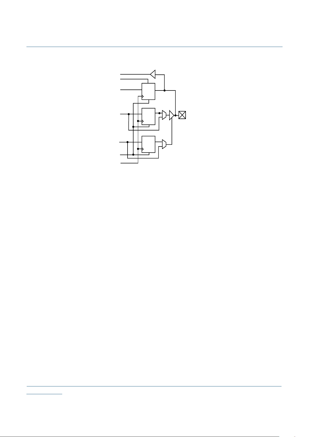
The QuickSD device features an enhanced Super Logic Cell with an additional D flip-flop
register and associated control logic. This advanced architectural approach addresses today's
highly register intensive designs.
The QuickSD logic Supercell structure, shown in
Figure 45, is similar to the .35 mm
QuickLogic logic cell with the addition of a second register. Both registers share CLK, SET
and RESET inputs. The second register has a two-to-one multiplexer controlling its input.
This register can be loaded from the NZ output or directly from a dedicated input.
NOTE:
The input "PP" is not an "input" in the classical sense. It can only be tied high or low
using default links only and is used to select which path "NZ" or "PS" is used as an input to
the register. All other inputs can be connected not only to "tiehi" and "tielo" but to multiple
routing channels as well.
The complete logic cell consists of two 6-input AND gates, four two-input AND gates, seven
two-to-one multiplexers, and two D flip-flops with asynchronous SET and RESET controls.
The cell has a fan-in of 30 (including register control lines) and fits a wide range of functions
with up to 17 simultaneous inputs. It has six outputs, of which four are combinatorial and
two are registered. The high logic capacity and fan-in of the logic cell accommodate many
user functions with a single level of logic delay while other architectures require two or more
levels of delay.

www.quicklogic.com
© 2002 QuickLogic Corporation
•
•
•
•
•
•
QL82SD Device Data Sheet Rev C
Preliminary
36
Figure 45: SERDES Logic Cell
RAM Block Description
General Description
The QuickSD device includes multiple dual-port 2,304-bit RAM modules for implementing
RAM and FIFO functions. Each module is user-configurable into four different block
organizations. Modules can also be cascaded horizontally to increase their effective width or
vertically to increase their effective depth as shown in the following figure. The RAM can also
be configured as a modified Harvard Architecture, similar to those found in DSPs.
Figure 46: SERDES 2,304-bit RAM Module
QS
A1
A2
A3
A4
A5
A6
OS
OP
B1
B2
C1
C2
MP
MS
D1
D2
E1
E2
NP
NS
F1
F2
F3
F4
F5
F6
PS
PP
QC
QR
AZ
OZ
QZ
NZ
Q2Z
FZ
MODE [1:0]
WA [9:0]
WD [17:0]
WE
WCLK
RCLK
ASYNCRD
RA [9:0]
RD [17:0]
RE
2,304-bit Module

© 2002 QuickLogic Corporation
•
•
•
•
•
•
QL82SD Device Data Sheet Rev C
Preliminary
37
www.quicklogic.com
There are 36 RAM blocks within the QuickSD device, for a total of 82.9 Kbits of RAM. Using
two "mode" pins, designers can configure each module into 128 x 18 (Mode 0), 256 x 9
(Mode 1), 512 x 4 (Mode 2), or 1024 x 2 blocks (Mode 3). The blocks are also easily
cascadable to increase their effective width and/or depth. See
Figure 47 for cascaded RAM
modules.
Figure 47: Cascaded RAM Modules
The RAM modules are dual-port, with completely independent READ and WRITE ports and
separate READ and WRITE clocks. The READ ports support asynchronous and synchronous
operation, while the WRITE ports support synchronous operation. Each port has 18 data
lines and 10 address lines, allowing word lengths of up to 18 bits and address spaces of up
to 1,024 words. Depending on the mode selected, however, some higher order data or
address lines may not be used.
The Write Enable (WE) line acts as a clock enable for synchronous write operation.
The Read Enable (RE) acts as a clock enable for synchronous READ operation (ASYNCRD
input low), or as a flow-through enable for asynchronous READ operation (ASYNCRD input
high).
Designers can cascade multiple RAM modules to increase the depth or width allowed in
single modules by connecting corresponding address lines together and dividing the words
between modules.
A similar technique can be used to create depths greater than 512 words. In this case address
signals higher than the ninth bit are encoded onto the write enable (WE) input for WRITE
operations. The READ data outputs are multiplexed together using encoded higher READ
address bits for the multiplexer SELECT signals.
The RAM blocks can be loaded with data generated internally (typically for RAM or FIFO
functions). The RAM achieve 155 MHz performance for the lowest speed grade devices
when using multiple blocks cascaded together.
Multiple Accessing of Memories
The extremely fast RAM can be used in designs that require multiple memory accessing. The
RAM achieves 280 MHz performance for the fastest speed grade and 155 MHz
performance for the lowest speed grade devices when using multiple blocks cascaded
together. Write through of DATA is also possible with the QuickLogic RAM.
WDATA
WADDR
WDATA
RDATA
RADDR
RDATA
RAM
Module
(2304 bits)
RAM
Module
(2304 bits)

www.quicklogic.com
© 2002 QuickLogic Corporation
•
•
•
•
•
•
QL82SD Device Data Sheet Rev C
Preliminary
38
ECU Block Description
ECU Block General Description
Traditional Programmable Logic architectures do not implement arithmetic functions
efficiently or effectively. These functions require high logic cell usage while garnering only
moderate performance results. By embedding a dynamically reconfigurable computational
unit, the QuickSD device can address various arithmetic functions efficiently and effectively
providing for a robust DSP platform—this approach offers greater performance than
traditional programmable logic implementations. The ECU block is ideal for complex DSP,
filtering, and algorithmic functions. The QuickSD device architecture will allow functionality
above and beyond that achievable using DSP processors or programmable logic devices. The
embedded block is implemented at the transistor level with the following block diagram.
Figure 48: SERDES ECU Block Diagram
ECU Mode Select
The ECU block can be configured for eight arithmetic functions via an instruction as shown
in
Tabl e 31 . The modes for the ECU block are Dynamically Re-programmable through the
Instruction Set Sequencer.
Table 31: Instruction Set Sequencer
Instruction Set Operation
0 0 0 Multiply
0 0 1 Multiply - Add
0 1 0 Accumulate
0 1 1 Add
1 0 0 Multiply (registered)
a
a. A[15:0] set to zero.
1 0 1 Multiply - Add (registered)
1 1 0 Multiply Accumulate
1 1 1 Add (registered)
Abus
16
Xbus
8
Ybus
8
Ibus
3
Sign
1
Rbus
17
88
16 16
Multiply Add Register
Sequencer Memory Logic Cell

© 2002 QuickLogic Corporation
•
•
•
•
•
•
QL82SD Device Data Sheet Rev C
Preliminary
39
www.quicklogic.com
Clock Networks Description
Global Clocks
In the QuickSD device, there are nine global clock networks: one is dedicated and eight are
programmable . Global clocks can drive logic cell, I/O, ECU blocks and RAM registers in the
device. Five global clocks will have access to a Quad Net (local clock network) connection
with a programmable connection to the register inputs.
Figure 49 gives the global clock
methodology
Figure 49: Global Clock
Quad-Net Network
There are five Quad-Net local clock networks in each quadrant for a total of 20 in a device.
Each Quad-Net is local to a quadrant. Quad-Net is multiplexed with the clock buffer before
driving the column clock buffers.
www.quicklogic.com
© 2002 QuickLogic Corporation
•
•
•
•
•
•
QL82SD Device Data Sheet Rev C
Preliminary
40
Dedicated Clock
There is one dedicated clock in QuickSD devices. It connects to the clock input of the
SuperCell, I/O, and RAM registers through a hardwired connection and is multiplexed with
the programmable clock input. There are four inversions from pad to register inputs and the
dedicated clock takes on the same configuration as the global clock. The dedicated clock
provides a fast global network with low skew. You can select either the dedicated clock or the
programmable clock;
Figure 50 gives the dedicated clock circuitry within the logic cell.
Figure 50: Dedicated Clock Circuitry
The performance of the dedicated clock is given in Table 3 2
Table 32: Dedicated Clock Performance
Clock Performance
TT, 25C, 2.5 V Global Dedicated
Macro (rear) 1.51 1.59
I/O (far) 2.06 1.73
Skew 0.55 0.14
Programmable clock
Hard-wired clock
CLK

© 2002 QuickLogic Corporation
•
•
•
•
•
•
QL82SD Device Data Sheet Rev C
Preliminary
41
www.quicklogic.com
I/O Cell Structure
I/O Cell Structure General Description
The QuickSD device features a variety of distinct I/O pins to maximize performance,
functionality, and flexibility with bi-directional I/O pins and input-only pins. All input and I/O
pins are 2.5 V and 3.3 V tolerant and comply with the specific I/O standard selected. The
outputs swing from Vss to VCCIO (0 V to 3.3 V ± 10%). The VCCIO pins must be tied to
a 3.3 V supply to provide 3.3 V compliance.
If 3.3 V compliance is not required, then these pins must be tied to the 2.5 V supply.
Table 33 summarizes the I/O specifications that are supported.
As designs become more complex and requirements more stringent, varying I/O standards
are developing for specific applications. I/O standards for processors, memories and various
bus applications have become common place and a requirement for many systems. In
addition, I/O timing has become a greater issue with specific requirements for setup, hold,
clock to out, and switching times.
The QuickSD device has addressed these changing system requirements. The QuickSD
device includes a completely new I/O cell which consists of programmable I/Os as well as a
new cell structure consisting of three registers: input, output and output enable. The QuickSD
device offers banks of programmable I/O that addresses many of the new bus standards that
are popular today. In addition, the input register addresses the setup time, the output register
addresses clock-to-out time, and the OE register addresses the switching time from high
impedance to a given value.
Figure 51 shows the QuickSD device I/O cell.
Table 33: Supported I/O Specifications
/O Standard Reference Voltage Output Voltage Application
LVTTL n/a 3.3 general purpose
LVCMOS2 n/a 2.5 general purpose
PCI n/a 3.3 PCI bus applications
GTL+ 1 n/a high speed bus - Pentium Pro
SSTL3 1.5 3.3 memory bus - Hitachi, IBM
SSTL2 1.25 2.5 memory bus - Hitachi, IBM
www.quicklogic.com
© 2002 QuickLogic Corporation
•
•
•
•
•
•
QL82SD Device Data Sheet Rev C
Preliminary
42
Figure 51: QuickSD I/O Cell
The bi-directional I/O pin options can be programmed for input, output, or bi-directional
operation. Each bi-directional I/O pin is associated with an I/O cell which features an
input/feedback register, an input buffer, output/feedback register, three-state output buffer,
an output enable register, and two 2-to-1 multiplexers.
For input functions, I/O pins can provide combinatorial
registered data or both options
simultaneously to the logic array. For combinatorial input operation, data is routed from I/O
pins through the input buffer to the array logic. For registered input operation, I/O pins drive
the D input of input cell registers, allowing data to be captured with fast set-up times without
consuming internal logic cell resources.
For output functions, I/O pins can receive combinatorial or registered data from the logic
array. For combinatorial output operation, data is routed from the logic array through a
multiplexer to the I/O pin. For registered output operation, the array logic drives the D input
of the output cell register which in turn drives the I/O pin through a multiplexer. The
multiplexer allows either a combinatorial or a registered signal to be driven to the I/O pin.
The three-state output buffer controls the flow of data from the array logic to the I/O pin and
allows the I/O pin to act as an input and/or output. The buffer's output enable can be
individually controlled by a logic cell array or any pin (through the regular routing resources),
or bank-controlled through one of the global networks.
The signal can also be either combinatorial or registered. This is identical to that of the flow
for the output cell. For combinatorial control operation, data is routed from the logic array
through a multiplexer to the three-state control. For registered control operation, the array
logic drives the D input of the OE cell register which in turn drives the three-state control
through a multiplexer. The multiplexer allows either a combinatorial or a registered signal to
be driven to the three-state control.
For output functions, I/O pins can be individually configured for active HIGH, active LOW,
or open-drain inverting operation. In the active HIGH and active LOW modes, the pins of
all devices are fully 3.3 V compliant.
E
Q
R
D
E
D
R
Q
PA D
E
D
R
Q
+
-

© 2002 QuickLogic Corporation
•
•
•
•
•
•
QL82SD Device Data Sheet Rev C
Preliminary
43
www.quicklogic.com
When I/O pins are unused, the OE controls can be permanently disabled, allowing the output
cell register to be used for registered feedback into the logic array.
I/O cell registers are controlled by clock, clock enable, and reset signals, which can come
from the regular routing resources, from one of the global networks, or from two input pins
per bank of I/O's. The CLK and RESET signals share a common line, while the clock enables
for each register can be independently controlled. Additionally, the output and enable
registers will increase a device's register count. The addition of an output register will also
decrease the TCO. Since the output register does not need to drive the routing, the length
of the output path is also reduced.
Extra registers add more inputs and outputs to the I/O structure. Extra routing resources are
added to connect the I/O structure to the other parts of the device.
I/O interface support is programmable on a per bank basis. There are 4 I/O banks per chip.
Users can not mix a 2.5 volt I/O with 3.3 volt I/O on the same I/O bank.
Figure 52 illustrates
the multiple I/O bank configurations.
Figure 52: Multiple I/O Bank Configurations
Each I/O bank is independent of other I/O banks and each I/O bank has its own V
CCIO
and
V
REF
supplies. A mixture of different I/O standards can be used on the device; however, there
is a limitation as to which I/O standards can be supported within a given bank. Differential
I/O can be shared with non differential I/O. There can only be one V
REF
and one V
CCIO
per
bank.
Programmable Slew Rate
Each I/O has programmable slew rate capability. The rate is programmable to one of two
slew rates: either fast or slow. The slower rate can be used to reduce ground bounce noise.
The slow slew rate is 1 V/ns under typical conditions. The fast slew rate is 2.8 V/ns
Table 34: 3.3 V Slew Rate
VCCIO = 3.3 V Fast Slew Slow Slew
Rising Edge 2.8 V/nS 1.0 V/vS
Falling Edge 2.86 V/nS 1.0 V/nS
VCCIO 0 VREF 0
I/O Bank 0
I/O Bank 1
VCCIO 1
VREF 1
I/O Bank 2
VCCIO 2VREF 2
I/O Bank 3
VCCIO 3
VREF 3

www.quicklogic.com
© 2002 QuickLogic Corporation
•
•
•
•
•
•
QL82SD Device Data Sheet Rev C
Preliminary
44
.
NOTE:
Condition: 2.5 V, 25 °C
Programmable Weak-Pull
Programmable weak pull-down resistors are available on each I/O. I/O Weak Pull-Down
eliminates the need for an external pull-down resistor for used I/O. The spec for pull-down
current is a maximum of 150 uA under a worst case condition.
-148 uA @ 3.6 V, -55 °C,
- 69 uA@ 2.5 V, 25 °C. Figure 53 illustrates the weak pull-down circuit.
Figure 53: I/O Weak Pull-Down Circuit
I/O Control and Local Hi-Drives
Each bank of I/Os has two input-only pins that can be programmed to drive the RST, CLK,
and EN inputs of I/O's in that bank. These input-only pins also double up as high-drive inputs
to a quadrant. Both as an I/O control or high-drive, these buffers can be driven by the
internal logic. The I/O control network and local high-drive performance is indicated in
Tabl e 36 .
Table 35: 2.5 V Slew Rate
VCCIO = 2.5 V Fast Slew Slow Slew
Rising Edge 1.7 V/nS 0.6 V/vS
Falling Edge 1.9 V/nS 0.6 V/nS
Table 36: I/O Control Network/ Local Hi-Drive Performance
TT, 25C, 2.5V From Pad From Array
I/O (slow) 1.00 ns 1.14 ns
I/O (fast) 0.63 ns 0.78 ns
Skew 0.37 ns 0.36 ns
I/O
Register 1
PAD

© 2002 QuickLogic Corporation
•
•
•
•
•
•
QL82SD Device Data Sheet Rev C
Preliminary
45
www.quicklogic.com
Programmable Logic Routing
The QL82SD device provides six types of routing resources (as in the QuickRAM devices):
short (sometimes called segmented) wires, dual wires, quad wires, express wires, distributed
networks, and defaults.
• Short wires span the length of one logic cell, always in the vertical direction. Dual wires
run horizontally and span the length of two logic cells.
NOTE:
Short and dual wires are predominantly used for local connections. They
effectively traverse one or two logic cells that utilize an interconnect element to continue
to the next cell or to change direction.
• Quad wires have passive link interconnect elements every fourth logic cell. As a result,
these wires are typically used to implement intermediate or medium length fan-out nets.
• Express lines run the length of the programmable logic uninterrupted. Each of these
lines has a higher capacitance than a quad, dual or short wire, but less capacitance than
shorter wires connected to run the length of the device. The resistance will also be lower
because the express wires don't require the use of "pass" links. Express wires provide
higher performance for long routes or high fan-out nets.
• Distributed networks are described in the clock/control section. These wires span the
programmable logic, and are driven by "column clock" buffers. Each dedicated clock
network pin buffer is hard wired to a set of column clock buffers. Five global networks
"global buffers" can be connected through special purpose routing called "HSCK lines"
to either a dedicated pin buffer, or any vertical routing wire crossing it.
Global POR (Power-On Reset)
The QuickSD device features a global power-on reset. This reset will be hardwired to all
registers and will reset the registers upon power-up of the device. The circuitry used to
support the global POR is similar to the power-up loading circuitry.
Figure 54: Power-On Reset
Separate Power & Logic Cell Power
To decrease the logic cell area and to eliminate the need for disable transistors in the input
stage of the logic cell, a separate power supply for the logic cells has been added to the
QuickSD device. This supply will be grounded during programming and for various test
modes.
VCC
Power-on
Reset
Q
0

www.quicklogic.com
© 2002 QuickLogic Corporation
•
•
•
•
•
•
QL82SD Device Data Sheet Rev C
Preliminary
46
IEEE Standard 1149.1a
The QuickSD device supports IEEE standard 1149.1a. The following public instructions are
supported: BYPASS, EXTEST, and SAMPLE/PRELOAD. Two additional modes RAMWT
and RAMRD can be used to load the RAM.
Figure 55: JTAG Block Diagram
JTAG BSDL Support
• BSDL-Boundary Scan Description Language
• Machine-readable data for test equipment to generate testing vectors and software
• BSDL files available for all device/ package combinations from QuickLogic
• Extensive industry support available and ATG (Automatic Test-vector Generation)
Security Fuses
There are two security links, one to disable reading from the array and the other to disable
JTAG.
8-bit Programming
The QuickSD device has 8-bit programming capability. The addition of four extra
programming supplies is used in the reduction of programming time.
TCK
TMS
TRSTB
Logic Cell
Array
I/O Registers
User Defined Data Register
Bypass
Register
Boundary-Scan Register
(Data Register)
Mux
Instruction Register
Mux
Tap Controller
State Machine
(16 States)
Instruction Decode
&
Control Logic
RDI
TDO

© 2002 QuickLogic Corporation
•
•
•
•
•
•
QL82SD Device Data Sheet Rev C
Preliminary
47
www.quicklogic.com
Pin Type Description
General Pins
Table 37: General Pin Descriptions
Typ e Description
IN Input. A standard input-only signal
OUT Totem pole output. A standard active output driver
T/S Tri-state. A bi-directional, tri-state input/output pin
Table 38: General Pin/Bus Descriptions
Pin/Bus Name Type Function
VCC IN Supply pin. Tie to 2.5 V supply.
VCCIO IN
Supply pin for I/O. Set to 2.5 V for 2.5 V I/O, 3.3 V for
3.3 V compliant I/O, or refer to the I/O Standards table.
INREF IN
Differential I/O Reference Voltage, refer to Differential
Voltage Table. Connect to GND when using TTL, PCI or
LVCMOS
VCCREC IN LVDS Receiver VCC Supply. Connect to 3.3 V
VCCPLL IN PLL VCC Supply. Connect to 2.5 V
IOCTRL IN Low Skew I/O Control Pins. Tie to GND if unused
GNDPLL IN Tie to GND
CLK/PLLIN IN
Programmable Global Clock Pin or Programmable PLL
Input. Tie to VCC or GND if unused
CLK/DEDCLK/PLLIN IN Dedicated Global Clock Pin or Programmable PLL Input.
PLLOUT OUT Programmable PLL Output
PLLRST IN Programmable PLL Reset. Tie to VCC if the PLL is unused.
GND IN Ground pin. Tie to GND on the PCB.
T/GND IN
Thermal Ground. Used to dissipate heat from the device.
Tie to GND on the PCB.
I/O T/S Programmable Input/Output/Tri-State/Bi-directional Pin.
CLK IN
Programmable Global Clock Pin. Tie to VCC or GND if
unused.
TDI IN JTAG Data In. Tie to VCC if unused.
TDO OUT JTAG Data Out. Leave unconnected if unused.
TCK IN JTAG Clock. Tie to GND if unused.
TMS IN JTAG Test Mode Select. Tie to VCC if unused.
TRSTB IN JTAG Reset. Tie to GND if unused.
NC OUT Must be isolated and floating at all times

www.quicklogic.com
© 2002 QuickLogic Corporation
•
•
•
•
•
•
QL82SD Device Data Sheet Rev C
Preliminary
48
LVDS SERDES External Signals
LVDS SERDES Internal Signals (Data Channels 0 to 7)
NOTE:
All Ch0 signals above repeat for Ch1-Ch7. The eight SERDES data channels 0 through 7
are identical.
Table 39: LVDS SERDES External Signals
Signal Name Description
CH0P, CH0N LVDS signal pair for data channel 0
CH1P, CH1N LVDS signal pair for data channel 1
CH2P, CH2N LVDS signal pair for data channel 2
CH3P, CH3N LVDS signal pair for data channel 3
CH4P, CH4N LVDS signal pair for data channel 4
CH5P, CH5N LVDS signal pair for data channel 5
CH6P, CH6N LVDS signal pair for data channel 6
CH7P, CH7N LVDS signal pair for data channel 7
CLKAP, CLKAN LVDS signal pair for channel clock A
CLKBP, CLKBN LVDS signal pair for channel clock B
Table 40: LVDS SERDES Internal Signals (Data Channels 0 to 7)
Signal Name Description
Ch0_rst Channel 0 Reset Signal
Ch0_oe Channel 0 Output Enable (1=transmit, 0=receive)
Ch0_en Channel 0 Enable (reduces power when set to 0)
Ch0_mode[3:0] Channel 0 MODE pins. See the SERDES Data Channel Functional Description
Ch0_txd[9:0] Channel 0 Parallel Transmit Data Bus
Ch0_txclk Channel 0 Transmit/Reference Clock
Ch0_sync
Channel 0 Sync Control. When low, a sync pattern is generated on the
CH0_DATA pins to provide a high-speed lock mechanism when using the
embedded clock mode. When high, it will send the data in ChX_txd.
Ch0_rxd[9:0] Channel 0 Parallel Receive Data Bus
Ch0_rxclk Channel 0 Receive Clock
Ch0_lock
Channel 0 Lock indicator, to indicate when the SERDES is locked to the serial
bitstream, when using the embedded clock mode.
Ch0_pre_emp
Channel 0 pre-emphasis signal. When high, LVDS transmitter boosts dynamic
current during signal transitions.

© 2002 QuickLogic Corporation
•
•
•
•
•
•
QL82SD Device Data Sheet Rev C
Preliminary
49
www.quicklogic.com
LVDS SERDES Internal Signals (Channel Clocks A and B)
NOTE:
All ClkA signals above repeat for ClkB. SERDES channel clocks A and B are
identical.
208 PQFP Pinout Diagram
Figure 56: QL82SD - 208PQFP Pinout Diagram
Table 41: LVDS SERDES Internal Signals (Channel Clocks A and B)
Signal Name Description
ClkA_rst Channel Clock A Reset Signal
ClkA_oe Channel Clock A Output Enable (1 =transmit, 0=receive)
ClkA_en Channel Clock A Enable (reduces power when set to 0)
ClkA_mode[1:0]
Channel Clock A MODE pins. See the SERDES Channel Clock Functional
Description
ClkA_txclk Channel Clock A Parallel Transmit Clock
ClkA_rxclk Channel Clock A Parallel Receive Clock
QuickSD
QL82SD-6PQ208C
Pin #1
Pin #53
Pin #105
Pin #157

www.quicklogic.com
© 2002 QuickLogic Corporation
•
•
•
•
•
•
QL82SD Device Data Sheet Rev C
Preliminary
50
208 PQFP Pinout Table
Table 42: 208 PQFP Pinout Table
PIN Function Pin Function Pin Function Pin Function Pin Function
1
VCCPLL
43
VCCPLL
85
INREF(A)
127
GND
169
IO(D)
2
GNDPLL
44
GNDPLL
86
IOCTRL(A)
128
CLK(5)
170
VCCIO(D)
3
VCC
45
GND
87
VCC
129
CLK(6)
171
VCC
4
GND
46
Ch7N
88
IO(A)
130
CLK(7)
172
IO(D)
5
Ch0N
47
Ch7P
89
IO(A)
131
CLK(8)
173
IO(D)
6
Ch0P
48
GND
90
VCCIO(A)
132
TMS
174
IO(D)
7
GND
49
VCC
91
IO(A)
133
GND
175
IOCTRL(D)
8
VCC
50
GND
92
IO(A)
134
IO(C)
176
INREF(D)
9
GND
51
VCCREC
93
IO(A)
135
IO(C)
177
IOCTRL(D)
10
VCCREC
52
VCC
94
IO(A)
136
IO(C)
178
IO(D)
11
VCCPLL
53
GND
95
GND
137
IO(C)
179
IO(D)
12
GNDPLL
54
VCC
96
IO(A)
138
VCC
180
IO(D)
13
VCC
55
GND
97
IO(A)
139
IO(C)
181
IO(D)
14
GND
56
VCC
98
IO(B)
140
VCCIO(C)
182
VCCIO(D)
15
Ch1N
57
TRSTB
99
IO(B)
141
IO(C)
183
IO(D)
16
Ch1P
58
CLK(2)
100
IO(B)
142
VCC
184
IO(D)
17
VCC
59
CLK(3)PLLI
N(1)
101
IO(B)
143
IO(C)
185
VCC
18
GND
60
CLK(4)DED
CLK,
PLLIN(0)
102
PLLOUT(0)
144
IOCTRL(C)
186
GND
19
VCCREC
61
IO(A)
103
GNDPLL(1)
145
INREF(C)
187
IO(D)
20
GND
62
IO(A)
104
GND
146
GND
188
IO(D)
21
VCC
63
IO(A)
105
PLLRST(1)
147
IOCTRL(C)
189
IO(D)
22
GND
64
IO(A)
106
VCCPLL(1)
148
IO(C)
190
IO(D)
23
GND
65
VCC
107
VCCIO(B)
149
IO(C)
191
VCC
24
ClkAN
66
GND
108
IO(B)
150
IO(C)
192
VCCIO(D)
25
ClkAP
67
VCCIO(A)
109
GND
151
VCC
193
IO(D)
26
VCC
68
IO(A)
110
IO(B)
152
IO(C)
194
IO(D)
27
ClkBN
69
IO(A)
111
IO(B)
153
GND
195
GND
28
ClkBP
70
VCC
112
VCC
154
VCCIO(C)
196
IO(D)
29
GND
71
IO(A)
113
IO(B)
155
PLLOUT(1)
197
IO(D)
30
VCCREC
72
IO(A)
114
IO(B)
156
GNDPLL(0
)
198
VCC
31
VCC
73
IO(A)
115
IO(B)
157
GND
199
CLK(0)
32
GND
74
IO(A)
116
IO(B)
158
PLLRST(0)
200
CLK(1)
33
GND
75
IO(A)
117
IOCTRL(B)
159
VCCPLL(0)
201
TCK
34
VCCPLL
76
IO(A)
118
INREF(B)
160
IO(C)
202
VCC
35
GNDPLL
77
IO(A)
119
IOCTRL(B)
161
IO(C)
203
TDI
36
Ch6N
78
IO(A)
120
GND
162
IO(C)
204
GND
37
Ch6P
79
VCCIO(A)
121
IO(B)
163
IO(D)
205
VCC
38
GND
80
VCC
122
VCCIO(B)
164
IO(D)
206
GND
39
VCC
81
IO(A)
123
IO(B)
165
IO(D)
207
TDO
40
GND
82
GND
124
VCC
166
IO(D)
208
GND
41
VCCREC
83
IO(A)
125
IO(B)
167
GND
42
VCC
84
IOCTRL(A)
126
VCC
168
IO(D)

© 2002 QuickLogic Corporation
•
•
•
•
•
•
QL82SD Device Data Sheet Rev C
Preliminary
51
www.quicklogic.com
280 FPBGA Pinout Diagram
Figure 57: QL82SD - 280 FPBGA Top View
Figure 58: QL82SD - 280 FPBGA Bottom View
QUICKSD
QL82SD-6PT280C
A
B
C
D
E
F
G
H
J
K
L
M
N
P
R
T
U
V
W
123456789
1011
12
13
14
15
16
1718
19
PIN A1 CORNER

www.quicklogic.com
© 2002 QuickLogic Corporation
•
•
•
•
•
•
QL82SD Device Data Sheet Rev C
Preliminary
52
280 FPBGA Pinout Table
Table 43: 280 FPBGA Pinout Table
Pin Function Pin Function Pin Function Pin Function Pin Function Pin Function
A1
PLLOUT(1)
C10
CLK(8)
E19
IO(B)
K16
IO(A)
R4
VCC
U13
VCCPLL
A2
IO(C)
C11
VCCIO(B)
F1
IO(D)
K17
IO(A)
R5
VCC
U14
GNDPLL
A3
IO(C)
C12
IO(B)
F2
IO(D)
K18
INREF(A)
R6
VCC
U15
VCCPLL
A4
IO(C)
C13
IO(B)
F3
IO(D)
K19
IOCTRL(A)
R7
VCC
U16
GNDPLL
A5
INREF(C)
C14
IO(B)
F4
IO(D)
L1
IO(D)
R8
VCC
U17
VCCPLL
A6
IOCTRL(C)
C15
VCCIO(B)
F5
GND
L2
IO(D)
R9
VCC
U18
GNDPLL
A7
IO(C)
C16
IO(B)
F15
VCC
L3
IO(D)
R10
VCC
U19
VCCREC
A8
IO(C)
C17
VCCPLL(1)
F16
IO(A)
L4
IO(D)
R11
VCC
V1
VCCREC
A9
IO(C)
C18
GNDPLL(1)
F17
IO(A)
L5
VCC
R12
VCC
V2
VCCREC
A10
CLK(7)
C19
PLLOUT(0)
F18
IO(A)
L15
GND
R13
VCC
V3
VCCREC
A11
IO(B)
D1
IO(C)
F19
IO(B)
L16
IO(A)
R14
VCC
V4
VCCREC
A12
IO(B)
D2
IO(C)
G1
IO(D)
L17
IO(A)
R15
VCC
V5
VCCREC
A13
IOCTRL(B)
D3
VCCPLL(0)
G2
IO(D)
L18
IO(A)
R16
CLK(2)
V6
VCCREC
A14
IOCTRL(B)
D4
IO(C)
G3
IO(D)
L19
IO(A)
R17
TRSTB
V7
VCCREC
A15
IO(B)
D5
IO(C)
G4
IO(D)
M1
IO(D)
R18
IO(A)
V8
VCCREC
A16
IO(B)
D6
IO(C)
G5
VCC
M2
IO(D)
R19
IO(A)
V9
VCCREC
A17
IO(B)
D7
IO(C)
G15
VCC
M3
VCCIO(D)
T1
IO(D)
V10
VCCREC
A18
IO(B)
D8
IO(C)
G16
IO(A)
M4
IO(D)
T2
GND
V11
VCCREC
A19
IO(B)
D9
IO(C)
G17
IO(A)
M5
VCC
T3
GND
V12
VCCREC
B1
PLLRST(0)
D10
IO(C)
G18
IO(A)
M15
VCC
T4
GND
V13
VCCREC
B2
IO(C)
D11
CLK(6)
G19
IO(A)
M16
IO(A)
T5
GND
V14
VCCREC
B3
IO(C)
D12
IO(B)
H1
IO(D)
M17
VCCIO(A)
T6
GND
V15
VCCREC
B4
IO(C)
D13
IO(B)
H2
IO(D)
M18
IO(A)
T7
GND
V16
VCCREC
B5
IOCTRL(C)
D14
IO(B)
H3
IO(D)
M19
IO(A)
T8
GND
V17
VCCREC
B6
IO(C)
D15
IO(B)
H4
IO(D)
N1
IO(D)
T9
GND
V18
VCCREC
B7
IO(C)
D16
IO(B)
H5
VCC
N2
CLK(0)
T10
GND
V19
Ch7P
B8
IO(C)
D17
IO(B)
H15
VCC
N3
IO(D)
T11
GND
W1
Ch0N
B9
TMS
D18
IO(B)
H16
IO(A)
N4
IO(D)
T12
GND
W2
Ch0P
B10
CLK(5)
D19
IO(B)
H17
IO(A)
N5
VCC
T13
GND
W3
Ch1N
B11
IO(B)
E1
IO(C)
H18
IO(A)
N15
VCC
T14
GND
W4
Ch1P
B12
IO(B)
E2
IO(C)
H19
IO(A)
N16
IO(A)
T15
GND
W5
Ch2N
B13
IO(B)
E3
VCCIO(D)
J1
IOCTRL(D)
N17
IO(A)
T16
GND
W6
Ch2P
B14
INREF(B)
E4
IO(D)
J2
INREF(D)
N18
IO(A)
T17
GND
W7
Ch3N
B15
IO(B)
E5
GND
J3
VCCIO(D)
N19
IO(A)
T18
IO(A)
W8
Ch3P
B16
IO(B)
E6
VCC
J4
IO(D)
P1
IO(D)
T19
IO(A)
W9
ClkAN
B17
IO(B)
E7
VCC
J5
GND
P2
TCK
U1
TDO
W10
ClkAP
B18
PLLRST(1)
E8
VCC
J15
VCC
P3
IO(D)
U2
VCCPLL
W11
ClkBN
B19
GND
E9
VCC
J16
IO(A)
P4
IO(D)
U3
GNDPLL
W12
ClkBP
C1
IO(C)
E10
GND
J17
VCCIO(A)
P5
VCC
U4
VCCPLL
W13
Ch4N
C2
GND
E11
GND
J18
IO(A)
P15
GND
U5
GNDPLL
W14
Ch4P
C3
GNDPLL(0)
E12
VCC
J19
IOCTRL(A)
P16
CLK(4)
DEDCLK,
PLLIN(0)
U6
VCCPLL
W15
Ch5N
C4
IO(C)
E13
VCC
K1
IO(D)
P17
CLK(3)
PLLIN(1)
U7
GNDPLL
W16
Ch5P
C5
VCCIO(C)
E14
GND
K2
IOCTRL(D)
P18
IO(A)
U8
VCCPLL
W17
Ch6N
C6
IO(C)
E15
GND
K3
IO(D)
P19
IO(A)
U9
GNDPLL
W18
Ch6P
C7
IO(C)
E16
IO(A)
K4
IO(D)
R1
IO(D)
U10
NC
W19
Ch7N
C8
IO(C)
E17
VCCIO(A)
K5
GND
R2
TDI
U11
VCCPLL
C9
VCCIO(C)
E18
IO(B)
K15
GND
R3
CLK(1)
U12
GNDPLL

© 2002 QuickLogic Corporation
•
•
•
•
•
•
QL82SD Device Data Sheet Rev C
Preliminary
53
www.quicklogic.com
484 PBGA Pinout Diagram
Figure 59: QL82SD - 484PBGA Top View
Figure 60: QL82SD - 484PBGA Bottom View
QUICKSD
QL82SD-6PS484C
A
B
C
D
E
F
G
H
J
K
L
M
N
P
R
T
U
V
W
Y
AA
AB
123456789
10111213141516171819202122
PIN A1 CORNER

www.quicklogic.com
© 2002 QuickLogic Corporation
•
•
•
•
•
•
QL82SD Device Data Sheet Rev C
Preliminary
54
484 PBGA Pinout Table
Table 44: 484 PBGA Pinout Table
Pin Function Pin Function Pin Function Pin Function Pin Function Pin Function
A1
GND
D17
I/O<D>
H11
VCC
M5
GND
R21
I/O<B>
W15
I/O<A>
A2
NC
D18
I/O<C>
H12
GND
M6
VCC
R22
I/O<B>
W16
I/O<A>
A3
I/O<D>
D19
VCCPLL<0>
H13
VCC
M7
VCC
T1
CH5N
W17
NC
A4
I/O<D>
D20
I/O<C>
H14
VCC
M8
VCC
T2
VCCREC
W18
I/O<B>
A5
I/O<D>
D21
I/O<C>
H15
GND
M9
VCC
T3
VCCREC
W19
I/O<B>
A6
I/O<D>
D22
I/O<C>
H16
NC
M10
GND
T4
VCCPLL
W20
I/O<B>
A7
I/O<D>
E1
CH1P
H17
NC
M11
GND
T5
GND
W21
I/O<B>
A8
I/O<D>
E2
VCCREC
H18
I/O<C>
M12
GND
T6
VCC
W22
I/O<B>
A9
I/O<D>
E3
VCCREC
H19
I/O<C>
M13
GND
T7
GND
Y1
CH7N
A10
I/O<D>
E4
GNDPLL
H20
I/O<C>
M14
GND
T8
NC
Y2
VCCREC
A11
I/O<D>
E5
GND
H21
I/O<C>
M15
GND
T9
NC
Y3
GND
A12
IOCTRL<D>
E6
NC
H22
I/O<C>
M16
GND
T10
NC
Y4
NC
A13
I/O<D>
E7
NC
J1
CH3P
M17
I/O<B>
T11
GND
Y5
I/O<A>
A14
I/O<D>
E8
CLK<1>
J2
VCCREC
M18
I/O<B>
T12
NC
Y6
I/O<A>
A15
I/O<D>
E9
I/O<D>
J3
VCCREC
M19
I/O<B>
T13
NC
Y7
I/O<A>
A16
I/O<D>
E10
I/O<D>
J4
GNDPLL
M20
CLK<7>
T14
NC
Y8
I/O<A>
A17
I/O<D>
E11
NC
J5
GND
M21
CLK<5>/PLL
IN<3>
T15
NC
Y9
I/O<A>
A18
I/O<C>
E12
I/O<D>
J6
VCC
M22
TMS
T16
GND
Y10
I/O<A>
A19
I/O<C>
E13
I/O<D>
J7
VCC
N1
CLKBP
T17
I/O<B>
Y11
I/O<A>
A20
GND
E14
I/O<D>
J8
VCC
N2
VCCREC
T18
I/O<B>
Y12
IOCTRL<A>
A21
PLLOUT<1>
E15
I/O<D>
J9
GND
N3
VCCREC
T19
I/O<B>
Y13
IOCTRL<A>
A22
I/O<C>
E16
I/O<C>
J10
VCC
N4
GNDPLL
T20
I/O<B>
Y14
I/O<A>
B1
CH0N
E17
I/O<D>
J11
VCC
N5
GND
T21
IOCTRL<B>
Y15
I/O<A>
B2
GND
E18
I/O<C>
J12
GND
N6
VCC
T22
I/O<B>
Y16
I/O<A>
B3
TDO
E19
I/O<C>
J13
VCC
N7
VCC
U1
CH5P
Y17
I/O<A>
B4
GND
E20
I/O<C>
J14
GND
N8
VCC
U2
VCCREC
Y18
I/O<B>
B5
I/O<D>
E21
I/O<C>
J15
VCC
N9
VCC
U3
VCCREC
Y19
PLLOUT<0>
B6
I/O<D>
E22
I/O<C>
J16
NC
N10
GND
U4
GNDPLL
Y20
PLLRST<1>
B7
TDI
F1
CH2N
J17
VCCIO<C>
N11
GND
U5
GND
Y21
I/O<B>
B8
I/O<D>
F2
VCCREC
J18
I/O<C>
N12
GND
U6
VCC
Y22
I/O<B>
B9
I/O<D>
F3
VCCREC
J19
I/O<C>
N13
GND
U7
VCCIO<A>
AA1
CH7P
B10
I/O<D>
F4
VCCPLL
J20
I/O<C>
N14
VCC
U8
I/O<A>
AA2
GND
B11
I/O<D>
F5
GND
J21
I/O<C>
N15
VCC
U9
VCCIO<A>
AA3
GND
B12
I/O<D>
F6
VCC
J22
I/O<C>
N16
I/O<B>
U10
NC
AA4
I/O<A>
B13
IOCTRL<D>
F7
VCCIO<D>
K1
CLKAN
N17
VCCIO<B>
U11
VCCIO<A>
AA5
I/O<A>
B14
I/O<D>
F8
NC
K2
VCCREC
N18
I/O<B>
U12
VCCIO<A>
AA6
I/O<A>
B15
I/O<D>
F9
VCCIO<D>
K3
VCCREC
N19
I/O<B>
U13
NC
AA7
I/O<A>
B16
I/O<D>
F10
I/O<D>
K4
VCCPLL
N20
I/O<B>
U14
VCCIO<A>
AA8
I/O<A>
B17
I/O<D>
F11
VCCIO<D>
K5
GND
N21
I/O<B>
U15
NC
AA9
I/O<A>
B18
I/O<C>
F12
VCCIO<D>
K6
VCC
N22
I/O<B>
U16
VCCIO<A>
AA10
I/O<A>
B19
PLLRST<0>
F13
I/O<D>
K7
VCC
P1
CH4N
U17
VCCIO<B>
AA11
I/O<A>
B20
I/O<C>
F14
VCCIO<D>
K8
VCC
P2
VCCREC
U18
I/O<B>
AA12
INREF<A>
B21
I/O<C>
F15
I/O<D>
K9
VCC
P3
VCCREC
U19
I/O<B>
AA13
I/O<A>
B22
I/O<C>
F16
VCCIO<D>
K10
GND
P4
VCCPLL
U20
IOCTRL<B>
AA14
I/O<A>
C1
CH0P
F17
I/O<C>
K11
GND
P5
GND
U21
I/O<B>
AA15
I/O<A>
C2
VCCREC
F18
I/O<C>
K12
GND
P6
VCC
U22
INREF<B>
AA16
I/O<A>
C3
GND
F19
I/O<C>
K13
GND
P7
VCC
V1
CH6N
AA17
I/O<B>
C4
GND
F20
IOCTRL<C>
K14
VCC
P8
VCC
V2
VCCREC
AA18
I/O<B>
C5
NC
F21
I/O<C>
K15
VCC
P9
GND
V3
VCCREC
AA19
I/O<B>
C6
I/O<D>
F22
IOCTRL<C>
K16
NC
P10
VCC
V4
VCCPLL
AA20
GNDPLL<1>
C7
I/O<D>
G1
CH2P
K17
I/O<C>
P11
GND
V5
GND
AA21
I/O<B>
C8
I/O<D>
G2
VCCREC
K18
I/O<C>
P12
VCC
V6
NC
AA22
I/O<B>
(Sheet 1 of 2)

© 2002 QuickLogic Corporation
•
•
•
•
•
•
QL82SD Device Data Sheet Rev C
Preliminary
55
www.quicklogic.com
C9
I/O<D>
G3
VCCREC
K19
I/O<C>
P13
VCC
V7
CLK<2>/PLL
IN<2>
AB1
GND
C10
I/O<D>
G4
GNDPLL
K20
I/O<C>
P14
GND
V8
NC
AB2
VCC
C11
I/O<D>
G5
GND
K21
I/O<C>
P15
VCC
V9
I/O<A>
AB3
I/O<A>
C12
INREF<D>
G6
VCC
K22
I/O<C>
P16
I/O<B>
V10
I/O<A>
AB4
I/O<A>
C13
I/O<D>
G7
GND
L1
CLKAP
P17
I/O<B>
V11
I/O<A>
AB5
I/O<A>
C14
I/O<D>
G8
NC
L2
VCCREC
P18
I/O<B>
V12
I/O<A>
AB6
I/O<A>
C15
I/O<D>
G9
CLK<0>
L3
VCCREC
P19
I/O<B>
V13
I/O<A>
AB7
I/O<A>
C16
I/O<D>
G10
NC
L4
GNDPLL
P20
I/O<B>
V14
I/O<A>
AB8
I/O<A>
C17
I/O<C>
G11
NC
L5
GND
P21
I/O<B>
V15
I/O<A>
AB9
I/O<A>
C18
I/O<C>
G12
GND
L6
VCC
P22
I/O<B>
V16
I/O<B>
AB10
I/O<A>
C19
I/O<C>
G13
NC
L7
GND
R1
CH4P
V17
NC
AB11
I/O<A>
C20
GNDPLL
<0>
G14
NC
L8
GND
R2
VCCREC
V18
NC
AB12
I/O<A>
C21
I/O<C>
G15
I/O<C>
L9
GND
R3
VCCREC
V19
I/O<B>
AB13
I/O<A>
C22
I/O<C>
G16
GND
L10
GND
R4
GNDPLL
V20
I/O<B>
AB14
I/O<A>
D1
CH1N
G17
VCCIO<C>
L11
GND
R5
GND
V21
I/O<B>
AB15
I/O<A>
D2
VCCREC
G18
I/O<C>
L12
GND
R6
VCC
V22
I/O<B>
AB16
I/O<A>
D3
VCCREC
G19
I/O<C>
L13
GND
R7
VCC
W1
CH6P
AB17
I/O<A>
D4
VCCPLL
G20
I/O<C>
L14
VCC
R8
GND
W2
VCCREC
AB18
I/O<B>
D5
NC
G21
INREF<C>
L15
VCC
R9
VCC
W3
VCCREC
AB19
I/O<B>
D6
NC
G22
I/O<C>
L16
CLK<6>
R10
VCC
W4
GNDPLL
AB20
GND
D7
VCC
H1
CH3N
L17
VCCIO<C>
R11
GND
W5
NC
AB21
VCCPLL<1>
D8
TCK
H2
VCCREC
L18
I/O<C>
R12
VCC
W6
TRSTB
AB22
I/O<B>
D9
I/O<D>
H3
VCCREC
L19
CLK<8>
R13
VCC
W7
CLK<3>/PLL
IN<1>
D10
I/O<D>
H4
VCCPLL
L20
I/O<C>
R14
VCC
W8
CLK<4>
DEDCLK/PL
LIN<0>
D11
I/O<D>
H5
GND
L21
I/O<C>
R15
GND
W9
I/O<A>
D12
I/O<D>
H6
VCC
L22
I/O<C>
R16
NC
W10
I/O<A>
D13
I/O<D>
H7
VCC
M1
CLKBN
R17
VCCIO<B>
W11
I/O<A>
D14
I/O<D>
H8
GND
M2
VCCREC
R18
I/O<B>
W12
I/O<A>
D15
I/O<D>
H9
VCC
M3
VCCREC
R19
I/O<B>
W13
I/O<A>
D16
I/O<D>
H10
VCC
M4
VCCPLL
R20
I/O<B>
W14
I/O<A>
Table 44: 484 PBGA Pinout Table
Pin Function Pin Function Pin Function Pin Function Pin Function Pin Function
(Sheet 2 of 2)

www.quicklogic.com
© 2002 QuickLogic Corporation
•
•
•
•
•
•
QL82SD Device Data Sheet Rev C
Preliminary
56
516 PBGA Pinout Diagram
Figure 61: QL82SD - 516PBGA Top View
Figure 62: QL82SD - 516PBGA Bottom View
QUICKSD
QL82SD-6PB516C
A
B
C
D
E
F
G
H
J
K
L
M
N
P
R
T
U
V
W
Y
AA
AB
AC
AD
AE
AF
123456789
1011
12
13
14
15
16
1718
19
20
21
22
23
242526
PIN A1 CORNER

© 2002 QuickLogic Corporation
•
•
•
•
•
•
QL82SD Device Data Sheet Rev C
Preliminary
57
www.quicklogic.com
516 PBGA Pinout Table
Table 45: 516 PBGA Pinout Table
Pin Function Pin Function Pin Function Pin Function Pin Function Pin Function
A01
NC
D09
IO(C)
H05
IO(C)
P01
IO(D)
W23
IO(A)
AC19
GNDPLL
A02
IO(C)
D10
IO(C)
H06
VCC
P02
IOCTRL(D)
W24
IO(A)
AC20
VCCPLL
A03
IO(C)
D11
IO(C)
H21
VCC
P03
INREF(D)
W25
IO(A)
AC21
GNDPLL
A04
IOCTRL(C)
D12
IO(C)
H22
VCC
P04
IOCTRL(D)
W26
IO(A)
AC22
GND
A05
IO(C)
D13
IO(C)
H23
PLLRST(1)
P05
IO(D)
Y01
IO(D)
AC23
NC
A06
IO(C)
D14
CLK(5)
H24
GND
P06
VCCIO(D)
Y02
IO(D)
AC24
GND
A07
IO(C)
D15
IO(B)
H25
IO(B)
P11
GND
Y03
IO(D)
AC25
IO(A)
A08
IO(C)
D16
IO(B)
H26
IO(B)
P12
GND
Y04
IO(D)
AC26
IO(A)
A09
IO(C)
D17
IO(B)
J01
IO(D)
P13
GND
Y05
CLK(1)
AD01
IO(D)
A10
IO(C)
D18
IO(B)
J02
IO(D)
P14
GND
Y06
VCCIO(D)
AD02
TDI
A11
IO(C)
D19
IO(B)
J03
IO(C)
P15
GND
Y21
VCCIO(A)
AD03
GND
A12
IO(C)
D20
IO(B)
J04
IO(C)
P16
GND
Y22
CLK(4)DED
CLK,
PLLIN(0)
AD04
VCCREC
A13
TMS
D21
IO(B)
J05
IO(C)
P21
VCCIO(A)
Y23
IO(A)
AD05
VCCREC
A14
CLK(8)
D22
IO(B)
J06
VCCIO(D)
P22
IOCTRL(A)
Y24
IO(A)
AD06
VCCREC
A15
IO(B)
D23
IO(B)
J21
VCCIO(A)
P23
IO(A)
Y25
IO(A)
AD07
VCCREC
A16
IO(B)
D24
IO(B)
J22
PLLOUT(0)
P24
IOCTRL(A)
Y26
IO(A)
AD08
VCCREC
A17
IO(B)
D25
IO(B)
J23
IO(B)
P25
IO(A)
AA01
IO(D)
AD09
VCCREC
A18
IO(B)
D26
IO(B)
J24
IO(B)
P26
NC
AA02
IO(D)
AD10
VCCREC
A19
IO(B)
E01
IO(C)
J25
IO(B)
R01
IO(D)
AA03
IO(D)
AD11
VCCREC
A20
IO(B)
E02
IO(C)
J26
IO(A)
R02
IO(D)
AA04
CLK(0)
AD12
VCCREC
A21
IO(B)
E03
IO(C)
K01
IO(D)
R03
IO(D)
AA05
GND
AD13
VCCREC
A22
IO(B)
E04
IO(C)
K02
IO(D)
R04
IO(D)
AA06
GND
AD14
VCCREC
A23
IOCTRL(B)
E05
IO(C)
K03
IO(D)
R05
VCC
AA07
VCC
AD15
VCCREC
A24
IO(B)
E06
IO(C)
K04
IO(D)
R06
VCC
AA08
VCC
AD16
VCCREC
A25
IO(B)
E07
INREF(C)
K05
IO(C)
R11
GND
AA09
VCC
AD17
VCCREC
A26
IO(B)
E08
VCC
K06
GND
R12
GND
AA10
VCC
AD18
VCCREC
B01
IO(C)
E09
IO(C)
K21
GND
R13
GND
AA11
VCC
AD19
VCCREC
B02
IO(C)
E10
IO(C)
K22
IO(B)
R14
GND
AA12
VCC
AD20
VCCREC
B03
IO(C)
E11
IO(C)
K23
IO(B)
R15
GND
AA13
VCC
AD21
VCCREC
B04
IO(C)
E12
VCC
K24
IO(B)
R16
GND
AA14
VCC
AD22
VCCREC
B05
IO(C)
E13
IO(C)
K25
IO(A)
R21
VCC
AA15
VCC
AD23
VCCREC
B06
IO(C)
E14
IO(B)
K26
IO(A)
R22
IO(A)
AA16
VCC
AD24
GND
B07
IO(C)
E15
IO(B)
L01
IO(D)
R23
IO(A)
AA17
VCC
AD25
CLK(2)
B08
IO(C)
E16
VCC
L02
IO(D)
R24
IO(A)
AA18
VCC
AD26
IO(A)
B09
IO(C)
E17
IO(B)
L03
IO(D)
R25
IO(A)
AA19
VCC
AE01
TCK
B10
IO(C)
E18
IO(B)
L04
IO(D)
R26
INREF(A)
AA20
VCC
AE02
TDO
B11
IO(C)
E19
IO(B)
L05
VCC
T01
IO(D)
AA21
GND
AE03
GND
B12
IO(C)
E20
IO(B)
L06
VCC
T02
IO(D)
AA22
VCC
AE04
VCCREC
B13
IO(C)
E21
IO(B)
L11
GND
T03
IO(D)
AA23
IO(A)
AE05
VCCREC
B14
CLK(7)
E22
IO(B)
L12
GND
T04
IO(D)
AA24
IO(A)
AE06
VCCREC
B15
IO(B)
E23
IO(B)
L13
GND
T05
IO(D)
AA25
IO(A)
AE07
VCCREC
B16
IO(B)
E24
IO(B)
L14
GND
T06
VCC
AA26
IO(A)
AE08
VCCREC
B17
IO(B)
E25
IO(B)
L15
GND
T11
GND
AB01
IO(D)
AE09
VCCREC
B18
IO(B)
E26
IO(B)
L16
GND
T12
GND
AB02
IO(D)
AE10
VCCREC
B19
IO(B)
F01
VCCPLL(0)
L21
VCC
T13
GND
AB03
NC
AE11
VCCREC
B20
IO(B)
F02
GNDPLL(0)
L22
IO(A)
T14
GND
AB04
VCC
AE12
VCCREC
B21
NC
F03
IO(C)
L23
IO(A)
T15
GND
AB05
GND
AE13
VCCREC
B22
INREF(B)
F04
IO(C)
L24
IO(A)
T16
GND
AB06
GND
AE14
VCCREC
B23
IO(B)
F05
IO(C)
L25
IO(A)
T21
VCC
AB07
GND
AE15
VCCREC
B24
IO(B)
F06
GND
L26
IO(A)
T22
VCC
AB08
GND
AE16
VCCREC
B25
IO(B)
F07
VCCIO(C)
M01
IO(D)
T23
IO(A)
AB09
GND
AE17
VCCREC
B26
IO(B)
F08
VCC
M02
NC
T24
IO(A)
AB10
GND
AE18
VCCREC
C01
IO(C)
F09
VCCIO(C)
M03
IO(D)
T25
IO(A)
AB11
GND
AE19
VCCREC
C02
IO(C)
F10
GND
M04
IO(D)
T26
IO(A)
AB12
GND
AE20
VCCREC
(Sheet 1 of 2)

www.quicklogic.com
© 2002 QuickLogic Corporation
•
•
•
•
•
•
QL82SD Device Data Sheet Rev C
Preliminary
58
C03
IO(C)
F11
VCC
M05
IO(D)
U01
IO(D)
AB13
GND
AE21
VCCREC
C04
IO(C)
F12
VCCIO(C)
M06
VCCIO(D)
U02
IO(D)
AB14
GND
AE22
VCCREC
C05
IOCTRL(C)
F13
GND
M11
GND
U03
IO(D)
AB15
GND
AE23
VCCREC
C06
IO(C)
F14
VCCIO(B)
M12
GND
U04
IO(D)
AB16
GND
AE24
GND
C07
IO(C)
F15
VCC
M13
GND
U05
IO(D)
AB17
GND
AE25
GND
C08
IO(C)
F16
VCC
M14
GND
U06
GND
AB18
GND
AE26
CLK(3)PLLI
N(1)
C09
IO(C)
F17
GND
M15
GND
U21
GND
AB19
GND
AF01
NC
C10
IO(C)
F18
VCCIO(B)
M16
GND
U22
IO(A)
AB20
GND
AF02
NC
C11
IO(C)
F19
VCC
M21
VCCIO(A)
U23
IO(A)
AB21
GND
AF03
GND
C12
IO(C)
F20
VCCIO(B)
M22
VCC
U24
IO(A)
AB22
GND
AF04
Ch0N
C13
IO(C)
F21
GND
M23
IO(A)
U25
IO(A)
AB23
TRSTB
AF05
Ch0P
C14
CLK(6)
F22
IO(B)
M24
IO(A)
U26
IO(A)
AB24
IO(A)
AF06
Ch1N
C15
IO(B)
F23
IO(B)
M25
IO(A)
V01
NC
AB25
IO(A)
AF07
Ch1P
C16
IO(B)
F24
IO(B)
M26
IO(A)
V02
IO(D)
AB26
NC
AF08
Ch2N
C17
IO(B)
F25
IO(B)
N01
IO(D)
V03
IO(D)
AC01
IO(D)
AF09
Ch2P
C18
IO(B)
F26
VCCPLL(1)
N02
IO(D)
V04
IO(D)
AC02
IO(D)
AF10
Ch3N
C19
IO(B)
G01
IO(C)
N03
IO(D)
V05
IO(D)
AC03
NC
AF11
Ch3P
C20
IO(B)
G02
GND
N04
IO(D)
V06
VCCIO(D)
AC04
GND
AF12
ClkAN
C21
IOCTRL(B)
G03
PLLOUT(1)
N05
IO(D)
V21
VCCIO(A)
AC05
GND
AF13
ClkAP
C22
IO(B)
G04
IO(C)
N06
GND
V22
IO(A)
AC06
VCCPLL
AF14
ClkBN
C23
IO(B)
G05
IO(C)
N11
GND
V23
IO(A)
AC07
GNDPLL
AF15
ClkBP
C24
IO(B)
G06
VCCIO(D)
N12
GND
V24
NC
AC08
VCCPLL
AF16
Ch4N
C25
IO(B)
G21
VCCIO(A)
N13
GND
V25
IO(A)
AC09
GNDPLL
AF17
Ch4P
C26
IO(B)
G22
IO(B)
N14
GND
V26
IO(A)
AC10
VCCPLL
AF18
Ch5N
D01
IO(C)
G23
IO(B)
N15
GND
W01
IO(D)
AC11
GNDPLL
AF19
Ch5P
D02
IO(C)
G24
IO(B)
N16
GND
W02
IO(D)
AC12
VCCPLL
AF20
Ch6N
D03
IO(C)
G25
IO(B)
N21
GND
W03
IO(D)
AC13
GNDPLL
AF21
Ch6P
D04
IO(C)
G26
GNDPLL(1)
N22
IO(A)
W04
NC
AC14
VCCPLL
AF22
Ch7N
D05
IO(C)
H01
IO(C)
N23
IO(A)
W05
VCC
AC15
GNDPLL
AF23
Ch7P
D06
IO(C)
H02
IO(C)
N24
IO(A)
W06
VCC
AC16
VCCPLL
AF24
NC
D07
IO(C)
H03
IO(C)
N25
IO(A)
W21
VCC
AC17
GNDPLL
AF25
NC
D08
IO(C)
H04
PLLRST(0)
N26
IO(A)
W22
IO(A)
AC18
VCCPLL
AF26
NC
Table 45: 516 PBGA Pinout Table
Pin Function Pin Function Pin Function Pin Function Pin Function Pin Function
(Sheet 2 of 2)

© 2002 QuickLogic Corporation
•
•
•
•
•
•
QL82SD Device Data Sheet Rev C
Preliminary
59
www.quicklogic.com
Contact Information
Telephone: 408 990 4000 (US)
416 497 8884 (Canada)
44 1932 57 9011 (Europe)
49 89 930 86 170 (Germany)
852 8106 9091 (Asia)
81 45 470 5525 (Japan)
E-mail: info@quicklogic.com
Support: support@quicklogic.com
Web site: http://www.quicklogic.com/
Revision History
Copyright Information
Copyright © 2002 QuickLogic Corporation. All Rights Reserved.
The information contained in this manual, and the accompanying software programs are protected
by copyright-all rights are reserved by QuickLogic Corporation. QuickLogic Corporation reserves the
right to make periodic modifications of this product without obligation to notify any person or entity
of such revision. Copying, duplicating, selling, or otherwise distributing any part of this product without the prior written consent of an authorized representative of QuickLogic is prohibited.
QuickLogic
, pASIC, and ViaLink and QuickWor ks are registered trademarks of QuickLogic
Corporation.
Ver i log
is a registered trademark of Cadence Design Systems, Inc.
Table 46: Revision History
Revision Date Originator and Comments
Rev. A - Preliminary Sept. 2001 First Release - Paul Micallef and John Kim
Rev. B - Preliminary Dec. 2001 Changes to diagrams and data - Paul Micallef and John Kim
Rev. C - Preliminary June 2002 Updated performance figures - Paul Micallef and John Kim

www.quicklogic.com
© 2002 QuickLogic Corporation
•
•
•
•
•
•
QL82SD Device Data Sheet Rev C
Preliminary
60
 Loading...